 Sandeep Kaur Kingra
 Vivek Parmar
 Manan Suri
- Department of Electrical Engineering, Indian Institute of Technology Delhi, New Delhi, India
Cryptographic hash functions play a central role in data security for applications such as message authentication, data verification, and detecting malicious or illegal modification of data. However, such functions typically require intensive computations with high volume of memory accesses. Novel computing architectures such as logic-in-memory (LIM)/in-memory computing (IMC) have been investigated in the literature to address the limitations of intense compute and memory bottleneck. In this work, we present an implementation of Keccak-f (a state-of-the-art secure hash algorithm) using a variant of simultaneous logic-in-memory (SLIM) that utilizes emerging non-volatile memory (NVM) devices. Detailed operation and instruction mapping on SLIM-based digital gates is presented. Through simulations, we benchmark the proposed approach using LIM cells based on four different emerging NVM devices (OxRAM, CBRAM, PCM, and FeRAM). The proposed mapping strategy when used with state-of-the-art emerging NVM devices offers EDP savings of up to 300× compared to conventional methods.
1 Introduction
Hashing algorithms are primarily used for creating a compressed and unique representation for data, which facilitates verification of large amount of information stored in the cloud or over network-connected devices. However, this kind of data is prone to attacks and interventions by third-parties leading to corruption or illegal modification. In aforementioned situations, secure hashing algorithms (SHAs) come to rescue as they enable detection of such attacks and also allow authentication of data origins for downloads from sources over the internet (Debnath et al., 2017). SHA-3 has been used as the current standard by NIST for cryptographically secure hashing (CSH) applications (Dang, 2015). It is implemented using the Keccak-f which is based on sponge construction (Bertoni et al., 2013). It allows generation of a fixed-size output from an arbitrary number of input bits. However, a primary limitation of using Keccak-f is the additional computation cost which has been mitigated by using parallel computing algorithms (Kishore and Raina, 2019) and custom hardware accelerator solutions (Michail et al., 2012; Khalil-Hani et al., 2010) in the literature. While compute latency can be addressed by parallel or custom architectures, overall latency remains constrained while accessing data from storage due to a limited memory bandwidth. Furthermore, since explicit data transactions between the processor and memory are performed extensively (see Figure 1A), there is a possibility to compromise security due to data leakage (Skorobogatov, 2017) or side-channel attacks (SCAs) (Zohner et al., 2012). An intuitive way to address the issues of memory bottleneck, intensive compute, and data security for this application would be to make use of “in-memory computing” (IMC)/logic-in-memory (LIM) approaches (Linn et al., 2012; You et al., 2014; Gao et al., 2015; Wang et al., 2017; Zhou et al., 2017; Sun et al., 2018; Kim et al., 2019). These approaches offer a clear advantage through in situ computations, i.e., computing exactly where the data is located. Furthermore, as minimal or negligible data transfer occurs between CPU and storage in case of LIM (see Figure 1B), it enhances the security. An advanced form of LIM referred to as ‘simultaneous LIM’ (SLIM) was recently proposed (Kingra et al., 2020) in which the same memory cell is used for both logic and storage functions simultaneously in space (silicon area) and time (clock cycles) (refer Figure 1B).
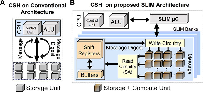
FIGURE 1. CSH performed using (A) conventional computing architecture and (B) proposed SLIM-based architecture.
In this work, we present an efficient hardware mapping of the Keccak hash function (described later) using SLIM-based methodology. The basic operations of Keccak-f algorithm are XOR/AND/NOT, which can be efficiently implemented using SLIM. As shown in Figure 1B, in the proposed SLIM-based architecture, data transfer to CPU is no longer a part of the pipeline, and only instructions are transferred between CPU and storage to complete the hashing operation. Hence, SLIM would offer enhanced security and resistance to SCA (Skorobogatov, 2017) due to negligible data movement. In the literature, LIM methodologies have been proposed for different cryptographic applications such as SHA-3 (Bhattacharjee et al., 2017; Nagarajan et al., 2019; Yang and Chen, 2019) and Advanced Encryption Standard (AES) (Angizi et al., 2018; Xie et al., 2018). Compared to the literature, following are the novel contributions of this work:
• A modified SLIM bank design (by incorporating SHIFT registers) was adapted specifically to execute CSH applications.
• New mapping methodology for realizing Keccak-f (using XOR, AND, and NOT gates) on a SLIM MAT (matrix).
• Performance analysis (energy and latency) w.r.t. conventional architectures using emerging NVM technologies such as CBRAM (conductive bridge RAM), OxRAM (oxide RAM), PCM (phase change memory), and FeRAM (ferroelectric RAM).
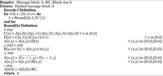
Algorithm 1 Keccak-f round algorithm.
Section 2 summarizes basics of the Keccak-f algorithm, presents the SLIM methodology and its hardware realization, and describes the proposed hardware mapping methodology with operation and instruction level details. Section 3 summarizes the key analysis results, and Section 4 provides the conclusion.
2 Materials and Methods
2.1 Basics of Keccak-f
CSH refers to security-oriented usage of hashing functions that ensure very high difficulty for inverse transformations, making them strongly unidirectional (Chi and Zhu, 2017). The primary properties associated with CSH are the following:
1. Pre-image resistance: Input data (message) is difficult to find if only output data (message digest) is known.
2. Second pre-image resistance: Given a message mi and its hash output hash(k,mi), where k is the hash key, it is difficult to find another message mj satisfying hash(k,mi) = hash(k,mj).
3. Collision resistance: Two messages mi and mj should have different hash results in order to avoid birthday attacks (Bellare and Kohno, 2003).
While the length of input data, i.e., message for CSH function is arbitrary, the output, i.e., message digest has a fixed length. Fixed-sized hashes are used to represent the original input for validation. Due to the security aspect, any small change in input requires a significant change in the output. CSH can be further divided into two categories: 1) keyed cryptographic hashing and 2) unkeyed cryptographic hashing. The current standard for unkeyed cryptographic hashing is SHA-3 also known as Keccak (Bertoni et al., 2013). A permutation block (Keccak-f) is used as the core operation. The Keccak-f is realized by multiple rounds (here 24) of 5-steps (θ, ρ, π, χ, and ι) with logic operations and bit-wise permutations. It operates on a fixed number of bits “b”, i.e., width of the permutation or bit state. In this study, we consider Keccak-f implementation with block-size “b” = 1,600. Input and output entries of Keccak-f round function are 5 × 5 matrices of 64-bit words. The complete process for hashing with steps is shown in Algorithm 1. Message block “A” and round constant “RC” are provided as inputs. Variables “x” and “y” represent the matrix index, and operations on “x” and “y” are in modulo 5 (i.e., maximum value is 4, and any further increase starts the cycle back from 0). Variables “B”, “C” and “D” are used to hold intermediate values. In ρ step, r(x, y) represents the rotation matrix, and “A” is rotated according to the “r” matrix values. Round and rotation constants are given in Dworkin, (2015). Final computed hash is stored in “A”.
2.2 SLIM: Concept and Methodology
SLIM methodology (Kingra et al., 2020) relies on exploiting multilevel capability (MLC) of emerging NVM devices to use the same memory cell for both “storage” and “logic” functions simultaneously. In SLIM, rather than storing input variables in the bitcell, the aim is to preserve the initial memory state. For that, at least four distinct resistance states are essential (states S1, S2, S3, and S4 in Figure 2B). Hence, MLC NVM devices that exhibit repeatable analog conductance tuning behavior can be utilized to realize the SLIM approach. Each of the four selected states are assigned to both logic (“1”/“0”) and memory (LRS/HRS) definitions. The sense amplifier (SA) threshold/memory state-sensing window is defined such that two states lie in the memory LRS sense region while other two in the memory HRS sense region. The two states in the memory LRS region (here S1 and S2) are assigned Logic “1” and Logic “0” values, respectively. Similarly, the memory HRS region states (here S3 and S4) are assigned Logic “1” and Logic “0” values. There are two representations for each resistance state: consider state S1, it has Logic “1” and Memory “LRS” label. While executing any logic operation, the SLIM programming scheme permits state transitions only within the Logic (“1”/“0”) levels of a particular memory sense region (i.e., Logic “1” ↔ “0” within HRS or within LRS sense regions are permitted, but Logic “1” ↔ “0” through HRS ↔ LRS is not permissible). Thus, any initially stored memory state on the bitcell can be preserved even after executing a logic operation.
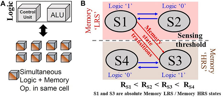
FIGURE 2. (A) Illustration of SLIM paradigm showing all memory blocks capable to perform storage and logic operations simultaneously and non-destructively. (B) SLIM state assignment along with Memory/Logic labels and permissible state transitions.
2.2.1 Device Fabrication for Experimental Validation
Analog resistive switching OxRAM stacks of the Ni/3-nm HfO2/7-nm Al-doped-TiO2 (ATO)/TiN (top to bottom) structure were fabricated by following a CMOS compatible process. The transmission electron microscopy (TEM) cross-section image of the device stack is shown in Figure 3A, where amorphous dielectric bilayer is seen deposited on the TiN bottom electrode (BE) film. The device fabrication flow is as follows: First, the 100-nm thick TiN BE film was deposited on the thermal-SiO2 (500 nm)/Si wafer by physical vapor deposition (PVD), RF magnetron sputtering. The BEs were then patterned by optical photolithography (first mask) and dry etching using inductively coupled plasma (ICP). At the bottom, 7-nm thick ATO dielectric was then deposited by interchanging varying amounts of TiO2 and Al2O3 PE-ALD (plasma-enhanced atomic layer deposition) cycles. At the top, the 3-nm thick dielectric HfO2 film was deposited using TDMAHf (tetrakis(dimethylamido)hafnium) and O2 plasma. Next, the 100-nm thick Ni TE (top electrode) film was deposited by DC sputtering and patterned using the lift-off technique. Final photolithography (third mask) and ICP dry etching step was performed to open the contact windows (etch the dielectrics) to the BE contact pads.
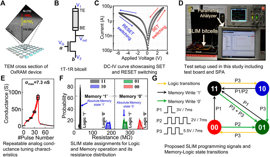
FIGURE 3. (A) OxRAM device used for this study. (B) 1T-1R SLIM bitcell. (C) DC-IV characteristics of the OxRAM device. Applied Voltage indicates VTE - VBE. TE indicates the top electrode, and BE indicates the bottom electrode. (D) Experimental test-bench used in this study. (E) Analog conductance tuning characteristics using identical SET (VSET = 3V) and RESET (VRESET = −5.5 V) pulses (includes C2C variability over 30 cycles). (F) SLIM state assignments for logic and memory operations. Histograms indicate resistance distributions for four selected SLIM states on 1T-1R SLIM bitcell (≥100 trials). (G) SLIM programming signals and memory–logic state transitions for 1T-1R SLIM bitcell.
2.2.2 Experimental Validation of SLIM
OxRAM-device (Figure 3A) based 1T-1R SLIM bitcell configuration (Figure 3B) is adopted for the proposed method (Kingra et al., 2020). The DC-IV curve of the characterized OxRAM device is shown in Figure 3C. The experimental setup (including integrated 1T-1R SLIM bitcell, CMOS chip, OxRAM chip, and parameter analyzer) used in this study is shown in Figure 3D. From the continuum of attainable OxRAM resistance levels (Figure 3E), four distinct resistance states are selected. These states are labeled as “11”, “10”, “01” and “00”. The resistance distribution for the selected states is presented in Figure 3F. As shown in Figure 3F, each of these four selected states are allotted both logic (“1”/“0”) and memory (“LRS”/“HRS”) definitions. Input variables are mapped onto the gate terminal (VG) and source terminal (V2) of the selector (NMOS transistor in this case). Before executing any logic operation, stored data on the bitcell can be either in Memory State “1” (i.e., absolute Memory state “11,” “LRS”) or Memory State “0” (i.e., absolute Memory state “01,” “HRS”). While performing a logic operation, there are chances the bitcell can make a transition from “11” → “10” or “01” → “00”. To perform consecutive logic operation on the same bitcell, the bitcell is assumed to be in absolute memory state (“11” for Memory “LRS” and “01” for Memory “HRS”); hence, the bitcell needs to be reinitialized to an absolute memory state in case state transition happens while executing logic operation. The SLIM programming signals and memory–logic state transitions for 1T-1R bitcell are shown in Figure 3G. As observed, the initially stored memory state of the bitcell is preserved even after executing a logic operation. Computation mapping is performed for realizing Keccak-f using XOR/AND/NOT gates and SHIFT registers as building blocks. SLIM bitcells are used for realizing XOR/AND/NOT gate functionalities. A single 1T-1R bitcell can realize NOT/NAND gates. XOR/AND logic is realized using 4/2 SLIM NAND logic gates. Programming signal mapping for possible 1-bit, 2-input (a, b) operand combinations are shown in Figure 4A. As discussed earlier, before executing SLIM logic, the bitcell should be in absolute Memory State “11” or “01”. Operands a/b are mapped to VG/V2 terminal of bitcell, respectively, keeping V1 grounded (V1, V2, and VG shown in Figure 3B). Voltage conditions for operand mapping are: a = “0”/“1” indicating VG = 0/VDD, respectively. b = “0”/“1” indicating V2 = 0 V/5.5 V, respectively. When both a = b = “1” (Logic high), the applied programming voltage drops across the OxRAM device, and it undergoes RESET switching, i.e., its device resistance increases and the current flowing through the device decreases. Figure 4B shows experimental results for NAND logic operation on SLIM bitcell for the initial device state: “11” (i.e., stored Memory State = LRS/“1”). Truth table for the 2-input NAND gate using a single 1T-1R SLIM bitcell is shown in Figure 4C. An example of mapping basic logic gates used in the study (NOT, AND, XOR) using SLIM is shown in Figure 5.
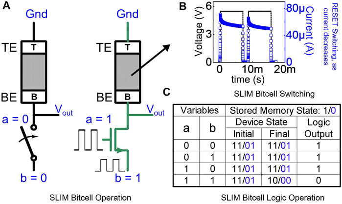
FIGURE 4. (A) Operand mapping for NAND gate logic realization in 1T-1R SLIM bitcell operation. (B) Reset switching action observed during NAND logic realization for a = b = “1,” resulting in final Logic state = “0”. (C) Truth table summarizing NAND gate operation.
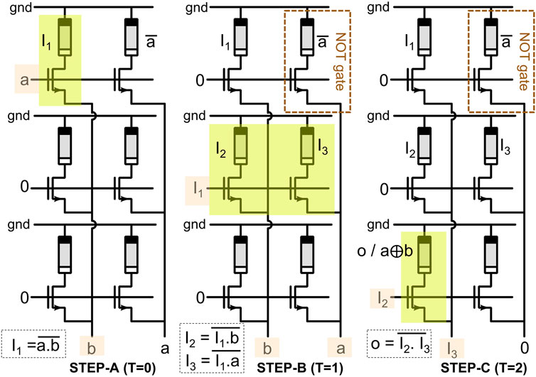
FIGURE 5. Illustration of XOR/NOT operation mapping on SLIM MAT with each SLIM bitcell performing NAND logic depending on the inputs. XOR operation takes three cycles of SLIM operations. Intermediate logic outputs are read and stored in buffer memory (see Figure 1A) for further signal application. AND operation can be realized by using NAND gate followed by a NOT gate and thus require 2 SLIM bitcells.
2.2.3 SLIM Operation Mapping
To perform computation mapping on SLIM, an estimation model is developed with the following inputs: 1) operation breakdown in terms of Intel-based instructions, 2) memory interface parameters (bandwidth and data width for cache and DRAM, etc.), 3) SLIM MAT size, and 4) MLC device parameters (energy and latency for read/write operations). Using this, a dataflow graph is realized in order to estimate possible optimization strategies for pipelining as well as performing parallel computation. Once dataflow is selected by the user, an energy and latency estimation is generated with the selected MLC device utilized in the SLIM implementation (details provided in Eqs 1, 2 ). The complete process is summarized in Figure 6.
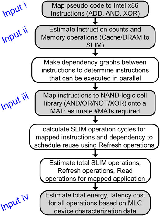
FIGURE 6. Flowchart describing steps followed for workload mapping on a SLIM MAT and energy/latency estimation. Here, pipeline stages refer to independent large functions extracted by dividing the workload into independent steps without external data dependency.
2.3 Proposed Keccak-f Mapping
Using the customized SLIM operation mapping method, CSH function SHA-3 is mapped on the SLIM MAT. First, the base Keccak-f in SHA-3 is broken down into a series of steps (refer Algorithm 1, i.e., θ, ρ, π, χ, and ι). The message is read from the main memory with block-size = 1,600 bits. Each message block (“A”) is mapped onto SLIM MATs in the form of a 5 × 5 matrix with cell size of 64-bits. Since variables/matrices “A” and “B” both need to be presented simultaneously starting from step ρ, the maximum memory required would be double the message block size (i.e., 64 × 5 × 5 × 2). Therefore, a MAT size of 64 × 64 is selected. Table 1 lists the number of logic operations (NOT, AND, SHIFT, and XOR) required at each step. Figure 5 illustrates operand mapping and XOR/NOT logic realization using SLIM methodology highlighting cycle count and SLIM bitcell requirement. Table 1 lists operation count and required SLIM MATs for each computation step in Keccak-f. Complete flow for operation mapping and energy estimation is described in Figure 6. Figure 7A illustrates data-flow mapping on the 64 × 64 SLIM MAT. We map the original data matrix “A” (5 × 5 × 64 bit words) in first 25 rows of the MAT, where entries from the same row of the matrix are arranged in neighboring rows. The row below in which matrix “A” is allocated holds the round constant RC (64-bits). Consecutive steps show data allocation in the MAT evolving during execution of the 5-steps for a single round of Keccak-f (see Table 1). An important point to note here is the ability to reuse the MAT storage for variables “B”, “C”, and “D” since intermediate data are stored as the logic state of the bitcell. For calculating matrix “C”, XOR operations are mapped on bitcells already storing matrix “A”. This minimizes additional bitcell requirement for logic computation, while preserving original data matrix “A” for further use. To reuse the selected MAT for multiple compute runs, intermediate refresh operations are carried out by programming the device to absolute memory state. In refresh scheme, first, the initial state of the bitcell is read. If the bitcell is in absolute memory state (i.e., “11”or “01”), logic operation can be performed directly. However, in case the state of bitcell is in non-absolute memory state (i.e., “10” or “00”), refresh signal is applied, and the bitcell is restored to its corresponding absolute memory state (“11” or “01”) before executing logic operation on that bitcell. To estimate energy dissipation for combinational logic operations realized using SLIM bitcells, an empirical model is built based on Eq. 1. Total energy dissipation for performing CSH computation on SLIM MAT is described in Eq. 2.
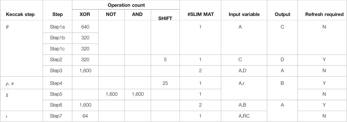
TABLE 1. Operation mapping of Keccak-f steps on SLIM MATs.
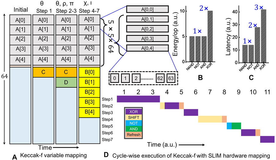
FIGURE 7. (A) Variable mapping for Keccak-f function realized on SLIM MAT of size 64 × 64. SLIM-based logic gate realization estimates of: (B) energy and (C) latency. (D) Cycle-wise mapping of operations on SLIM MAT for a single round of Keccak-f function. Each time unit represents computation time for a XOR (3 × SLIM) operation.
Here, N denotes total possible combinations of input xi. Switch_events is an empirical model to determine worst-case state transition events at each node of the NAND logic-based computation graph considering all input combinations for specified logic operation. For example, when performing an AND operation, two SLIM bitcells are used (first SLIM bitcell acting as NAND gate and the other acting as NOT gate). Depending on the input combinations/operands, one of the two SLIM bitcells will undergo switching (Logic “1” → Logic “0”). For instance, if the logic output of NAND is “1” (for input combinations: “00”, “01”, “10”), NOT gate will undergo Logic “1” → Logic “0” switching; whereas for input combinations “’11,” NAND gate undergoes Logic “1” → Logic “0” transition, and NOT gate will exhibit Logic “1” state. Refreshenergy accounts for number of refresh operations carried out over the SLIM MAT during execution of the CSH workload (Kingra et al., 2020). Readenergy accounts for reading of the output state in order to chain the operation. However, in comparison to Switchenergy and Refreshenergy, the Readenergy component of device dissipation is insignificant. Decoderenergy is estimated based on the literature (Viveka and Amrutur, 2014). Since SHIFT/rotate operation is not possible with the proposed SLIM bitcell, additional CMOS SHIFT registers are included in the SLIM bank design. The reference energy value for SHIFT registers in periphery is estimated from Woo et al., (2019) (denoted by SHIFTenergy). Nshift represents number of SHIFT operations performed for the CSH workload. To estimate latency values, the worst path from the input to output node of the NAND logic-based computation graph is used.
Energy dissipation/op and latency estimates for desired logic gates using the SLIM mapping strategy are shown in Figures 7B,C, respectively. A cycle-wise execution time-chart for the CSH workload is shown in Figure 7D. In step θ, 5-input XOR operation is split into 3 steps as SLIM bitcell realizes 2-input XOR logic gate. All bitcells in a row of the SLIM MAT can be operated in parallel. For the current study, a SLIM MAT of size 64 × 64 is selected that can perform 4096 NAND operations. Exploiting maximum possible parallelism, two streams of 2-input-independent XOR operations can be carried out in Step1a resulting in 640 XOR operations. Hence, out of 1280 XOR operations, 640 are completed in Step1a followed by 320 each in Step1b and Step1c, respectively. Similarly, the cycle count has been reported for the remaining Keccak-f steps. Each XOR operation requires three compute/write cycles and four read cycles. The overall execution of a single round of Keccak-f requires ≈24k NAND logic operation that exceeds the overall capacity of the two SLIM MATs, i.e., ≈ 8k. Hence, refresh operation is carried out three times as depicted in Figure 7D.
3 Results and Discussion
3.1 Performance Benchmarking for Proposed SLIM-Based Keccak-f
Comparison of conventional architecture with proposed SLIM-based architecture for CSH workload is shown in Table 2. Here, it is assumed that data/message are fetched from the main memory (RAM) to CPU in case of conventional architecture (Intel i5 CPU with DRAM). This results in increased data transfer that costs both in terms of energy and latency as compared to proposed SLIM implementation. Logic operations are carried out inside the CPU, and message digest is stored back in the main memory. For data transfer, 128-bit-wide bus is used for all memory interfaces. In case of SLIM-based architecture, all combinational logic operations are performed using SLIM bitcells, and the corresponding energy is estimated using an approximate model described in Eq. 1. To maximize the possible parallel SLIM operations in Step3 and Step6 (from Table 1), two SLIM MATs are used, each of size 64 × 64 (i.e., 512 B). This results in maximum number of parallel 8,192 (2 × 64 × 64) SLIM operations. SLIM-based architecture is realized using four different emerging NVM device technologies (Choi et al., 2020), i.e., CBRAM, OxRAM, PCM, and FeRAM. By performing all computations inside the SLIM MAT, the total EDP (energy delay product) for the CSH workload reduces by 300× in case of FeRAM-based SLIM. Total EDP for SLIM-based implementations can be broken down into four operation types (i.e., data transfer, SLIM-logic, Shift, and SLIM-refresh) as illustrated in Figure 8. Shift operation contribution remains constant across technologies. Data transfer relies on read operation performance of each device technology. Device programming energy/switching energy determines the cost of SLIM operations (Logic, Refresh). In case of FeRAM-based SLIM, it can be observed that dissipation due to data transfer and shift operations is higher than the SLIM operations leading to better EDP savings. However, for PCM, SLIM operations show a significant energy contribution due to higher switching energy of the PCM device from the literature (see Table 2), thus leading to higher EDP. A significant advantage of the proposed hardware mapping scheme is the possibility to exploit parallelism based on high density of NVM devices. Considering a 1-Gb SLIM memory bank with MAT size 64 × 64, it would be possible to perform 128k Keccak-f round functions in parallel over different blocks of a large message, i.e., 200-Mb data can be processed in parallel. In case of CPU-based approaches, the maximum parallelism is limited to total number of cores available, i.e., 32 for typical modern-day computers.

TABLE 2. Performance benchmarking of SLIM-based Keccak-f for a single round using various device technologies from the literature.
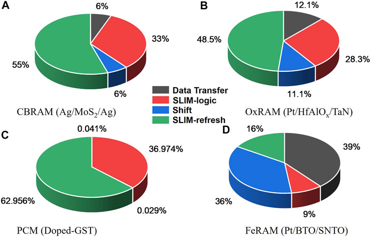
FIGURE 8. Energy contribution breakdown based on operation type when mapping Keccak-f computation on SLIM bitcells using device stacks: (A) CBRAM (Ag/MoS2/Ag), (B) OxRAM (Pt/HfAlOx/TaN), (C) PCM (doped-GST), and (D) FeRAM (Pt/BTO/SNTO).
3.2 SLIM Implementation and NVM Device Reliability
The reliability of SLIM bitcell is primarily dependent on device endurance, programming variability, and the conductance values for selected SLIM states. SLIM bitcell operation relies on device state switching while performing a logic operation and hence faces a fundamental limitation due to limited endurance of NVM devices. As shown in Table 2, NVM device endurance is typically observed in the range of 104 cycles. One way to address this would be to map the application over a larger SLIM bitcell array, thus reducing requirement of switching-events required per device at the cost of additional latency due to data movement. However, through design optimizations, improved device endurance

TABLE 3. NVM device technology comparison in terms of reliability parameters.
3.3 Comparison With Other LIM Methods
SHA-3 computation using NVM-based LIM has been proposed in recent works (Bhattacharjee et al., 2017; Nagarajan et al., 2019; Yang and Chen, 2019). Table 4 compares the current implementation with respect to recent studies in terms of the LIM-operating principle. As shown in Table 4, the SLIM methodology helps in realizing the universal NAND logic gate using any two terminal NVM devices exhibiting MLC. This enables realization of complex logic operations by breaking it down into series of NAND gates. In this study, architecture exploration has been confined to 2-input XOR logic gates for CSH workload; however, SLIM offers flexibility to map n-input XOR logic by chaining universal 1T-1R SLIM NAND logic gates. Another advantage of SLIM over other NVM-based LIM realizations is the reduction in area overhead, since SLIM bitcells can be used simultaneously for storage as well as to map logic gates (such as XOR/AND/NOT). Performance comparison (in terms of energy dissipation/operation cycles) with prior works is not shown, since they rely on using theoretically estimated NVM device parameters in comparison to the current work that uses experimentally measured device parameters.
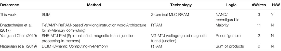
TABLE 4. Comparison of proposed SLIM-based SHA-3 implementation with other works in the literature based on NVM-based LIM.
4 Conclusion
In this work, we present step-by-step implementation of Keccak-f function using NVM-based SLIM methodology. Experimental validation of SLIM methodology using bilayer OxRAM devices is performed. A new mapping strategy was proposed, and simulation-based estimation of EDP was performed using state-of-the-art emerging NVM devices. A detailed discussion of trade-offs between device technologies in terms of operation reliability is also presented. Based on the analysis, FeRAM demonstrates the best performance (EDP savings of ∼ 300×) and reliability emerging as a promising candidate. Next, we also presented a comparison of the proposed method with other LIM techniques for the same application. The proposed method demonstrates improved generalization capability to optimize logic mapping (universal gate) and better area savings (co-location of logic and memory) while minimizing write operations required per 1-bit XOR computation. Beyond EDP and endurance improvement, the proposed method also enhances security for hash computations due to reduced data movement by taking advantage of co-location of logic and memory. This further results in better immunity to security exploits such as SCA.
Data Availability Statement
The original contributions presented in the study are included in the article/Supplementary Material, further inquiries can be directed to the corresponding author.
Author Contributions
SK and VP performed experimental characterization and simulations. MS planned and supervised the project. All authors participated in data analysis and writing of the manuscript.
Funding
This work was supported in part by the DST SERB under CORE Research grant (CRG/2018/001901), in part by PSA-Prn. SA/Nanoelectronics/2017, and in part by the Department of Science and Technology—DST/TDT/AMT/2017/159(C).
Conflict of Interest
The authors declare that the research was conducted in the absence of any commercial or financial relationships that could be construed as a potential conflict of interest.
Publisher’s Note
All claims expressed in this article are solely those of the authors and do not necessarily represent those of their affiliated organizations, or those of the publisher, the editors, and the reviewers. Any product that may be evaluated in this article, or claim that may be made by its manufacturer, is not guaranteed or endorsed by the publisher.
Acknowledgments
The authors would like to acknowledge Prof. Tuo-Hung Hou for providing fabricated RRAM chips used for experimental validation in this study.
References
Angizi, S., He, Z., Bagherzadeh, N., and Fan, D. (2018). Design and Evaluation of a Spintronic In-Memory Processing Platform for Nonvolatile Data Encryption. IEEE Trans. Comput.-Aided Des. Integr. Circuits Syst. 37, 1788–1801. doi:10.1109/tcad.2017.2774291
Bellare, M., and Kohno, T. (2003). Hash Function Balance and its Impact on Birthday Attacks. IACR Cryptol. Eprint Arch. 65.
Bertoni, G., Daemen, J., Peeters, M., and Van Assche, G. (2013). “Keccak,” in Advances in Cryptology - EUROCRYPT 2013 (Springer Berlin Heidelberg), 313–314. doi:10.1007/978-3-642-38348-9_19
Bhattacharjee, D., Pudi, V., and Chattopadhyay, A. (2017). “SHA-3 Implementation Using ReRAM Based In-Memory Computing Architecture,” in 2017 18th International Symposium on Quality Electronic Design (ISQED) (IEEE), 325–330. doi:10.1109/isqed.2017.7918336
Boybat, I., Le Gallo, M., Nandakumar, S. R., Moraitis, T., Parnell, T., Tuma, T., et al. (2018). Neuromorphic Computing with Multi-Memristive Synapses. Nat. Commun. 9. doi:10.1038/s41467-018-04933-y
Chakrabarti, B., Galatage, R. V., and Vogel, E. M. (2013). Multilevel Switching in Forming-free Resistive Memory Devices with Atomic Layer Deposited ${\rm HfTiO}_{x}$ Nanolaminate. IEEE Electron. Device Lett. 34, 867–869. doi:10.1109/LED.2013.2262917
Chen, C. Y., Goux, L., Fantini, A., Degraeve, R., Redolfi, A., Groeseneken, G., et al. (2016). Stack Optimization of Oxide-Based RRAM for Fast Write Speed lessbin (1 μs) at Low Operating Current (10 μa). Solid-State Elect. 125, 198–203. doi:10.1016/j.sse.2016.05.008
Chen, Y. Y., Roelofs, R., Redolfi, A., Degraeve, R., Crotti, D., Fantini, A., et al. (2014). “Tailoring Switching and Endurance/Retention Reliability Characteristics of HfO2/Hf RRAM with Ti, Al, Si Dopants,” in 2014 Symposium on VLSI Technology (VLSI-Technology): Digest of Technical Papers, 1–2. doi:10.1109/VLSIT.2014.6894403
Choi, S. H., Park, S.-O., Seo, S., and Choi, S. (2022). Reliable Multilevel Memristive Neuromorphic Devices Based on Amorphous Matrix via Quasi-1d Filament Confinement and Buffer Layer. Sci. Adv. 8. doi:10.1126/sciadv.abj7866
Choi, S., Yang, J., and Wang, G. (2020). Emerging Memristive Artificial Synapses and Neurons for Energy‐Efficient Neuromorphic Computing. Adv. Mater. 32, 2004659. doi:10.1002/adma.202004659
Debnath, S., Chattopadhyay, A., and Dutta, S. (2017). “Brief Review on Journey of Secured Hash Algorithms,” in 2017 4th International Conference on Opto-Electronics and Applied Optics (Optronix), 1–5. doi:10.1109/OPTRONIX.2017.8349971
Dworkin, M. J. (2015). “SHA-3 Standard: Permutation-Based Hash and Extendable-Output Functions,” in Tech. rep., National Institute of Standards and Technology. doi:10.6028/nist.fips.202
Fantini, A., Goux, L., Redolfi, A., Degraeve, R., Kar, G., Chen, Y. Y., et al. (2014). “Lateral and Vertical Scaling Impact on Statistical Performances and Reliability of 10nm Tin/hf(al)o/hf/tin Rram Devices,” in 2014 Symposium on VLSI Technology (VLSI-Technology): Digest of Technical Papers, 1–2. doi:10.1109/VLSIT.2014.6894433
Feng, X., Li, Y., Wang, L., Chen, S., Yu, Z. G., Tan, W. C., et al. (2019). A Fully Printed Flexible MoS 2 Memristive Artificial Synapse with Femtojoule Switching Energy. Adv. Electron. Mater. 5, 1900740. doi:10.1002/aelm.201900740
Gao, S., Zeng, F., Wang, M., Wang, G., Song, C., and Pan, F. (2015). Implementation of Complete Boolean Logic Functions in Single Complementary Resistive Switch. Sci. Rep. 5, 15467. doi:10.1038/srep15467
Goux, L., Fantini, A., Degraeve, R., Raghavan, N., Nigon, R., Strangio, S., et al. (2013). “Understanding of the Intrinsic Characteristics and Memory Trade-Offs of Sub-μa Filamentary Rram Operation,” in 2013 Symposium on VLSI Technology, T162–T163.
Goux, L., Fantini, A., Redolfi, A., Chen, C. Y., Shi, F. F., Degraeve, R., et al. (2014). “Role of the Ta Scavenger Electrode in the Excellent Switching Control and Reliability of a Scalable Low-Current Operated TiN\Ta2O5\Ta RRAM Device,” in 2014 Symposium on VLSI Technology (VLSI-Technology): Digest of Technical Papers, 1–2. doi:10.1109/VLSIT.2014.6894401
Hudec, B., Wang, I.-T., Lai, W.-L., Chang, C.-C., Jančovič, P., Fröhlich, K., et al. (2016). Interface Engineered HfO2-Based 3d Vertical ReRAM. J. Phys. D: Appl. Phys. 49, 215102. doi:10.1088/0022-3727/49/21/215102
Joshi, V., Le Gallo, M., Haefeli, S., Boybat, I., Nandakumar, S. R., Piveteau, C., et al. (2020). Accurate Deep Neural Network Inference Using Computational Phase-Change Memory. Nat. Commun. 11. doi:10.1038/s41467-020-16108-9
Khalil-Hani, M., Nambiar, V. P., and Marsono, M. N. (2010). “Hardware Acceleration of Openssl Cryptographic Functions for High-Performance Internet Security,” in 2010 International Conference on Intelligent Systems, Modelling and Simulation, 374–379. doi:10.1109/ISMS.2010.89
Kim, I. S., Cho, S. L., Im, D. H., Cho, E. H., Kim, D. H., Oh, G. H., et al. (2010). “High Performance PRAM Cell Scalable to Sub-20nm Technology with below 4f2 Cell Size, Extendable to DRAM Applications,” in 2010 Symposium on VLSI Technology (IEEE), 203–204. doi:10.1109/vlsit.2010.5556228
Kim, K. M., Xu, N., Shao, X., Yoon, K. J., Kim, H. J., Williams, R. S., et al. (2019). Single-cell Stateful Logic Using a Dual-Bit Memristor. Phys. Status Solidi RRL 13, 1800629. doi:10.1002/pssr.201800629
Kingra, S. K., Parmar, V., Chang, C.-C., Hudec, B., Hou, T.-H., and Suri, M. (2020). SLIM: Simultaneous Logic-In-Memory Computing Exploiting Bilayer Analog OxRAM Devices. Sci. Rep. 10. doi:10.1038/s41598-020-59121-0
Kishore, N., and Raina, P. (2019). Parallel Cryptographic Hashing: Developments in the Last 25 Years. Cryptologia 43, 504–535. doi:10.1080/01611194.2019.1609130
Kwon, D.-H., Kim, K. M., Jang, J. H., Jeon, J. M., Lee, M. H., Kim, G. H., et al. (2010). Atomic Structure of Conducting Nanofilaments in TiO2 Resistive Switching Memory. Nat. Nanotech 5, 148–153. doi:10.1038/nnano.2009.456
Lee, M.-J., Lee, C. B., Lee, D., Lee, S. R., Chang, M., Hur, J. H., et al. (2011). A Fast, High-Endurance and Scalable Non-volatile Memory Device Made from Asymmetric Ta2O5−x/TaO2−x Bilayer Structures. Nat. Mater 10, 625–630. doi:10.1038/nmat3070
Li, C., Hu, M., Li, Y., Jiang, H., Ge, N., Montgomery, E., et al. (2017). Analogue Signal and Image Processing with Large Memristor Crossbars. Nat. Electron. 1, 52–59. doi:10.1038/s41928-017-0002-z
Li, J., Ge, C., Du, J., Wang, C., Yang, G., and Jin, K. (2019). Reproducible Ultrathin Ferroelectric Domain Switching for High‐Performance Neuromorphic Computing. Adv. Mater. 32, 1905764. doi:10.1002/adma.201905764
Linn, E., Rosezin, R., Tappertzhofen, S., Böttger, U., and Waser, R. (2012). Beyond von Neumann-logic operations in passive crossbar arrays alongside memory operations. Nanotechnology 23, 305205. doi:10.1088/0957-4484/23/30/305205
Luo, Y.-C., Hur, J., and Yu, S. (2021). Ferroelectric Tunnel junction Based Crossbar Array Design for Neuro-Inspired Computing. IEEE Trans. Nanotechnology 20, 243–247. doi:10.1109/TNANO.2021.3066319
Michail, H. E., Athanasiou, G. S., Kelefouras, V., Theodoridis, G., and Goutis, C. E. (2012). On the Exploitation of a High-Throughput Sha-256 Fpga Design for Hmac. ACM Trans. Reconfigurable Technol. Syst. 5, 1–28. doi:10.1145/2133352.2133354
Nagarajan, K., Ensan, S. S., Nasim Imtiaz Khan, M., Ghosh, S., and Chattopadhyay, A. (2019). “SHINE: A Novel SHA-3 Implementation Using ReRAM-Based In-Memory Computing,” in 2019 IEEE/ACM International Symposium on Low Power Electronics and Design (ISLPED) (IEEE), 1–6. doi:10.1109/islped.2019.8824979
Skorobogatov, S. (2017). “How Microprobing Can Attack Encrypted Memory,” in 2017 Euromicro Conference on Digital System Design (DSD), 244–251. doi:10.1109/DSD.2017.69
Song, T., Tan, H., Estandía, S., Gàzquez, J., Gich, M., Dix, N., et al. (2022). Improved Polarization and Endurance in Ferroelectric hf0.5zr0.5o2 Films on SrTiO3(110). Nanoscale. doi:10.1039/d1nr06983g
Sun, Z., Ambrosi, E., Bricalli, A., and Ielmini, D. (2018). Logic Computing with Stateful Neural Networks of Resistive Switches. Adv. Mater. 30, 1802554. doi:10.1002/adma.201802554
Viveka, K. R., and Amrutur, B. (2014). “Energy Efficient Memory Decoder Design for Ultra-low Voltage Systems,” in 2014 27th International Conference on VLSI Design and 2014 13th International Conference on Embedded Systems, 145–149. doi:10.1109/VLSID.2014.32
Wang, T.-Y., Meng, J.-L., Rao, M.-Y., He, Z.-Y., Chen, L., Zhu, H., et al. (2020). Three-dimensional Nanoscale Flexible Memristor Networks with Ultralow Power for Information Transmission and Processing Application. Nano Lett. 20, 4111–4120. doi:10.1021/acs.nanolett.9b05271
Wang, Z.-R., Su, Y.-T., Li, Y., Zhou, Y.-X., Chu, T.-J., Chang, K.-C., et al. (2017). Functionally Complete Boolean Logic in 1t1r Resistive Random Access Memory. IEEE Electron. Device Lett. 38, 179–182. doi:10.1109/led.2016.2645946
Woo, K.-C., Kang, H.-J., and Yang, B.-D. (2019). Area-efficient Bidirectional Shift-Register Using Bidirectional Pulsed-Latches. IEEE Trans. Circuits Syst.66, 1386–1390. doi:10.1109/tcsii.2018.2882810
Xie, M., Li, S., Glova, A. O., Hu, J., and Xie, Y. (2018). Securing Emerging Nonvolatile Main Memory with Fast and Energy-Efficient AES In-Memory Implementation. IEEE Trans. VLSI Syst. 26, 2443–2455. doi:10.1109/tvlsi.2018.2865133
Yang, C., and Chen, Z. (2019). “A Processing-In-Memory Implementation of SHA-3 Using a Voltage-Gated Spin Hall-Effect Driven MTJ-Based Crossbar,” in Proceedings of the 2019 on Great Lakes Symposium on VLSI (New York, NY, United States: ACM), 195–200. doi:10.1145/3299874.3317972
Yang, J. J., Pickett, M. D., Li, X., Ohlberg, D. A. A., Stewart, D. R., and Williams, R. S. (2008). Memristive Switching Mechanism for Metal/oxide/metal Nanodevices. Nat. Nanotech 3, 429–433. doi:10.1038/nnano.2008.160
You, T., Shuai, Y., Luo, W., Du, N., Bürger, D., Skorupa, I., et al. (2014). Exploiting Memristive BiFeO3Bilayer Structures for Compact Sequential Logics. Adv. Funct. Mater. 24, 3357–3365. doi:10.1002/adfm.201303365
Yu, S., Wu, Y., Chai, Y., Provine, J., and Wong, H.-S. P. (2011). “Characterization of Switching Parameters and Multilevel Capability in HfOx/AlOx Bi-layer RRAM Devices,” in Proceedings of 2011 International Symposium on VLSI Technology, Systems and Applications, 1–2. doi:10.1109/VTSA.2011.5872251
Zhou, Y.-X., Li, Y., Su, Y.-T., Wang, Z.-R., Shih, L.-Y., Chang, T.-C., et al. (2017). Nonvolatile Reconfigurable Sequential Logic in a HfO2 Resistive Random Access Memory Array. Nanoscale 9, 6649–6657. doi:10.1039/c7nr00934h
Zohner, M., Kasper, M., Stöttinger, M., and Huss, S. A. (2012). “Side Channel Analysis of the SHA-3 Finalists,” in 2012 Design, Automation & Test in Europe Conference & Exhibition, DATE 2012, Dresden, Germany, March 12-16, 2012. Editors W. Rosenstiel, and L. Thiele (IEEE), 1012–1017. doi:10.1109/DATE.2012.6176644
Keywords: SLIM, cyber-security, non-volatile memory, in-memory computing, hash functions, SHA
Citation: Kingra SK, Parmar V and Suri M (2022) In-Memory Computation Based Mapping of Keccak-f Hash Function. Front. Nanotechnol. 4:841756. doi: 10.3389/fnano.2022.841756
Received: 22 December 2021; Accepted: 07 February 2022;
Published: 16 March 2022.
Edited by:
Rohit Abraham John, ETH Zürich, SwitzerlandReviewed by:
Omid Kavehei, The University of Sydney, AustraliaYoeri Van De Burgt, Eindhoven University of Technology, Netherlands
Copyright © 2022 Kingra, Parmar and Suri. This is an open-access article distributed under the terms of the Creative Commons Attribution License (CC BY). The use, distribution or reproduction in other forums is permitted, provided the original author(s) and the copyright owner(s) are credited and that the original publication in this journal is cited, in accordance with accepted academic practice. No use, distribution or reproduction is permitted which does not comply with these terms.
*Correspondence: Manan Suri, bWFuYW5zdXJpQGVlLmlpdGQuYWMuaW4=
†These authors have contributed equally to this work