 Amardeep Bharti
 Alessio Turchet
 Benedetta Marmiroli
- 1Elettra-Sincrotrone Trieste, Trieste, Italy
- 2Institute of Inorganic Chemistry, Graz University of Technology, Graz, Austria
X-ray lithography has been first proposed almost 50 years ago, and the related LIGA process around 25 years ago. It is therefore a good time to make an analysis of the technique, with its pros and cons. In this perspective article, we describe X-ray lithography’s latest advancements. First, we report the improvement in the fabrication of the high aspect ratio and high-resolution micro/nanostructures. Then, we present the radiation-assisted synthesis and processing of novel materials for the next generation of functional devices. We finally draw our conclusion on the future prospects of the technique.
Introduction
In the X-ray lithography (XRL) process, some materials, called resists, which are sensitive to X-rays and change their dissolution rate in a specific solvent after irradiation, are exposed to an X-ray source through a mask and can be patterned. The mask is composed of heavy Z-elements (Au, W, etc.) acting as absorbing region, while the carrier substrate is composed of low-attenuation elements (Si, Be, diamond, SiC, SiNx, etc.) (Tormen et al., 2011). The idea of the XRL was first proposed by H. Smith and Spears in 1972 (Spears and Smith, 1972; Smith et al., 1973) and attained the attention of the micro/nanofabrication community due to its shorter wavelength and larger penetration depth than conventional UV lithography, offering new possibilities to build micro-devices with high aspect ratio, thick resists, and almost vertical sidewalls (Maldonado et al., 1975; Maydan et al., 1975). XRL is the basic step of the LIGA process [German acronym of Lithographie Galvanoformung Abformung meaning lithography electrodeposition, molding (Becker et al., 1986)] that includes the electrodeposition of metal in the developed resist structure in order to obtain a mould or an electrode for a subsequent replication process like molding or electro discharge machining. X-rays can be distinguished as soft, with an energy range from 150 eV to ∼2 keV, and hard (or deep) with energy >5 keV. Soft XRL is suitable for high-resolution structures (<50 nm) with limited resist thickness. Deep XRL (DXRL) is commonly used for the LIGA process and to irradiate thick resists (hundreds of microns). At present, the XRL technique is available at synchrotron radiation facilities.
The semiconductor industry interest in XRL is related to the definition of technological nodes. The term refers to a specific semiconductor manufacturing process and to its design rules: initially, the node number defined the gate length or half-pitch (HP), whereas at present (below 22 nm) it relates to a specific generation of chips fabricated with a particular technology. Due to the shorter wavelength with respect to UV, XRL potentially ensures a “resolution reserve” for all the technological nodes. Moreover, it does not require a different facility at each technological node like UV lithography. However, the potentiality of the technique was not fully exploited, as efforts focused first on UV then on EUV lithography (Tormen et al., 2011). More recently, XRL has attracted new attention for the Next 2 node (beyond the 10-nm technological node) onward, mainly due to the potentiality of soft X-ray interference lithography (Wu et al., 2020, Mojarad et al., 2015c).
Maldonado et al. have recently given an overview of XRL and its potentiality (Maldonado and Peckerar, 2016), which is an essential read to understand the technology. With this background, in our communication we will present the limits of the technique and its recent advances both in the micro/nanofabrication of devices and in the radiation-assisted synthesis and processing of materials, showing why we believe that there can still be a future for such a unique technology.
Fabrication of micro/nanostructures
Upgrades of the standard XRL technique
After the appearance of the first generation of commercially available X-ray scanners in the late 90s, several upgrade projects were independently developed in the synchrotron radiation facilities. Improvements mainly concerned three axis stages to move the sample holder, two rotational axes to allow tilted exposures, moving mask stages (Goldenberg et al., 2016), and alignment systems for multiple exposures with different masks. These technical advances opened new routes as described in the following.
Dynamic XRL
It is a method where the mask and the sample holder can be driven independently, allowing to perform a gray-scale dose distribution exposure (Pindyurin et al., 2008). With the beam scan method, shown in Figure 1A, the sample stage is moved alternately in vertical and horizontal directions, and large areas can be exposed even if the beam size is small (Takeuchi et al., 2019).
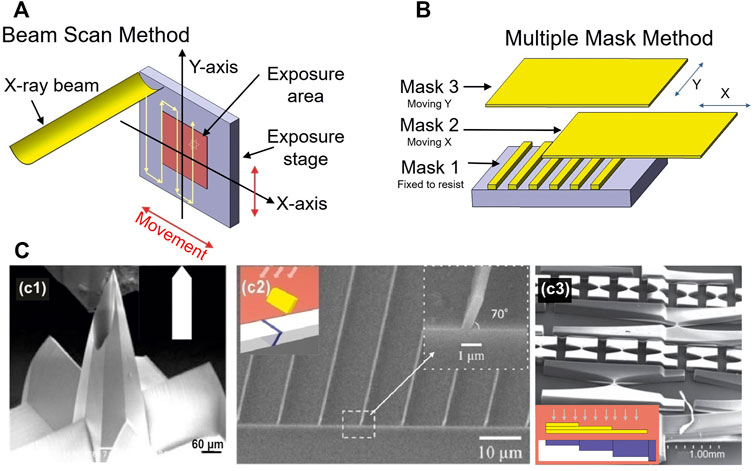
FIGURE 1. (A) Scheme of the beam scan method. The exposure stage (assembly of mask and sample) is moved with respect to the beam during exposure. (B) Scheme of the multiple mask lithography, where superimposed masks are moved while irradiating. The idea comes from Moser et al. (2012). (C) Examples of 3D structures obtained with XRL. (c1) 3D Microneedle fabricated using three aligned exposures of which two are dynamic by moving an obelisk-shaped absorber mask (shown in the inset) first in one direction, and then at 90° on the same plane. In this way, the pyramid needle is obtained. A third static exposure is performed to obtain the needle hole. Adapted from Wang et al. (2021) (c2) Oblique submicron structures of a 10-μm period at 20° obtained with a slanted mask and exposure (shown in the inset). Adapted from Kim et al. (2021). (c3) Step-like microstructures with height 250 and 150 µm obtained by changing the absorber thickness of the mask. Adapted from Nazmov et al. (2020) with permission of AIP Publishing.
Multiple mask lithography
The system, schematized in Figure 1B, is based on the use of several superimposed masks whose position can be controlled over time during the exposure phase, creating a gray-scale dose distribution over a specific area (Moser et al., 2012).
Pencil-beam mode exposure
Is based on a pre-collimator which limits the irradiation field, while the motion of the sample holder during the exposure allows to “draw” on the resist layer. Furthermore, using a mask, the beam is divided into several microbeams reducing the exposure time for array structures (Goldenberg et al., 2016).
With such systems, it is possible to go beyond the typical 2.5D extruded structures and obtain 3D ones as demonstrated by several recently published research works. Just to name few, Moser et al. (Moser et al., 2012) used multiple-mask lithography to fabricate a 3D micromirror. Wang et al. (Wang et al., 2021) fabricated a 3D array of obelisk-shaped microneedles by three aligned exposures of which two were conducted moving the resist in front of the mask during irradiation. The final structure is shown in Figure 1c1. Kim et al. (Kim et al., 2021) controlled the oblique angle of submicron-scale structures over centimeter-scale areas using an inclined X-ray exposure through a mask with slanted structures. They produced high-aspect-ratio patterns angled at 20° and 10°, respectively, shown in Figure 1c2. Nazmov et al. (Nazmov et al., 2020) obtained combined elements by using a stepped attenuator of the X-ray beam and by changing the absorber thickness of the mask. They fabricated refractive X-ray lenses with a parabolic cylinder profile and different height, shown in Figure 1c3. Zhang et al. (Zhang et al., 2021) proposed a method based on the exposure of the resist on a flexible substrate, fabricating spherically curved microstructures as micro-slot optics for astronomical telescopes.
Maskless XRL
Leontowich et al. (Leontowich et al., 2013) used an SR scanning transmission X-ray microscope (STXM) equipped with a double-Fresnel zone plate lens to direct write 15-nm-wide features in PMMA resist. Späth et al. (Späth et al., 2016; Späth et al., 2019) employed STXM to obtain metallic nanostructures from metal organic precursor gases.
X-ray Interference Lithography
Numerous factors limit the resolution in XRL. Among the others, we cite beam divergence, Fresnel diffraction, generation of photoelectrons in the resist, and thermal deformation of the mask (Tormen et al., 2011). Some of them have been addressed. For example, both diffraction and penumbral blur depend on the gap between the mask and the resist, and its minimization by making hard contact was investigated by Saegusa et al. (Saegusa, et al., 2021).
The diffraction issue, which was considered a major drawback, is now being exploited in the X-ray interference lithography (XIL) (Mojarad et al., 2015a). In XIL, the incident beam is transmitted and diffracted by mask gratings at certain angles, θd, given as:
where n is the order of diffraction and Pg is the grating periodicity. For instance, if two gratings are exposed to the same beam intensity, the diffracted beam would interfere with the periodicity P of the aerial image as the following:
θ is the angle between two beams = 2θd, thus P = Pg/2n. In case of the first-order diffraction-based XIL, a half-pitch HP = Pg/4 could be achieved, showing how promising is XIL for nanopatterning.
Soft X-rays are used (140–500 eV) as they provide a good trade-off between the diffraction-limited resolution and photoelectron-blur/penumbral limited resolution (Reznikova et al., 2008). Deng et al. (Deng et al., 2021) fabricated a nanoscale reference grating having a nonlinear deviation below ±0.5 nm and a maximum variation in calibrated mean pitch 0.01 nm using a combination of laser-focused atomic deposition and XIL. Mojarad et al. (Mojarad et al., 2021) obtained nanopillars with a high aspect ratio and variable opening diameter (40–100 nm) as a function of exposure dose, using 4-beam XIL and electroplating, as shown in Figure 2A. They also achieved pillars and beam structures at oblique angles of 30° and 20° using 4-beam and achromatic-Talbot geometry, as shown in Figure 2B. The shape, periodicity, and relative arrangement of the structure could be tailored using different geometrical arranged gratings. Zhao et al. (Zhao et al., 2020) demonstrated the possibility to obtain large areas of high-resolution and aspect ratio periodic nanostructures.
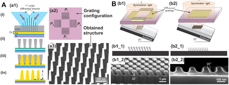
FIGURE 2. (A) Scheme of the XIL technique (a1) basic principle 1) soft X-ray irradiation of HSQ resist on a silicon substrate with base plating. Only two of the four interfering beams are shown, 2) nanostructures in HSQ resist after development, 3) Cr etching and Au electroplating using HSQ as a template and, 4) final structures in Au after removing the resist (a2) four-grating configuration for coherent (P1 = P2) and incoherent (P1≈P2) interference. (a3) Scanning-electron micrographs (45° tilt) of Au nanopillars with an aspect ratio of ∼6. (B) Exposure scheme (b1, b1_1, b2, b2_1) and resulting oblique structures (b1_2) at 30° and (b2_2) 20°. Adapted from Mojarad et al. (2021) with permission of AIP Publishing.
XIL is a promising tool for future nanofabrication; however, it still requires intense research both in photoresists and in instrumentation. The performance of the XIL in terms of RLS (resolution, linewidth roughness, and sensitivity) has been examined on different photoresists (CAR-organic chemically amplified resist, hydrogen silsesquioxan (HSQ)-inorganic hydrogen silsesquioxane, Inpria XE15IB (IB)-hafnium-based inorganic photoresist). It was observed that the patterning down to HP = 22 nm is possible for all resists, whereas in the case of Inpria HP it can reach 18 nm (Mojarad et al., 2015b, 2013). Shot-noise effect, due to the statistical fluctuation of the illumination intensity at the pattern edge, influences the solubility of the resist (Kruit and Steenbrink, 2005). It is the limiting factor that hinders the resolution, and it could be overcome by the proper choice of a photoresist. In this regard, organic photoresists do not satisfy the RLS requirements, while inorganic resists, having high absorption in XRL, would be promising candidates to surpass the existing barriers and reach the future technological nodes (Mojarad et al., 2015b).
Industrial applications
The high costs inherent to the construction and operation of synchrotron radiation facilities and the XRL process low throughput have limited its industrial applications. However, there are some specific applications for which XRL is the most suitable and effective technique.
Spectrometers
Currently, XRL’s most important industrial exploitation concerns the fabrication of diffractive and refractive optics used in X-ray microscopy, interferometry, and tomography. A historically successful application is the spectrometer, used for sensing in the UV-VIS range, for biological and clinical systems, calorimeters, food inspection, and fluorescence measuring devices (Müller and Mohr, 1993; Crocombe, 2008). The presently commercially available spectrometers use Echellette diffraction gratings in the Rowland configuration fabricated by the LIGA process. Their optical surfaces present sub-micrometric features while the optics overall dimensions are of the centimeters order.
Gratings
A further application is the X-ray grating interferometry used for medical imaging, tomography, biology, and material inspection. The latest developments in the field are the X-ray dark-field imaging system, which uses three different gratings (Pfeiffer et al., 2009; Notohamiprodjo et al., 2020), and the phase-contrast imaging with a far-field interferometer. In the latter instrument, 200-nm period multilayer gratings are used, manufactured by LIGA (Wen et al., 2013).
Radiation-assisted synthesis and processing of novel materials
Since the beginning of XRL, attention has been drawn on the effect of irradiation on different materials, beyond the ones designed and employed as standard resists. Both soft and hard X-rays can be employed, depending on the X-ray absorption coefficient and sensitivity of the materials. Recently, with the progress of material science and the production of novel functional materials with tailored properties, the possibility of their patterning and positioning has given a new boost to XRL. In fact, a new generation of microdevices like (bio) lab-on-chip, (bio) sensors, energy harvesting, and solar cells, can be envisioned.
X-ray exposure can induce simultaneous synthesis and processing of materials. The following areas have been investigated.
Sol-gels
Liu et al. (Liu et al., 2003) patterned sol–gel thick spin-on-glass films via XRL. Some years later, Brusatin et al. developed hybrid sol–gel films and hybrid organic inorganic materials as resists with tunable properties (i.e., refractive index or light absorption) (Brusatin et al., 2008; Brigo et al., 2011; Zanchetta et al., 2013; Brigo et al., 2014; Garoli et al., 2016). Falcaro et al. were the first to pattern mesoporous films from sol–gels, obtaining micropatterns of mesopores (Falcaro et al., 2008; Falcaro et al., 2009a; Falcaro et al., 2009b). Faustini et al. exposed more complex mesoporous structures (Faustini et al., 2010). The effect of irradiation on sol–gel films is well described by Innocenzi et al. (Innocenzi et al., 2011, Innocenzi et al., 2014). Research on mesoporous materials is moving forward to practical applications. The mechanical properties of irradiated mesoporous silica films were investigated (Steinberg et al., 2021) together with their application as sensors (Doherty et al., 2012) or as active sample holders able to deliver fluids (Marmiroli et al., 2021). Recently, silica–titania thin films were exposed using X-ray laboratory sources (Royon et al., 2020), opening their use to a wider community not strictly related to synchrotron radiation.
Nanoparticle Formation
Zanoni et al. (Zanoni et al., 1989) employed SR to dissociate Mo(CO)6 and produce a metallic overlayer. Eichelbaumm et al. (Eichelbaum et al., 2008b; Eichelbaum et al., 2008a) irradiated gold and silver-doped soda lime silicate glasses obtaining gold dimer particles embedded in the glassy matrix. Bertino et al. (Bertino et al., 2007) used X-rays to photodissociate a chalcogenide precursor inserted in a silica hydrogel and got metal nanoparticles as semiconductor quantum dots. Malfatti et al. added a metal precursor to the sol–gel and exposed both to X-rays, obtaining gold (Malfatti et al., 2010) and silver nanoparticles (Malfatti et al., 2011, 2016) in a patterned mesoporous matrix. Pinna et al. synthesized cerium oxide inside mesoporous films (Pinna et al., 2013).
Metal Organic Frameworks (MOFs)
A low X-ray irradiation dose does not affect the structure of ZIF (zeolitic imidazolate framework)-based MOFs, as evidenced by the research of Dimitrakakis et al. (Dimitrakakis et al., 2012). More recently, the effect of X-rays on ZIFs was explored by Widmer et al. (Widmer et al., 2019), where high doses led to the structure amorphization. DXRL was used to directly pattern ZIFs by Tu et al. (Tu et al., 2020), opening the possibility to fabricate microdevices and sensors composed of tailored MOFs.
Others
Heya et al. (Heya et al., 2020, Heya et al., 2021) irradiated pentacene to obtain nanographene. Evlyukhin et al. (Evlyukhin et al., 2018) reported the combination of high-pressure and X-ray exposure for the synthesis of oxalates. Miszta et al. (Miszta et al., 2014) performed XRL on colloidal inorganic nanocrystals, causing the cross-linking of the ligand molecules coating the crystals, inducing a selective protection to cation exchange. Palazon et al. (Palazon et al., 2016) used an X-ray photoelectron spectroscopy source to irradiate films of colloidal CsPbX3 (where X = I, Br, Cl) inducing the intramolecular bonding of the ligands coating the surface of the nanocrystal, leading to a stability of the films with respect to moisture and to biological buffers, thus opening the use of halide perovskite nanocrystals in an aqueous environment.
On some materials, irradiation opens the access to functional phases that would not be reachable in other ways. Therefore, using XRL, functionality can be engineered at the nanoscale.
Surface Tension Change
Dressick et al. (Dressick et al., 1999) and Yang et al. (Yang et al., 2001) were the first to expose thin films to obtain regions of different surface wetting and chemical reactivity at a length scale below 100 nm and over areas >1 cm2. Later, Costacurta et al. (Costacurta et al., 2011) used X-rays to increase hydrophilicity of surfaces to create micro/nanofluidic circuits, while Dumée et al. (Dumée et al., 2013) employed them to functionalize carbon nanotubes.
Oxide Electronic Properties
Kiryukhan et al. (Kiryukhin et al., 1997) induced in a magnetoresistive manganite a transition from insulating antiferromagnetic behavior to a metal ferromagnetic one at low temperature. Chang et al. (Chang et al., 2014) evaluated the effect of X-rays on the resistance change of TiO2 thin films. Poccia et al. (Poccia et al., 2011) obtained high-quality superconducting regions in super oxygenated layered cuprate. Truccato et al. (Pagliero et al., 2014; Truccato et al., 2016; Rabbani et al., 2021) irradiated Bi2212 microcrystals to fabricate a Josephson device.
Other Properties
Larciprete et al. (Larciprete et al., 2002) irradiated lithium fluoride to get color centers that emit a luminescence, tunable with the exposure dose. Coates et al. (Coates et al., 2021) determined the effect of X-rays on the expansion coefficient of cadmium cyanide.
Discussion
XRL presents many critical disadvantages that partly led to the dismantling of XRL beamlines mainly dedicated to industry in synchrotrons in Europe (synchrotrons in other parts of the world anyway still have solely industry-related XRL beamlines). Among them are the following points:
• It is not convenient for companies to invest in a technique that is related to a synchrotron source and to its functioning.
• It is not possible for companies to use XRL for big batches of devices.
• X-ray mask preparation is long and expensive impeding fast prototyping; therefore, the time to reach the optimal design of a device is longer.
However, we believe that there are some present and future applications for which this technique is the unique or most suitable one.
Here are the XRL advantages according to our opinion:
• Large areas (cm2) of radiation-sensitive nanomaterials can be synthesized and/or patterned.
• The high aspect ratio obtainable with XRL, i.e., for gratings or microfluidic channels, cannot be easily produced with other techniques.
• X-rays can change properties of advanced materials in a unique way, which is not possible with other techniques.
In particular, the radiation-assisted synthesis and processing of advanced functional materials is partly still in the screening phase, trying to understand what mechanisms are involved and how the resulting effect can be employed. However, for some kind of materials like specific microcrystals and mesoporous materials, the times are mature to fabricate working devices and test their performance. In this case, the properties arising from X-ray exposure are unique.
Thus, standard XRL is particularly convenient to fabricate
• Small batches of high aspect ratio micro/nanodevices for specific applications;
• Devices and structures for research in (bio)chemistry or medicine, where a new sample environment in terms of sample manipulation and accessible time scale (specially in case of microfluidics) would be advantageous;
• Micro/nanodevices like (bio)sensors, energy systems, and lab on chip, taking advantage of radiation-assisted synthesis and patterning of novel functional materials.
Moreover, the development and improvement of XIL could result in its renovated employment in the semiconductor industry for the next technological nodes.
Conclusion
In the present communication, we have reported and discussed the last developments of XRL and XIL techniques, and the current research on the two fields for which they can be applied: the fabrication of high aspect ratio micro/nanostructures, and the radiation-assisted synthesis, processing, and modification of novel functional materials for their application in the future generation devices. We have explained why we believe that there is still plenty of room for XRL in the future on nanofabrication, due to its unique features. The article was written in order to raise again the subject of XRL, in the hope that someone will be encouraged to use its special features for their future nanodevices.
Data Availability Statement
The original contributions presented in the study are included in the article/Supplementary Material; further inquiries can be directed to the corresponding authors.
Author Contributions
AB, AT, and BM wrote the article, contributed to its review and discussion, and approved the submitted version.
Funding
The article is supported by TU Graz Open Access Publishing Fund.
Conflict of Interest
The authors declare that the research was conducted in the absence of any commercial or financial relationships that could be construed as a potential conflict of interest
Publisher’s Note
All claims expressed in this article are solely those of the authors and do not necessarily represent those of their affiliated organizations, or those of the publisher, the editors, and the reviewers. Any product that may be evaluated in this article, or claim that may be made by its manufacturer, is not guaranteed or endorsed by the publisher.
Acknowledgments
AB acknowledges the financial aid of Interreg project Nano-region.
References
Becker, E. W., Ehrfeld, W., Hagmann, P., Maner, A., and Münchmeyer, D. (1986). Fabrication of Microstructures with High Aspect Ratios and Great Structural Heights by Synchrotron Radiation Lithography, Galvanoforming, and Plastic Moulding (LIGA Process). Microelectronic Eng. 4, 35–56. doi:10.1016/0167-9317(86)90004-3
Bertino, M. F., Gadipalli, R. R., Martin, L. A., Rich, L. E., Yamilov, A., Heckman, B. R., et al. (2007). Quantum Dots by Ultraviolet and X-ray Lithography. Nanotechnology 18, 315603. doi:10.1088/0957-4484/18/31/315603
Brigo, L., Grenci, G., Carpentiero, A., Pistore, A., Tormen, M., Guglielmi, M., et al. (2011). Positive Resist for UV and X-ray Lithography Synthesized through Sol-Gel Chemistry. J. Sol-gel Sci. Technol. 60, 400–407. doi:10.1007/s10971-011-2512-x
Brigo, L., Zanchetta, E., Della Giustina, G., and Brusatin, G. (2014). Hybrid Materials: A Bottom-Up Approach for Nanotechnology Applications. Proc. SPIE - Int. Soc. Opt. Eng. 9161, 1–10. doi:10.1117/12.2066677
Brusatin, G., Giustina, G. D., Romanato, F., and Guglielmi, M. (2008). Design of Hybrid Sol-Gel Films for Direct X-ray and Electron Beam Nanopatterning. Nanotechnology 19, 175306. doi:10.1088/0957-4484/19/17/175306
Chang, S. H., Kim, J., Phatak, C., D’Aquila, K., Kim, S. K., Kim, J., et al. (2014). X-ray Irradiation Induced Reversible Resistance Change in Pt/TiO2/Pt Cells. ACS Nano 8, 1584–1589. doi:10.1021/nn405867p
Coates, C. S., Murray, C. A., Boström, H. L. B., Reynolds, E. M., and Goodwin, A. L. (2021). Negative X-ray Expansion in Cadmium Cyanide. Mater. Horiz. 8, 1446–1453. doi:10.1039/d0mh01989e
Costacurta, S., Falcaro, P., Malfatti, L., Marongiu, D., Marmiroli, B., Cacho-Nerin, F., et al. (2011). Shaping Mesoporous Films Using Dewetting on X-ray Pre-patterned Hydrophilic/hydrophobic Layers and Pinning Effects at the Pattern Edge. Langmuir 27, 3898–3905. doi:10.1021/la103863d
Crocombe, R. (2008). Miniature Optical Spectrometers: The Art of the Possible, Part IV: New Near-Infrared Technologies and Spectrometers. Spectroscopy 23. Available at: https://www.spectroscopyonline.com/view/miniature-optical-spectrometers-art-possible-part-iv-new-near-infrared-technologies-and-spectrometer.
Deng, X., Dai, G., Liu, J., Hu, X., Bergmann, D., Zhao, J., et al. (2021). A New Type of Nanoscale Reference Grating Manufactured by Combined Laser-Focused Atomic Deposition and X-ray Interference Lithography and its Use for Calibrating a Scanning Electron Microscope. Ultramicroscopy 226, 113293. doi:10.1016/j.ultramic.2021.113293
Dimitrakakis, C., Marmiroli, B., Amenitsch, H., Malfatti, L., Innocenzi, P., Grenci, G., et al. (2012). Top-down Patterning of Zeolitic Imidazolate Framework Composite Thin Films by Deep X-ray Lithography. Chem. Commun. 48, 7483. doi:10.1039/c2cc33292b
Doherty, C. M., Gao, Y., Marmiroli, B., Amenitsch, H., Lisi, F., Malfatti, L., et al. (2012). Microfabrication of Mesoporous Silica Encapsulated Enzymes Using Deep X-ray Lithography. J. Mater. Chem. 22, 16191. doi:10.1039/c2jm32863a
Dressick, W. J., Dulcey, C. S., Brandow, S. L., Witschi, H., and Neeley, P. F. (1999). Proximity X-ray Lithography of Siloxane and Polymer Films Containing Benzyl Chloride Functional Groups. J. Vacuum Sci. Tech. A: Vacuum, Surf. Films 17, 1432–1440. doi:10.1116/1.581833
Dumée, L. F., Sears, K., Marmiroli, B., Amenitsch, H., Duan, X., Lamb, R., et al. (2013). A High Volume and Low Damage Route to Hydroxyl Functionalization of Carbon Nanotubes Using Hard X-ray Lithography. Carbon 51, 430–434. doi:10.1016/j.carbon.2012.08.065
Eichelbaum, M., Rademann, K., Hoell, A., Tatchev, D. M., Weigel, W., Stößer, R., et al. (2008a). Photoluminescence of Atomic Gold and Silver Particles in Soda-Lime Silicate Glasses. Nanotechnology 19, 135701. doi:10.1088/0957-4484/19/13/135701
Eichelbaum, M., Rademann, K., Weigel, W., Löchel, B., Radtke, M., and Müller, R. (2007b). Gold-Ruby Glass in a New Light: On the Microstructuring of Optical Glasses with Synchrotron Radiation. Gold Bull. 40, 278–282. doi:10.1007/BF03215600
Evlyukhin, E., Kim, E., Goldberger, D., Cifligu, P., Schyck, S., Weck, P. F., et al. (2018). High-pressure-assisted X-ray-induced Damage as a New Route for Chemical and Structural Synthesis. Phys. Chem. Chem. Phys. 20, 18949–18956. doi:10.1039/c8cp02119h
Falcaro, P., Costacurta, S., Malfatti, L., Takahashi, M., Kidchob, T., Casula, M. F., et al. (2008). Fabrication of Mesoporous Functionalized Arrays by Integrating Deep X-ray Lithography with Dip-Pen Writing. Adv. Mater. 20, 1864–1869. doi:10.1002/adma.200702795
Falcaro, P., Malfatti, L., Kidchob, T., Giannini, G., Falqui, A., Casula, M. F., et al. (2009a). Hierarchical Porous Silica Films with Ultralow Refractive index. Chem. Mater. 21, 2055–2061. doi:10.1021/cm802750w
Falcaro, P., Malfatti, L., Vaccari, L., Amenitsch, H., Marmiroli, B., Grenci, G., et al. (2009b). Fabrication of Advanced Functional Devices Combining Soft Chemistry with X-ray Lithography in One Step. Adv. Mater. 21, 4932–4936. doi:10.1002/adma.200901561
Faustini, M., Vayer, M., Marmiroli, B., Hillmyer, M., Amenitsch, H., Sinturel, C., et al. (2010). Bottom-up Approach toward Titanosilicate Mesoporous Pillared Planar Nanochannels for Nanofluidic Applications. Chem. Mater. 22, 5687–5694. doi:10.1021/cm101502n
Garoli, D., Lovato, L., Della Giustina, G., Oliverio, M., Francardi, M., Zanchetta, E., et al. (2016). Directly Nanopatternable Nanoporous Titania - Application to Cell Growth Engineering. Microelectronic Eng. 155, 102–106. doi:10.1016/j.mee.2016.03.026
Goldenberg, B. G., Lemzyakov, A. G., Nazmov, V. P., and Pindyurin, V. F. (2016). Multifunctional X-ray Lithography Station at VEPP-3. Phys. Proced. 84, 205–212. doi:10.1016/j.phpro.2016.11.036
Heya, A., Niibe, M., Kanda, K., Yamasaki, R., and Sumitomo, K. (2021). Soft X-ray Absorption and Emission Spectra of Nanographene Prepared from Pentacene with Hot Mesh Deposition and Soft X-ray Irradiation. Jpn. J. Appl. Phys. 60, 045506. doi:10.35848/1347-4065/abee05
Heya, A., Oonuki, T., Utimi, R., Kanda, K., Yamasaki, R., and Sumitomo, K. (2020). Graphene Synthesis from Pentacene by Soft X-ray Irradiation. Thin Solid Films 713, 138365. doi:10.1016/j.tsf.2020.138365
Innocenzi, P., Malfatti, L., Kidchob, T., Costacurta, S., Falcaro, P., Marmiroli, B., et al. (2011). Densification of Sol-Gel Silica Thin Films Induced by Hard X-Rays Generated by Synchrotron Radiation. J. Synchrotron Radiat. 18, 280–286. doi:10.1107/S0909049510051666
Innocenzi, P., Malfatti, L., Marmiroli, B., and Falcaro, P. (2014). Hard X-Rays and Soft-Matter: Processing of Sol-Gel Films from a Top Down Route. J. Sol-gel Sci. Technol. 70, 236–244. doi:10.1007/s10971-013-3227-y
Kim, K., Park, K., Nam, H., Kim, G. H., Hong, S. K., Kim, S., et al. (2021). Fabrication of Oblique Submicron-Scale Structures Using Synchrotron Hard X-ray Lithography. Polymers 13, 1045. doi:10.3390/polym13071045
Kiryukhin, V., Casa, D., Hill, J. P., Keimer, B., Vigliante, A., Tomioka, Y., et al. (1997). An X-ray-induced Insulator-Metal Transition in a Magnetoresistive Manganite. Nature 386, 813–815. doi:10.1038/386813a0
Kruit, P., and Steenbrink, S. (2005). Local Critical Dimension Variation from Shot-Noise Related Line Edge Roughness. J. Vac. Sci. Technol. B 23, 3033. doi:10.1116/1.2127941
Larciprete, R., Gregoratti, L., Danailov, M., Montereali, R. M., Bonfigli, F., and Kiskinova, M. (2002). Direct Writing of Fluorescent Patterns on LiF Films by X-ray Microprobe. Appl. Phys. Lett. 80, 3862–3864. doi:10.1063/1.1480107
Leontowich, A. F. G., Hitchcock, A. P., Watts, B., and Raabe, J. (2013). Sub-25nm Direct Write (Maskless) X-ray Nanolithography. Microelectronic Eng. 108, 5–7. doi:10.1016/j.mee.2013.03.006
Liu, Y., Cui, T., Sunkam, R. K., Coane, P. J., Vasile, M. J., and Geoettert, J. (2003). Novel Approach to Form and Pattern Sol-Gel Polymethylsilsesquioxane-Based Spin-On Glass Thin and Thick Films. Sensors Actuators B: Chem. 88, 75–79. doi:10.1016/s0925-4005(02)00314-3
Luo, C., Xu, C., Lv, L., Li, H., Huang, X., and Liu, W. (2020). Review of Recent Advances in Inorganic Photoresists. RSC Adv. 10, 8385–8395. doi:10.1039/c9ra08977b
Maldonado, J. R., Coquin, G. A., Maydan, D., and Somekh, S. (1975). Spurious Effects Caused by the Continuous Radiation and Ejected Electrons in X‐ray Lithography. J. Vacuum Sci. Tech. 12, 1329–1331. doi:10.1116/1.568531
Maldonado, J. R., and Peckerar, M. (2016). X-ray Lithography: Some History, Current Status and Future Prospects. Microelectronic Eng. 161, 87–93. doi:10.1016/j.mee.2016.03.052
Malfatti, L., Carboni, D., Pinna, A., Lasio, B., Marmiroli, B., and Innocenzi, P. (2016). In Situ growth of Ag Nanoparticles in Graphene-TiO2 Mesoporous Films Induced by Hard X-ray. J. Sol-gel Sci. Technol. 79, 295–302. doi:10.1007/s10971-016-4052-x
Malfatti, L., Falcaro, P., Marmiroli, B., Amenitsch, H., Piccinini, M., Falqui, A., et al. (2011). Nanocomposite Mesoporous Ordered Films for Lab-On-Chip Intrinsic Surface Enhanced Raman Scattering Detection. Nanoscale 3, 3760. doi:10.1039/c1nr10404g
Malfatti, L., Marongiu, D., Costacurta, S., Falcaro, P., Amenitsch, H., Marmiroli, B., et al. (2010). Writing Self-Assembled Mesostructured Films with In Situ Formation of Gold Nanoparticles. Chem. Mater. 22, 2132–2137. doi:10.1021/cm902625v
Marmiroli, B., Sartori, B., Kyvik, A. R., Ratera, I., and Amenitsch, H. (2021). Structural Study of the Hydration of Lipid Membranes upon Interaction with Mesoporous Supports Prepared by Standard Methods And/or X‐Ray Irradiation. Front. Mater. 8, 1–12. doi:10.3389/fmats.2021.686353
Maydan, D., Coquin, G. A., Maldonado, J. R., Somekh, S., Lou, D. Y., and Taylor, G. N. (1975). High Speed Replication of Submicron Features on Large Areas by X-ray Lithography. IEEE Trans. Electron. Devices 22, 429–433. doi:10.1109/T-ED.1975.18156
Miszta, K., Greullet, F., Marras, S., Prato, M., Toma, A., Arciniegas, M., et al. (2014). Nanocrystal Film Patterning by Inhibiting Cation Exchange via Electron-Beam or X-ray Lithography. Nano Lett. 14, 2116–2122. doi:10.1021/nl500349j
Mojarad, N., Gobrecht, J., and Ekinci, Y. (2015b). Beyond EUV Lithography: a Comparative Study of Efficient Photoresists' Performance. Sci. Rep. 5, 9235. doi:10.1038/srep09235
Mojarad, N., Gobrecht, J., and Ekinci, Y. (2015a). Interference Lithography at EUV and Soft X-ray Wavelengths: Principles, Methods, and Applications. Microelectronic Eng. 143, 55–63. doi:10.1016/j.mee.2015.03.047
Mojarad, N., Kazazis, D., and Ekinci, Y. (2021). Fabrication of High Aspect Ratio and Tilted Nanostructures Using Extreme Ultraviolet and Soft X-ray Interference Lithography. J. Vacuum Sci. Tech. B 39, 042601. doi:10.1116/6.0001089
Mojarad, N., Vockenhuber, M., Wang, L., Terhalle, B., and Ekinci, Y. (2013). Patterning at 6.5 Nm Wavelength Using Interference Lithography. Proc. SPIE 8679, 867924. doi:10.1117/12.2011556
Moser, H. O., Heussler, S. P., and Kalaiselvi, S. M. P. (2012). Single-shot-capable Fast Multichannel Fourier Transform Interferometer Based on a Microfabricated 3D Multimirror Array. Micro-Optics 8428, 84280Y. doi:10.1117/12.921992
Müller, C., and Mohr, J. (1993). Microspectrometer Fabricated by the Liga Process. Interdiscip. Sci. Rev. 18, 273–279. doi:10.1179/isr.1993.18.3.273
Nazmov, V. P., Goldenberg, B. G., Reznikova, E. F., and Boerner, M. (2020). Self-aligned Single-Exposure Deep X-ray Lithography. AIP Conf. Proc. 2299, 060010. doi:10.1063/5.0030469
Notohamiprodjo, S., Treitl, K. M., Hauke, C., Sutter, S.-M., Auweter, S., Pfeiffer, F., et al. (2020). Imaging Characteristics of Intravascular Spherical Contrast Agents for Grating-Based X-ray Dark-Field Imaging - Effects of Concentrations, Spherical Sizes and Applied Voltage. Sci. Rep. 10, 1–11. doi:10.1038/s41598-020-66395-x
Pagliero, A., Mino, L., Borfecchia, E., Truccato, M., Agostino, A., Pascale, L., et al. (2014). Doping Change in the Bi-2212 Superconductor Directly Induced by a Hard X-ray Nanobeam. Nano Lett. 14, 1583–1589. doi:10.1021/nl404834u
Palazon, F., Akkerman, Q. A., Prato, M., and Manna, L. (2016). X-ray Lithography on Perovskite Nanocrystals Films: From Patterning with Anion-Exchange Reactions to Enhanced Stability in Air and Water. ACS Nano 10, 1224–1230. doi:10.1021/acsnano.5b06536
Pfeiffer, F., Bech, M., Bunk, O., Donath, T., Henrich, B., Kraft, P., et al. (2009). X-ray Dark-Field and Phase-Contrast Imaging Using a Grating Interferometer. J. Appl. Phys. 105, 102006. doi:10.1063/1.3115639
Pindyurin, V. F., Goldenberg, B. G., Petrova, E. V., Ancharova, U. V., Eliseev, V. S., Korolkov, V. P., et al. (2008). Dynamic X-ray Lithography for Blazed Diffractive Optics Fabrication. Opt. Fabr. Testing, Metrol. 7102, 710208. doi:10.1117/12.797728
Pinna, A., Lasio, B., Piccinini, M., Marmiroli, B., Amenitsch, H., Falcaro, P., et al. (2013). Combining Top-Down and Bottom-Up Routes for Fabrication of Mesoporous Titania Films Containing Ceria Nanoparticles for Free Radical Scavenging. ACS Appl. Mater. Inter. 5, 3168–3175. doi:10.1021/am4001024
Poccia, N., Fratini, M., Ricci, A., Campi, G., Barba, L., Vittorini-Orgeas, A., et al. (2011). Evolution and Control of Oxygen Order in a Cuprate Superconductor. Nat. Mater 10, 733–736. doi:10.1038/nmat3088
Rabbani, M. W., Bonino, V., Spessa, L., Agostino, A., De Leo, N., Prestipino, C., et al. (2021). Mapping of Structural Changes Induced by X-ray Nanopatterning via Nano-X-ray Diffraction and Corresponding Electrical Effects. Cryst. Growth Des. 21, 3299–3309. doi:10.1021/acs.cgd.1c00055
Reznikova, E., Mohr, J., Boerner, M., Nazmov, V., and Jakobs, P.-J. (2008). Soft X-ray Lithography of High Aspect Ratio SU8 Submicron Structures. Microsyst Technol. 14, 1683–1688. doi:10.1007/s00542-007-0507-x
Royon, M., Vocanson, F., Jamon, D., Marin, E., Morana, A., Boukenter, A., et al. (2020). Photosensitivities of Hybrid TiO 2 -SiO 2 Thin Layers.
Saegusa, S., Narukage, N., Utsumi, Y., and Yamaguchi, A. (2021). Study on Fabrication of X-ray Collimators by X-ray Lithography Using Synchrotron Radiation. J. Photopol. Sci. Technol. 34, 213–218. doi:10.2494/photopolymer.34.213
Smith, H. I., Spears, D. L., and Bernacki, S. E. (1973). X-ray Lithography: a Complementary Technique to Electron Beam Lithography. J. Vacuum Sci. Tech. 10, 913–917. doi:10.1116/1.1318514
Späth, A. (2019). Additive Nano-Lithography with Focused Soft X-Rays: Basics, Challenges, and Opportunities. Micromachines 10, 834. doi:10.3390/mi10120834
Späth, A., Tu, F., Vollnhals, F., Drost, M., Krick Calderón, S., Watts, B., et al. (2016). Additive Fabrication of Nanostructures with Focused Soft X-Rays. RSC Adv. 6, 98344–98349. doi:10.1039/c6ra18214c
Spears, D. L., and Smith, H. I. (1972). X-ray Lithography. A New High Resolution Replication Process. Solid State Techno 15, 21.
Steinberg, P. Y., Lionello, D. F., Medone Acosta, D. E., Zalduendo, M. M., Amenitsch, H., Granja, L. P., et al. (2021). Structural and Mechanical Properties of Silica Mesoporous Films Synthesized Using Deep X-Rays: Implications in the Construction of Devices. Front. Mater. 8, 1–13. doi:10.3389/fmats.2021.628245
Takeuchi, M., Yamaguchi, A., and Utsumi, Y. (2019). Deep X-ray Lithography System with a Uniform and High-Accuracy Fabrication Area Established in Beamline BL11 at NewSUBARU. J. Synchrotron Radiat. 26, 528–534. doi:10.1107/S1600577518017939
Tormen, M., Grenci, G., Marmiroli, B., and Romanato, F. (2011). in X-ray Lithography: Fundamentals and Applications. Editor S. Landis (Wiley), 1–86.
Truccato, M., Agostino, A., Borfecchia, E., Mino, L., Cara, E., Pagliero, A., et al. (2016). Direct-Write X-ray Nanopatterning: A Proof of Concept Josephson Device on Bi2Sr2CaCu2O8+δ Superconducting Oxide. Nano Lett. 16, 1669–1674. doi:10.1021/acs.nanolett.5b04568
Tu, M., Xia, B., Kravchenko, D. E., Tietze, M. L., Cruz, A. J., Stassen, I., et al. (2020). Direct X-ray and Electron-Beam Lithography of Halogenated Zeolitic Imidazolate Frameworks. Nat. Mater. 20, 93–99. doi:10.1038/s41563-020-00827-x
Wang, J., Wang, H., Lai, L., and Li, Y. (2021). Preparation of Microneedle Array Mold Based on MEMS Lithography Technology. Micromachines 12, 23. doi:10.3390/mi12010023
Wen, H., Gomella, A. A., Patel, A., Lynch, S. K., Morgan, N. Y., Anderson, S. A., et al. (2013). Subnanoradian X-ray Phase-Contrast Imaging Using a Far-Field Interferometer of Nanometric Phase Gratings. Nat. Commun. 4. doi:10.1038/ncomms3659
Widmer, R. N., Lampronti, G. I., Casati, N., Farsang, S., Bennett, T. D., and Redfern, S. A. T. (2019). X-ray Radiation-Induced Amorphization of Metal-Organic Frameworks. Phys. Chem. Chem. Phys. 21, 12389–12395. doi:10.1039/c9cp01463b
Wu, Q., Li, Y., and Zhao, Y. (2020). The Evolution of Photolithography Technology, Process Standards, and Future Outlook. In 15th International Conference on Solid-State & Integrated Circuit Technology. IEEE, 1–5. doi:10.1109/ICSICT49897.2020.9278164
Yang, X. M., Peters, R. D., Kim, T. K., Nealey, P. F., Brandow, S. L., Chen, M.-S., et al. (2001). Proximity X-ray Lithography Using Self-Assembled Alkylsiloxane Films: Resolution and Pattern Transfer. Langmuir 17, 228–233. doi:10.1021/la001176h
Zanchetta, E., Giustina, G. D., Grenci, G., Pozzato, A., Tormen, M., and Brusatin, G. (2013). Novel Hybrid Organic-Inorganic Spin‐on Resist for Electron‐ or Photon‐Based Nanolithography with Outstanding Resistance to Dry Etching. Adv. Mater. 25, 6261–6265. doi:10.1002/adma.201301555
Zanoni, R., Piancastelli, M. N., McKinley, J., and Margaritondo, G. (1989). Synchrotron Radiation Induced Metal Deposition on Semiconductors: Mo(CO)6on Si (111). Appl. Phys. Lett. 55, 1020–1022. doi:10.1063/1.101722
Zhang, T., Yi, F., Wang, B., Liu, J., Liang, X., Yan, M., et al. (2021). Fabrication of Micro-slot Optics on Curved Substrate by X-ray Lithography and Electroplating. Microsyst. Technol. 27, 1895–1900. doi:10.1007/s00542-020-04990-8
Keywords: x-ray lithography, nanopatterning, x-ray interference lithography, radiation assisted materials synthesis and processing, nanofabriaction
Citation: Bharti A, Turchet A and Marmiroli B (2022) X-Ray Lithography for Nanofabrication: Is There a Future?. Front. Nanotechnol. 4:835701. doi: 10.3389/fnano.2022.835701
Received: 14 December 2021; Accepted: 17 January 2022;
Published: 25 February 2022.
Edited by:
Virginie Ponsinet, UPR8641 Centre de Recherche Paul Pascal, FranceReviewed by:
Panagiotis Argitis, Institute of Nanoscience and Nanotechnology, GreeceCopyright © 2022 Bharti, Turchet and Marmiroli. This is an open-access article distributed under the terms of the Creative Commons Attribution License (CC BY). The use, distribution or reproduction in other forums is permitted, provided the original author(s) and the copyright owner(s) are credited and that the original publication in this journal is cited, in accordance with accepted academic practice. No use, distribution or reproduction is permitted which does not comply with these terms.
*Correspondence: Alessio Turchet, YWxlc3Npby50dXJjaGV0QGVsZXR0cmEuZXU=; Benedetta Marmiroli, YmVuZWRldHRhLm1hcm1pcm9saUB0dWdyYXouYXQ=