 Heebum Kang
 Nayeon Kim1
 Seyoung Kim
 Jiyong Woo
94% of researchers rate our articles as excellent or good
Learn more about the work of our research integrity team to safeguard the quality of each article we publish.
Find out more
ORIGINAL RESEARCH article
Front. Nanotechnol., 25 October 2022
Sec. Computational Nanotechnology
Volume 4 - 2022 | https://doi.org/10.3389/fnano.2022.1034357
This article is part of the Research TopicEmerging Memories, Circuits, and Systems for Post-Moore Computing Applications in NanotechnologyView all 6 articles
While electro-chemical RAM (ECRAM)-based cross-point synaptic arrays are considered to be promising candidates for energy-efficient neural network computational hardware, array-level analyses to achieve energy-efficient update operations have not yet been performed. In this work, we fabricated CuOx/HfOx/WOx ECRAM arrays and demonstrated linear and symmetrical weight update capabilities in both fully parallel and sequential update operations. Based on the experimental measurements, we showed that the source-drain leakage current (ISD) through the unselected ECRAM cells and resultant energy consumption—which had been neglected thus far—contributed a large portion to the total update energy. We showed that both device engineering to reduce ISD and the selection of an update scheme—for example, column-by-column—that avoided ISD intervention via unselected cells were key to enable energy-efficient neuromorphic computing.
Neuromorphic systems employing artificial neural networks with synaptic weights (w) have been considered a breakthrough technology enabling energy-efficient computing in the big data era (Mead, 1990), (Roy et al., 2019). To represent w using emerging memories (Burr et al., 2017), filamentary resistive RAM (RRAM) (Woo et al., 2016), (Yao et al., 2020) and electro-chemical RAM (ECRAM) (Fuller et al., 2017; Tang et al., 2018; Lee et al., 2020; Kim et al., 2019) have been actively studied due to analogously modulated multilevel resistance states, as shown in Table 1. Significant advances have been made in neuromorphic hardware chips based on the RRAM for pattern recognition of Modified National Institute of Standards and Technology (MNIST) dataset. However, the abrupt formation of filament with the stochastic nature of ion motion causes non-linear weight updates, degrading recognition accuracy (Woo et al., 2016). In this regard, the ECRAM, which is beneficial for achieving the linear and symmetrical weight update characteristics, which are key metrics for accelerating neural network training (Woo and Yu, 2018), has recently attracted great attention. This is because field-driven ion migration across the gate and channel in ECRAM analogously tunes the lateral channel current (ISD) between the source and drain corresponding to the w. When a positive voltage is applied to the gate, mobile ions provided from an ion reservoir (e.g., gate or electrolyte) migrate towards the channel. The increased ISD indicating potentiation is thus observed, and the degree of change in ISD is controlled by the number of gate voltage pulse. On the other hand, for depression, which means lowering the ISD, a negative voltage applied to the gate attracts the mobile ions from the channel. In particular, a low weight update energy (E) of tens of pJ has been experimentally demonstrated at the unit device level (Burgt et al., 2017), and an ultralow E of approximately 1 fJ can be expected through aggressive device scaling (Tang et al., 2018).
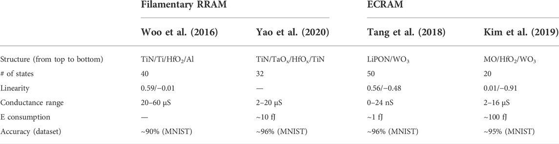
TABLE 1. Benchmark table showing synaptic update metrics for filamentary RRAM and ECRAM devices.
What is often neglected and has not yet been explored is the array E consumption, which considers not only the selected multiple ECRAM cells to be updated, but also the unselected ECRAM cells. Assuming certain three-terminal ECRAMs in the array are selectively updated, the gate-source voltage (VG) and source-drain voltage (VD) can be addressed to selected lines simultaneously based on the half-bias scheme (Kim et al., 2019), (Li et al., 2020), (Lee et al., 2021). Depending on the location of the adjacent unselected cells, VG or VD can be partially applied, thereby creating additional leakage paths consisting of gate-source current (IGS) or ISD. More importantly, since the ECRAM channel is normally on, the effect of ISD being greater than IGS (Kang and Woo, 2021) should be investigated.
Consequently, the aim of this study is to identify how the ISD is involved in E consumption in a large-sized ECRAM array. Based on experimentally obtained update behaviors in a 2 × 2 CuOx/HfOx/WOx ECRAM array, we investigated the effect of ISD on array size. Through case studies considering the location of selected ECRAM cells and sequential update (SU) direction, we showed the update method that minimize the involvement of the ISD for energy-efficient neuromorphic computing.
For the 2 × 2 array, four channels with a size of 50 × 50 μm2 were patterned by conventional lithography and lift-off methods. A 20-nm-thick WOx channel was deposited by RF sputtering at 50 W power with WO3 target on top of SiO2 substrate. For source and drain pads, W layers were formed at both edges of the WOx channel. Then, an electrolyte and a gate were sequentially deposited in the vertical direction of the WOx channel to connect each device. A 25-nm-thick HfOx serving as the electrolyte was deposited by RF sputtering with HfO2 target with power of 100 W in Ar plasma ambient. To limit the injection of mobile ions, a CuOx gate electrode formed by RF sputtering on a Cu metal target in Ar:O plasma gas, a ratio of 27:3 being used, as it was found to have been optimal in our previous work (Kang et al., 2022a). The fabricated ECRAM array was characterized using a B1500 semiconductor parameter analyzer and B1530A waveform generator/fast measurement unit.
Figure 1A represents the schematic diagram of a unit ECRAM device. The ISD of the ECRAM cell was measured by applying a VD to the drain and grounding the source. To update the ISD in the unit ECRAM cell (Kang et al., 2022b), a VG of +6 V (or −4 V) was applied for potentiation (or depression), respectively. The optical microscope image of a fabricated 2 × 2 ECRAM array was shown in Figure 1B. Notably, in the array—since the gate line (G1) is connected multiple ECRAM cells—the half-bias scheme (Kim et al., 2019), (Li et al., 2020), (Lee et al., 2021) can be exploited to address the full voltage to a selected cell, as well as to deactivate unselected cells. Unlike the unit cell operation, both a VG of +3 V and a VD of −3 V were applied to the G1 and D1 lines, respectively, as shown in the top of Figure 1C. This induced a total of +6 V as an effective VG to the selected cell during potentiation. Since the single G1 line was shared, the connected two cells can be simultaneously updated by applying −3 V to the D2 line as well. It is defined as a fully parallel update (PU) operation. In the same manner, for depression, a VG of −2 V and a VD of +2 V were applied. The effective VG of −4 V made to reduce the ISD. Note that the reason for using the half-bias scheme is to update only a certain ECRAM cell in the array. As shown in the bottom of Figure 1C, when 0 V was assigned to the D1 line, a half voltage of +3 V was induced at the VG, thereby suppressing the update of the cell due to the insufficient VG. Multiple ECRAMs can be thus updated cell-by-cell by changing the amplitude of VD to a specific D line, meaning the SU operation. Based on these measurement conditions, as VD of −3 V with a pulse width (tD) of 500 ms was addressed to D1 and D2 lines at the given VG of +3 V with a pulse width (tG) of 500 ms, the w11 and w12 were linearly updated in real-time (Figure 1D). Conversely, ISD was steadily decreased during depression, when a VG of −2 V tG of 500 ms and a VD of +2 V with a tD of 500 ms were successively applied. These resulted in the PU of w11 and w12 for the first 60 pulses. On the other hand, when only w11 was targeted to update, 0 V was applied to the D2. Since VG was solely applied to the unselected cell, negligible update of w12 was observed for the next 60 pulses due to insufficient voltage. The reversible PU and SU operations continued to be successfully observed.
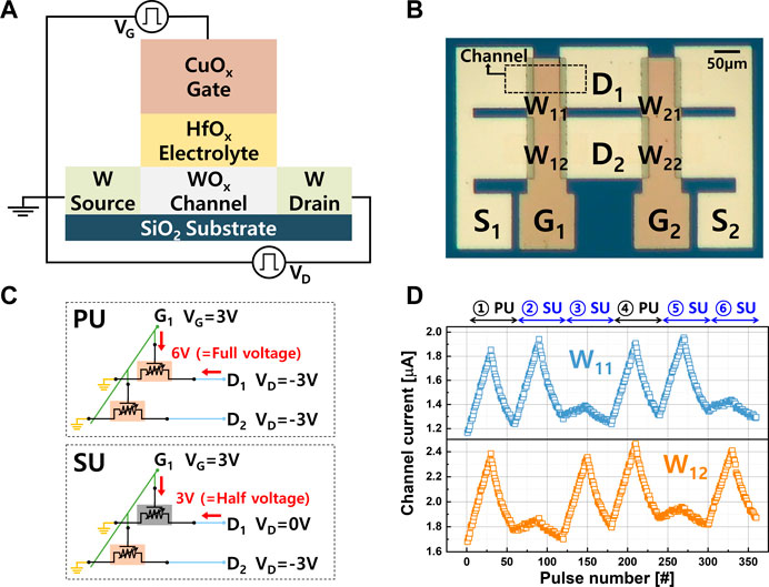
FIGURE 1. (A) Schematic diagram of unit ECRAM device and (B) optical microscopic image of the fabricated 2 × 2 ECRAM array. (C) Half-bias pulse conditions for PU and SU. (D) w11 and w12 can be simultaneously updated in parallel or sequential fashion.
We then analyzed the E consumed by each update operation. For ideal PU, all ECRAM cells can be assumed to be updated simultaneously. As VG and VD pulses are applied to all lines in parallel, the induced IGS and ISD from selected cells contributed to the E consumption (Figure 2A). The E consumption of one selected cell (Esel) consists of VG-related E (EG) and VD-related E (ED), which can be derived by as follows:
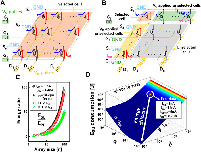
FIGURE 2. The schematic illustrations of (A) PU and (B) SU in n × n ECRAM array. Unlike the PU operation, where only selected cells are involved, four regimes in the array for SU are classified based on voltage conditions. (C) Calculated E ratio with respect to the array size. The ratio can be minimized by reducing ISD at a given IGS. (D) The three-dimensional plane graph showing ESU as a function of ISD and IGS.
For simplicity, the update operation in this study is defined as a change of ISD for potentiation from the pristine ECRAM. An IGS of 64 nA and ISD of 10.2 μA measured at effective full VG of +6 V and VD of −3 V were extracted from the experimental data. An EG and ED of 192 nJ and 15.3 μJ, respectively, were calculated. For an array size of n×n, the total E of PU (EPU) can be defined by multiplying the Esel by the number of cells (=n2) as follows:
Conversely, when n2 cells were sequentially updated in the array, leakage paths through neighboring cells that are partially biased needed to be considered. Specifically, a VG of +3 V addressed to the horizontal G1 line generates leakage sources through n−1 unselected cells in the S1 row apart from the selected cell, as shown in Figure 2B. These VG-induced leakage currents sink to the source (IGS,un) and drain (ISD,un) of 5 nA read at a VG of +3 V, thus inevitably producing E (EGS,un) as follows:
In the case of D1 column, it is noteworthy that a VD of -3 V causes ISD through n-1 unselected cells as well as the gate-drain leakage current (IGD,un). The E in the unselected area where VD is applied (ED,un) can be expressed as follows:
The remaining unselected cells can be ignored. Consequently, the E during SU can be derived as follows:
The calculations show that the SU compared to PU wastes considerable E due to these additional leakage paths, which is exacerbated in large scale arrays (Figure 2C). However, during the actual training stage in neuromorphic systems, at the expense of an inefficient E and latency drawback, the SU can be expected to be more frequently conducted rather than PU. To reduce the E during SU, we examined the E consumption by varying ISD of the ECRAM at a given IG, as shown in Figure 2C. This results in an alleviated E consumption as a function of reduced ISD. It can be further clarified by adjusting both ISD and IGS. As shown in Figure 2D, the ESU is more sensitive to ISD at the given experimental data, where both coefficients of α and β are 1. When β is substantially lowered through design of the ECRAM and its material stack (Melianas et al., 2022), (Lee et al., 2022), ESU savings for the 10 × 10 sized array can be achieved.
The impact of ISD and IGS,un (or IGD,un) on the ESU can be found directly by analyzing the weight update with respect to the locations of the selected cells, as shown in Figures 3A,B. In both cases, a single line of n cells is selected, but different types of voltage are applied to the unselected cell regimes (see the “patterned area”). Erow and Ecol can be defined as E when only a certain row and column are updated. For Erow (or Ecol), VD (or VG) pulses entering all column (or row) lines cause undesired leakages via n (n−1) unselected cells, inducing waste ED,un (or EG,un), respectively. Each E can be thus expressed as follows:
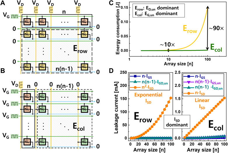
FIGURE 3. Single (A) row or (B) column is updated in the n × n array. (C) E consumption responds differently to the array size depending on the voltage applied to the unselected cell region. (D) Although ISD is dominant leakage component in both cases, the impact of ISD for Erow is substantial.
As shown in Figures 3, a noticeable E difference (of the order of 102 in the 100 × 100 sized array) can be observed. This can be explained by examining which leakage paths occurring in the unselected area are primarily involved as the array size increases, as shown in Figure 3D. Since the contribution of ISD exponentially increases with respect to the cell numbers for Erow, ISD prevails over other leakage components. Conversely, in the case of Ecol, ISD component is linearly proportional to the array size. Although the ISD seems to be dominantly served as a major leakage component, the impact of the ISD can be minimized for Ecol. These results imply that the energy efficiency can be enhanced by utilizing update methodologies that suppress the participation of the ISD via unselected cells as much as possible.
To identify a preferred update scheme, we conducted a case study, where the selected cells were randomly distributed in a 3 × 3 array, as shown in Figure 4A. The cells can be updated in two ways: column-by-column or row-by-row. Three steps of updates were sequentially executed, but different combinations of selected cells and unselected cells were assigned in each step (Figure 4B). Considering the first update step, D1 solely needed to be activated, while G1 and G3 were turned on during column-by-column scheme (top of Figure 4B). Thus, the IG,un was the primary leakage source through the rest of the columns. However, to update the same number of cells in a row-by-row fashion, G1 was turned on. Simultaneously, an additional VD was needed to be addressed through the D1 and D2 lines (bottom of Figure 4B). As a result, E loss occurred due to the considerable ISD from the unselected cell areas. When a few cells were updated in a row or column in the array, the E difference depending on the scheme became negligible because the participation of lines that produced leakages was reduced. Consequently, it turned out that the column-by-column scheme could enable energy efficiency twice as high as that of the row-by-row sequence, as shown in the E calculation with respect to update direction (Figure 4C).
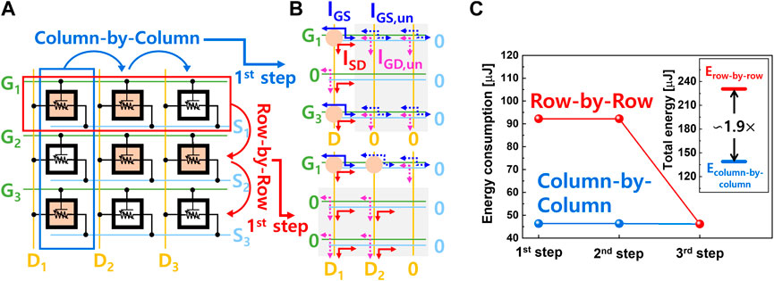
FIGURE 4. (A) 3 × 3 ECRAM array in which the cells to be updated are randomly distributed for the case study. (B) The leakage current components depending on the update scheme of the first step. (C) Calculated total E consumption for each update direction.
However, as we reported in our previous work (Woo and Yu, 2019), considering the actual array operation, parasitic components such as line resistance began to be involved. Particularly, as interconnect line was aggressively scaled or array sizes were increased, the impact of line resistance on the cell becomes more pronounced. This study based on the fabricated small-sized ECRAM array excluding external factors revealed one of the important leakage current components for a successful weight update operation, so further study is needed to verify the analysis. In this regard, we recently developed an ECRAM model to describe the observed synaptic behavior (Kim et al., 2022). We thus expect to conduct a comprehensive investigation of ECRAM arrays, taking into account non-ideal effects such as device reliability and parasitic resistance (or capacitance) on ECRAM model implemented in SPICE.
We experimentally demonstrated the PU and SU in a 2 × 2 CuOx/HfOx/WOx ECRAM array. Most studies have reported a low E of the ECRAM unit cell by simply considering the IGS. However, our findings revealed that the inevitable ISD through neighboring cells—which had been neglected in studies to date—plays a crucial role in E consumption at the array-level. This is because VG and VD are partially applied to the lines to selectively update specific cells in the array, generating unavoidable leakage sources. It should be noted that since the ECRAM performed normally, the E consumption was more sensitive to ISD. This was further mathematically validated by examining the impact of VG (or VD) applied to unselected cells as a function of the array size. The results showed that lowering the ISD of the ECRAM achieved through material and device engineering was the preferred approach. In addition to this ECRAM unit cell point of view, we showed that the SU scheme using a column-by-column approach, in which a smaller ISD,un involvement could be derived using fewer activated column lines, can further reduce E consumption.
The original contributions presented in the study are included in the article/Supplementary Material; further inquiries can be directed to the corresponding author.
HK experimented and characterized the devices. HK, NK, and SJ performed the calculations. HK, NK, SJ, HWK, EH, SK, and JW discussed the electrical results. SK suggested the guidelines. JW contributed ideas and supervised the study. HK and JW wrote the manuscript.
This work was supported by the National Research Foundation (NRF) grant funded by the Korea government (MSIT) (NRF-2020M3F3A2A01081775, NRF-2021R1C1C1003261, and NRF-2022R1A2C2012603). This research was supported by the MSIT (Ministry of Science and ICT), Korea, under the ITRC (Information Technology Research Center) support program (IITP-2022-RS-2022-00156225) supervised by the IITP (Institute for Information and Communications Technology Planning and Evaluation).
The authors declare that the research was conducted in the absence of any commercial or financial relationships that could be construed as a potential conflict of interest.
All claims expressed in this article are solely those of the authors and do not necessarily represent those of their affiliated organizations, or those of the publisher, the editors and the reviewers. Any product that may be evaluated in this article, or claim that may be made by its manufacturer, is not guaranteed or endorsed by the publisher.
Burgt, Y., Lubberman, E., Fuller, E. J., Keene, S. T., Faria, G. C., Agarwal, S., et al. (2017). A non-volatile organic electrochemical device as a low-voltage artificial synapse for neuromorphic computing. Nat. Mat. 16 (4), 414–418. doi:10.1038/nmat4856
Burr, G. W., Shelby, R. M., Sebastian, A., Kim, S., Kim, S., Sidler, S., et al. (2017). Neuromorphic computing using non-volatile memory. Adv. Phys. X 2 (1), 89–124. doi:10.1080/23746149.2016.1259585
Fuller, E. J., Gabaly, F. E., Leonard, F., Agarwal, S., Plimpton, S. J., Jacobs-Gedrim, R. B., et al. (2017). Li-ion synaptic transistor for low power analog computing. Adv. Mat. 29 (4), 1604310. doi:10.1002/adma.201604310
Kang, H., Kim, H. W., Hong, E., Kim, N., and Woo, J. (2022). “Linear and symmetric weight update of CuOx/HfOx/WOx ECRAM synapse for neuromorphic systems,” in IEEE Silicon Nanoelectronics Workshop, Honolulu, HI, USA, 11-12 June 2022.
Kang, H., Kim, H. W., Hong, E. R., and Woo, J. (2022). Analog synaptic behavior of mobile ion source-limited electrochemical RAM using CuOx oxide electrode for deep learning accelerator. Appl. Phys. Lett. 120 (12), 122101. doi:10.1063/5.0086164
Kang, H., and Woo, J. (2021). Cu-ion-actuated three-terminal neuromorphic synaptic devices based on binary metal-oxide electrolyte and channel. Appl. Phys. Lett. 119 (7), 072103. doi:10.1063/5.0059697
Kim, N., Kang, H., Kim, H. W., Hong, E., and Woo, J. (2022). Understanding synaptic characteristics of nonvolatile analog redox transistor based on mobile ion-modulated-electrolyte thickness model for neuromorphic applications. Appl. Phys. Lett. 121 (7), 072105. doi:10.1063/5.0099827
Kim, S., Todorv, T., Onen, M., Gokmen, T., Bishop, D., Solomon, P., et al. (2019). “Metal-oxide based, CMOS-compatible ECRAM for deep learning accelerator,” in IEEE International Electron Devices Meeting (IEDM), San Francisco, CA, USA, 07-11 December 2019.
Lee, C., Rajput, K. G., Choi, W., Kwak, M., Nikam, R. D., Kim, S., et al. (2020). Pr0.7Ca0.3MnO3-Based three-terminal synapse for neuromorphic computing. IEEE Electron Device Lett. 41 (10), 1500–1503. doi:10.1109/led.2020.3019938
Lee, J., Nikam, R. D., Kwak, M., and Hwang, H. (2022). Strategies to improve the synaptic characteristics of oxygen-based electrochemical random-access memory based on material parameters optimization. ACS Appl. Mat. Interfaces 14 (11), 13450–13457. doi:10.1021/acsami.1c21045
Lee, J., Nikam, R. D., Kwak, M., Kwak, H., Kim, S., and Hwang, H. (2021). Improvement of synaptic properties in oxygen-based synaptic transistors due to the accelerated ion migration in sub-stoichiometric channels. Adv. Electron. Mat. 7 (8), 2100219. doi:10.1002/aelm.202100219
Li, Y., Lu, J., Shang, D., Liu, Q., Wu, S., Wu, Z., et al. (2020). Oxide-based electrolyte-gated transistors for spatiotemporal information processing. Adv. Mat. 32 (47), 2003018. doi:10.1002/adma.202003018
Mead, C. (1990). Neuromorphic electronic systems. Proc. IEEE 78 (10), 1629–1636. doi:10.1109/5.58356
Melianas, A., Kang, M., Mohammadi, A., Quill, T. J., Tian, W., Gogotsi, Y., et al. (2022). High-speed ionic synaptic memory based on 2D titanium carbide. MXene 32 (12), 2109970.
Roy, K., Jaiswal, A., and Panda, P. (2019). Towards spike-based machine intelligence with neuromorphic computing. Nature 575, 607–617. doi:10.1038/s41586-019-1677-2
Tang, J., Bishop, D., Kim, S., Copel, M., Gokmen, T., Todorov, T., et al. (2018). “ECRAM as scalable synaptic cell for high-speed, low-power neuromorphic computing,” in IEEE International Electron Devices Meeting (IEDM), San Francisco, CA, USA, 01-05 December 2018.
Woo, J., Moon, K., Song, J., Lee, S., Kwak, M., Park, J., et al. (2016). Improved synaptic behavior under identical pulses using AlOx/HfO2 bilayer RRAM array for neuromorphic systems. IEEE Electron Device Lett. 37 (8), 994–997. doi:10.1109/led.2016.2582859
Woo, J., and Yu, S. (2019). Impact of selector devices in analog RRAM-based crossbar arrays for inference and training of neuromorphic system. IEEE Trans. VLSI. Syst. 27 (9), 2205–2212. doi:10.1109/tvlsi.2019.2917764
Woo, J., and Yu, S. (2018). Resistive memory-based analog synapse: The pursuit for linear and symmetric weight update. IEEE Nanotechnol. Mag. 12 (3), 36–44. doi:10.1109/mnano.2018.2844902
Keywords: neuromorphic system, synaptic device, ECRAM array, weight update, energy consumption
Citation: Kang H, Kim N, Jeon S, Kim HW, Hong E, Kim S and Woo J (2022) Analysis of electro-chemical RAM synaptic array for energy-efficient weight update. Front. Nanotechnol. 4:1034357. doi: 10.3389/fnano.2022.1034357
Received: 01 September 2022; Accepted: 10 October 2022;
Published: 25 October 2022.
Edited by:
Ying-Chen Chen, Northern Arizona University, United StatesCopyright © 2022 Kang, Kim, Jeon, Kim, Hong, Kim and Woo. This is an open-access article distributed under the terms of the Creative Commons Attribution License (CC BY). The use, distribution or reproduction in other forums is permitted, provided the original author(s) and the copyright owner(s) are credited and that the original publication in this journal is cited, in accordance with accepted academic practice. No use, distribution or reproduction is permitted which does not comply with these terms.
*Correspondence: Jiyong Woo, aml5b25nLndvb0BrbnUuYWMua3I=
Disclaimer: All claims expressed in this article are solely those of the authors and do not necessarily represent those of their affiliated organizations, or those of the publisher, the editors and the reviewers. Any product that may be evaluated in this article or claim that may be made by its manufacturer is not guaranteed or endorsed by the publisher.
Research integrity at Frontiers
Learn more about the work of our research integrity team to safeguard the quality of each article we publish.