 Yann Beilliard1,2*
 Fabien Alibart2,3
- 1Institut Interdisciplinaire d′Innovation Technologique (3IT), Université de Sherbrooke, Boulevard de l'Université, Sherbrooke, QC, Canada
- 2Laboratoire Nanotechnologies Nanosystèmes (LN2)–CNRS, Université de Sherbrooke, Boulevard de l’Université, Sherbrooke, QC, Canada
- 3Institute of Electronics, Microelectronics and Nanotechnology (IEMN), Université de Lille, Villeneuve d'Ascq, France
Neuromorphic computing based on spiking neural networks has the potential to significantly improve on-line learning capabilities and energy efficiency of artificial intelligence, specially for edge computing. Recent progress in computational neuroscience have demonstrated the importance of heterosynaptic plasticity for network activity regulation and memorization. Implementing heterosynaptic plasticity in hardware is thus highly desirable, but important materials and engineering challenges remain, calling for breakthroughs in neuromorphic devices. In this mini-review, we propose an overview of the latest advances in multi-terminal memristive devices on silicon with tunable synaptic plasticity, enabling heterosynaptic plasticity in hardware. The scalability and compatibility of the devices with industrial complementary metal oxide semiconductor (CMOS) technologies are discussed.
Introduction
For artificial intelligence (AI) applications, traditional computer hardware based on the serial von Neumann architecture suffers from a major performance and energy-efficiency problem, mainly due to the massive data transfer between processing and memory units. One promising way to overcome this so-called von Neumann bottleneck is to embrace computational neuroscience and neuromorphic engineering paradigms to create parallelized spike-based computing systems (Yang et al., 2020). In that scope, emerging two-terminal resistive memories (i.e., memristors) are considered as key building blocks, owing to their controllable conductance state which can be used to encode synaptic weights (Li and Ang, 2021). The main synaptic-like behaviors reported to date include short- and long-term memory (STM/LTM), paired-pulse facilitation (PPF) and depression (PPD), spike-timing-dependent plasticity (STDP), spike-rate-dependent plasticity (SRDP) and metaplasticity (Zhu et al., 2020).
The two-terminal architecture of typical memristive devices can only authorize the emulation of homosynaptic plasticity–input-specific changes at synapses directly involved in a pre-synaptic activation. Hence, most of the studies done on memristor-based spiking neural networks (SNN) rely solely on Hebbian-type learning rules (e.g., STDP) based on homosynaptic plasticity (Chua et al., 2019). Such SNNs are prone to weight saturation (i.e., runaway dynamics) and are devoid of synaptic competition, which can weaken network representativity due to overexcitability or silencing of neurons (Moser and Moser, 1999; Chen et al., 2013). These phenomena are usually at the source of poor learning and computing performance. Recent advances in neuroscience have demonstrated that synaptic plasticity in biological neural networks is regulated not only by homosynaptic plasticity, but also by synaptic interactions (competition, cooperation) and more importantly heterosynaptic plasticity–modulatory input-dependent changes at inactive synapses related to strong post-synaptic activities (Bailey et al., 2000; Chistiakova et al., 2014). These complex heterosynaptic behaviors, which can be mediated by limited available energy and modulatory cells (e.g., astrocyte and interneurons, see Figure 1A), play an important role in the stabilisation and memory functions of neural systems. They are indeed responsible for the normalization of all synaptic weights connected to a neuron, meaning that the total weight remains constant. Such regulation mechanisms strongly limit the risk of synaptic weights to saturate, and thus contribute to improve the learning capability and computing performance of the network. Therefore, it appears that homosynaptic and heterosynaptic plasticity mechanisms have complementary computational properties at different spatiotemporal scales that could be beneficial for neuromorphic systems.
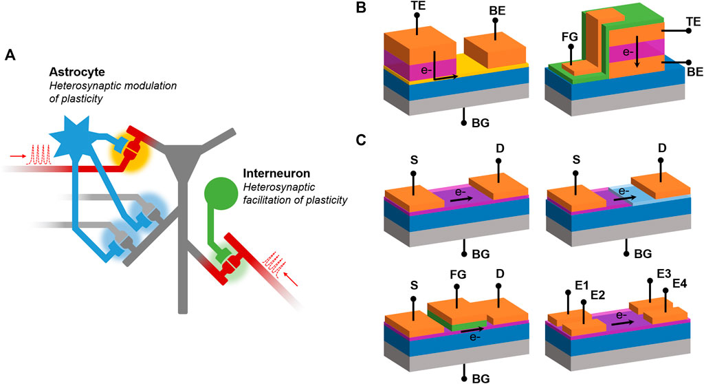
FIGURE 1. (A) Schematic representations of spiking activities between neurons, modulated by an astrocyte and an interneuron. Homosynaptic plasticity occurs at synapses directly involved in a pre-synaptic activation (red connections). An astrocyte can induce heterosynaptic plasticity modulation in distant inactive synapses (blue areas) based on local synaptic activities (yellow area). An interneuron can act as an intermediate cell responsible for heterosynaptic facilitation (green area). (B, C) Schematic representations of recently reported artificial synapses based on emerging multi-terminal vertical and planar memristive devices, featuring resistive switching materials (transparent purple) and electrodes (orange). (B) Typical vertical multi-terminal devices, where the modulation electrode is implemented either by the substrate as a back gate (BG) or a top gate (TG) separated from the switching materials by a dielectric layer (green). The top electrode (TE) and the bottom electrode (BE) are placed at different altitudes, and both the switching mechanisms and the electronic current (e-) are vertical. (C) Various architectures of planar multi-terminal devices where the switching mechanisms and the electronic current are parallel to the substrate. In a memtransistor architecture, two electrodes are used as source (S) and drain (D), and the switching modulation is done using a back gate and/or a front gate. In this case, the switching medium can be composed of either a single material or an heterostructure combining different types of materials placed on top of each other or side-by-side. Other works also involve devices with multiple electrodes fabricated on top of the switching material, allowing to implement synaptic interactions.
In recent years, the use of heterosynaptic plasticity in software SNNs has resulted in improved learning capabilities (Susi et al., 2018; Daram et al., 2020). The implementation of an astrocyte-reinforced STDP has also been reported in Intel’s Loihi neuromorphic chip (Tang et al., 2019). Going forward, improving the online learning capabilities, the speed and the energy efficiency of future bio-inspired computing systems will require novel neuromorphic hardware that natively emulate both homo- and heterosynaptic plasticity mechanisms. For this reason, multi-terminal memristive devices have attracted a lot of attention lately due to their tunable and rich resistive switching dynamics at various time scales, enabled by the interplay of local modulatory voltage signals and complex nanostructures based on emerging materials. Indeed, outside from the two terminals that are required to perform resistive switching, the additional terminals can be used as gates to control the electric field across the switching materials, resulting in a modulation of the switching dynamics similar to heterosynaptic plasticity. This feature opens new opportunities to implement in hardware desirable advanced bio-inspired learning rules and global regulation mechanisms. Moreover, additional terminals can also be used as active electrodes allowing to decouple the reading and programing processes, otherwise impossible with 2-terminal devices. This mechanism combined with gate tuning could offer better control over the switching linearity and symmetry, recently identified as key factors in efficient neuromorphic hardware (Burr et al., 2015; Xiao et al., 2020). Using multiple active electrodes also provides the possibility to go beyond the single synaptic element by implementing in a single device multiple artificial synapses capable to interact with each other. Finally, multi-terminal devices enable to engineer multiple input/output components, thus increasing the fan-in/fan-out at the device level without requiring complex interconnections or circuit overhead. As depicted in Figures 1B,C, both vertical and planar multi-terminal architectures are currently investigated with the goal to mimic complex plasticity mechanisms such as heterosynaptic plasticity and synaptic interactions between multiple electrodes.
In this mini-review, our aim is to provide a brief overview of the latest progress in multi-terminal memristive devices paving the way for the hardware implementation of both homo- and heterosynaptic plasticity. We will focus our analysis of the reported studies in the light of their compatibility with industrial complementary metal oxide semiconductor (CMOS) technologies. The compatibility of multi-terminal memristive devices with the semiconductor industry is indeed of major importance for future endeavors aiming to develop truly scalable low-power high-performance neuromorphic systems. As such, this article specifically targets inorganic solid-state memristive devices fabricated on silicon substrate having the potential to be co-integrated with CMOS circuits. This article will first outline multi-terminal devices with a vertical architecture, before reviewing planar devices. For both sub-sections, reported works include memristors and memtransistors based on metal oxides, nanoparticles, nanowires, 2D materials and heterostructures. The last part of this article will discuss future research opportunities and development directions aiming to tackle challenges related to CMOS-compatible fabrication, device performance and scalability.
Multi-Terminal Devices as Tunable Artificial Synapses
This section reviews the state-of-the-art of vertical and planar memristive devices with three or more terminals enabling tunable synaptic plasticity and synaptic interactions. As shown in Figures 1B,C, devices are classified as vertical (planar) when the switching mechanisms and the electronic current are perpendicular (parallel) to the substrate. All devices reviewed are summarized in Table 1.
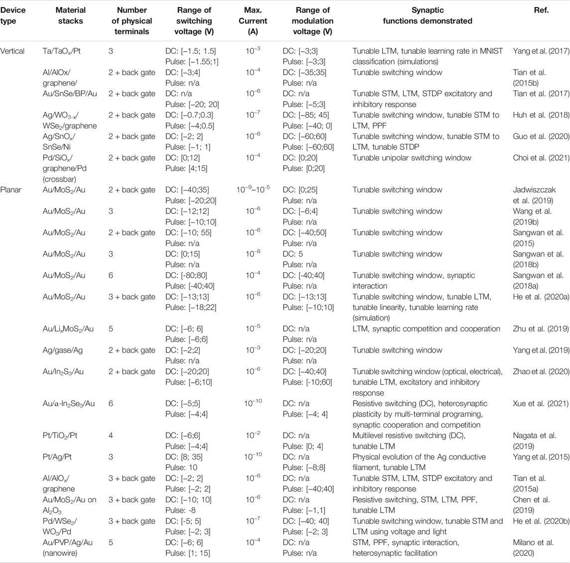
TABLE 1. Summary of reported multi-terminal vertical and planar memristive devices.
Vertical Devices
(Yang et al., 2017) reported a three-terminal oxide-based memristive device where the conventional two-terminal synapse was based on a Ta/TaOx/Pt structure, while a Pt/Ti side electrode was used as a modulatory electrode. A similar three-terminal architecture was investigated by (Herrmann et al., 2018), with the specificity of having the SrTiO3-based active layer being deposited on the side of the top and bottom electrodes. However, only (Yang et al., 2017) used this architecture to modulate the migration dynamics of the oxygen vacancies in the active layer to achieve tunable LTM. Synaptic facilitation/depression was reported using modulation voltage of up to 3 V. Interestingly, the switching non-linearity and asymmetry typically observed in oxide-based devices (Wang C. et al., 2019) was noticeably improved for specific gate voltages. This suggests that additional terminals could be used as gates specifically employed to compensate switching non-idealities. However, a slight difference in switching dynamics was noticed depending on the sign of the modulation voltage, suggesting non-uniformity in the distribution of the enhanced electric field. This result indicates that various modulation gate geometries should be explored in future studies in order to improve the control over the switching modulation and thus the switching linearity and symmetry. Finally, in-memory Boolean logic and simulations of MNIST classification (machine learning) were reported. In the latter case, the modulation gate was used as a mean to dynamically change the learning rate, paving the way for both accelerated learning and higher accuracy.
Other reported works involve the use of 2D materials and heterostructures. In 2015, a three-terminal device based on graphene combining a transistor and a memristor was proposed by (Tian et al., 2015b). The active layer was made of a 5 nm thick native aluminum oxide (AlOx) formed at the interface between an aluminum-based top electrode and the graphene layer used as a bottom electrode. The resistive switching behavior, attributed to the formation of a conductive filament (CF) made of oxygen vacancies in the AlOx layer, was modulated by applying a voltage on the back gate (i.e., the Si substate) ranging from −35 to 35 V. In doing so, the resistive switching window could be tuned thanks to the band gap opening in the bilayer graphene. Another work published by (Tian et al., 2017) reported both excitatory and inhibitory synaptic behavior in a vertical two-terminal device where the back gate acted as a modulation terminal. The device consisted in a heterojunction formed by black phosphorus (BP) and tin selenide (SnSe) deposited by exfoliation on SiO2. A phosphorus oxide (POx) was intentionally formed between the BP and SiO2 layers to act as an electron trap. The interplay between the charge transfer at the BP/POx interface and the back-gate-tunable electronic properties of the SnSe/BP heterojunction gave rise to reconfigurable synaptic characteristics capable of excitatory or inhibitory responses for positive and negative gate voltage respectively. Interestingly, the switching dynamics was almost linear only using negative pulses, for both positive and negative modulation voltages. Further exploration of heterostructures was done by (Huh et al., 2018), with a synaptic device consisting in a vertical Ag/WO3-x/WSe2/graphene architecture. While the WO3-x served as the main memristive layer, the WSe2/graphene heterojunction acted as a gate-controlled Schottky barrier, so-called the “barristor”. Advanced synaptic functions were successfully emulated, including STM, LTM and PPF. The use of large modulation voltages of up to 85 V allowed to tune the switching windows in DC mode. For pulse measurement, modulation voltages in the range of 40 V allowed to demonstrate a transition from STM to LTM, with noticeable switching non-linearity and asymmetry.
More recently (Guo et al., 2020), reported a vertical Ag/SnOx/SnSe/Ni memristor fabricated using a van der Waals (vdW) metal-integration approach. Although this fabrication process (Liu et al., 2019) is not yet fully scalable and compatible with conventional semiconductor technologies, it allowed the authors to peel off the Ag top electrodes from a SiO2 substrate with a PMMA film to then deposit them on top of 2D SnSe through a dry-transfer process without damaging the SnOx-based switching junction. A 100% fabrication yield was achieved with this method relying on the weak adhesion force between Ag and SiO2. The fabricated devices exhibited promising endurance and retention performance, where the formation of Ag filaments in the SnOx layer was identified as the main switching mechanisms. In terms of synaptic behavior, tunable STM, STM to LTM and STDP were demonstrated with a modulation voltage of up to 60 V on the back gate. However, the duration of the programing voltage pulses was in the range of seconds, which would cause serious performance issues in the case of hardware-implemented neural networks. Finally (Choi et al., 2021), have recently demonstrated the first crossbar integration of back-gated memristors made of SiOx/graphene bi-layer. The 16 × 16 memristor array was used to implement non-volatile universal logic gates. Along with all the other vertical devices discussed in this section, this demonstration represents a step towards a scalable hardware implementation of neuromorphic computing leveraging tunable synaptic plasticity.
Planar Devices
Single Structures
Recent advances in nanofabrication and material synthesis have allowed numerous groups to explore the use of emerging 2D materials as a resistive switching medium for planar multi-terminal synaptic devices. The atomically thin geometry of 2D materials presents multiple advantages in terms of scalability, electrical tunability and low energy consumption. In recent years, one of the most studied 2D materials for tunable neuromorphic functions is molybdenum disulfide (MoS2). In monolayer MoS2 with defects, sulfur vacancies can act as electron donors which can promote the migration of ions and the formation of CFs made of active metal atoms provided by electrodes (Wang et al., 2020). In addition to its atomic scalability, this transition metal dichalcogenide offers fast charge carrier dynamics (Hong et al., 2014) and tunable electronic, optoelectronic and electrochemical properties (Radisavljevic et al., 2011; Mak and Shan, 2016) which can be leveraged to implement multi-gated neuromorphic devices (John et al., 2018; Jadwiszczak et al., 2019).
For synaptic applications, Sangwan et al. proposed gate-tunable memtransistor devices made of polycrystalline monolayer MoS2 with various configurations: two terminals and a back gate (Sangwan et al., 2015), three terminals including a top gate (Sangwan et al., 2018b) and six terminals with a back gate (Sangwan et al., 2018a). In their seminal work of 2015, the use of the back gate enabled tunable resistive switching windows with DC voltage sweeps using a modulation voltage ranging from −50 to 55 V (Sangwan et al., 2015). In this case, it was demonstrated that the memristive phenomena was mediated by the grain boundaries (GB) of the single-layer MoS2. In particular, it was observed that the gate-tuning could result in a proportional shift of the switching voltage Vset or the resistance range depending on whether the MoS2 layer had an intersecting GB or a bisecting GB respectively. It was noted that these features could provide flexibility in the design of fault-tolerant architectures and be useful to mitigate impedance matching challenges. The top-gated architecture used in (Sangwan et al., 2018b) employed a MoS2 layer with several grain boundaries which exhibited both transistor and memristor characteristics. The integration of the top gate allowed to divide by 10 the required voltage to observe modulation compared to the back-gated devices. Low gate voltage in the range of a few volts were also observed by (Wang L. et al., 2019) in the case of MoS2-based device with a top gate and HfO2 as gate insulator. Regarding the six-terminal devices (Sangwan et al., 2018a), this configuration allowed to implement multiple synapses in a single device. LTM with significant non-linearity and asymmetry was reported, as well as STDP using voltage pulses in the range of 40 V. Interestingly, synaptic interactions were achieved by increasing (decreasing) the conductance of the MoS2 using the most distant terminals of the 6-terminal configuration, which induced an increase (decrease) of conductance between the inner terminals. This type of synaptic modulation could be used to implement a form of cooperative heterosynaptic plasticity at the device level, providing opportunities for novel learning rules at the network level.
Another group have successfully fabricated a dual-gated device based on exfoliated MoS2 (He C. et al., 2020). Using h-BN as a gate dielectric, versatile synaptic behavior was shown including tunable resistive switching window and LTM. The impact of the gate voltage on the switching dynamics was specifically studied, revealing that the non-linearity could be reduced by applying a positive modulation voltage at the cost of a reduced ON/OFF ratio. The opposite behavior was observed for negative modulation voltages, where the non-linearity and ON/OFF ratio increased exponentially. Authors have also reported simulation results indicating that a better MNIST classification accuracy could be obtained by using a modulation voltage comprised between −5 and 5 V. Zhu et al. (2019) have explored the use of exfoliated LixMoS2 to fabricate a five-terminal planar device. The switching mechanisms was attributed to the transition of MoS2 between the 2H (semiconductor) and 1T’ (metal) phases induced by an increase/decrease in the local Li+ ion concentration. Three- and five-terminal configurations were used to demonstrate synaptic competition and cooperation. The competition was driven by the limited amount of Li+ ions in the LixMoS2 film between two connected synapses. For cooperation, the five-terminal architecture allowed to observe that the potentiation (depression) of one synapse induced the potentiation (depression) of the four others. For both configurations, the switching dynamics was highly non-linear and asymmetric, which must be addressed for future synaptic applications.
Other 2D materials than MoS2 were also explored for planar devices. Yang et al. (2019) have used layered GaSe nanosheets to fabricate a three-terminal synaptic device, exhibiting back-gate-tunable non-volatile switching using a low electric field of 3.3 × 10² V cm−1. The latter was attributed to the low migration energy of the intrinsic Ga vacancy in p-type gase. However, the relatively high switching voltage (∼V) and current level (∼mA) suggest that integration optimisations remain to be done to employ this type of device in low-power applications. Another gate-tunable synaptic device was reported by (Zhao et al., 2020) where the switching junction was made of non-layered In2S3 flakes. The latter were deposited by chemical vapor deposition (CVD), which required a thermal treatment of 980°C for 20 min. One can note that such temperature is not compatible with industrial back-end-of-line (BEOL) processes limited to 400°C. Nevertheless, both tunable switching window and LTM were demonstrated with either optical or electrical modulation using the substrate as a back gate. As observed in other studies, the switching non-linearity increased with the modulation voltage. Interestingly, depending on the back gate polarity, the device was either potentiated or depressed without changing the input pulse polarity. This controllable excitatory or inhibitory response is similar to what was observed in vertical SnSe-based devices by (Tian et al., 2017).
More recently, memristive devices based on ferroelectric switching α-In2Se3 were reported by (Xue et al., 2021). A six-terminal architecture was proposed, enabling multiple biasing configurations for both non-volatile DC switching and pulse programing. The required pulse duration was in the range of seconds, which would be redhibitory for a large-scale neuromorphic system. Nevertheless, synaptic interaction was observed as the modification of conductance between a pair of electrodes induced a change of conductance between remote pairs of electrodes. A three-terminal configuration was used to demonstrate non-linear synaptic change induced by the third electrode, as well as synaptic cooperation and competition by sending voltage pulses in 2 independent electrodes. The possibility to use one or two electrodes to directly change the conductance of the device allows to decouple the read and write processes. This feature is complementary to the gate-assisted tuning of plasticity. In the future, combining these two mechanisms would grant even more flexibility and control in the switching dynamics, enabling richer synaptic functions in hardware.
Only a few studies have reported heterosynaptic plasticity on planar devices without using 2D materials. Nagata et al. (2019) have employed rutile TiO2–x single crystal for thin film memristive planar devices with a four-terminal architecture. The multi-terminal device relied on field-induced oxygen vacancies migration to implement gate-tunable gradual and almost linear LTM with a very low cycle-to-cycle variability. The use of 2 electrodes for pulse programming and the other 2 electrodes as modulation gates allowed to improve the endurance and to tune the switching dynamics. Although these results are promising, the long voltage pulse in the range of seconds, the low resistance in the range of a hundred Ohms and the high temperature treatment of 700°C required to fabricate the TiO2–x layer currently prevent the use of such devices in an actual large-scale system. Another interesting approach explored by (Yang et al., 2015) consisted in a device where the switching layer was made of Ag nanoclusters deposited on a dielectric material. A four-terminal architecture demonstrated the physical evolution of the CF formed from the nanoclusters depending on the direction of the electric field between the Pt electrodes. Furthermore, a three-terminal version of the device where the third terminal was used as a modulation gate allowed to implement heterosynaptic facilitation and depression. However, the combination of abrupt and somewhat non-monotonic synaptic responses, ultra-low current levels (∼pA) and high switching voltage (∼10 V) calls for further development to render such devices compatible with operation conditions of CMOS technologies.
Heterostructures
The use of heterostructures combining the optical and electrical properties of different materials is another promising approach to design multi-terminal neuromorphic devices with synaptic functions tailored for specific applications. Several groups have thus recently explored vertical et lateral heterostructures made of dielectric thin films and 2D materials to implement complex synaptic behaviors. Building upon their work in (Tian et al., 2015b), (Tian et al., 2015a) have investigated a Al/AlOx/graphene architecture. The conductance of the device could be modified by trapping carriers from the graphene inside the AlOx layer by applying voltage pulses on the top gate. The modulation of STM, LTM and STDP was demonstrated by applying a constant voltage on the Si substrate used as back gate. Interestingly, the non-linear switching dynamics could be reversed depending on the polarity and amplitude of the back gate voltage. As in (Tian et al., 2017), this phenomenon enabled the use of such devices as either excitatory or inhibitory synapses. Chen et al. (2019) also used graphene in a four-terminal memristive vdW heterostructure combining MoS2 and h-BN exfoliated on a Al2O3 thin film. Authors managed to implement synaptic plasticity at various time scales using a dual-gate approach. In this case, the top gate was used for both resistive switching and synaptic plasticity modulation induced by voltage pulses coming from the back gate. He H.-K. et al. (2020) have also developed a dual-gated device based on a lateral heterostructure composed of 2D WSe2 and WO3. They successfully implemented tunable switching window, STM and LTM with remarkable linearity and symmetry. While the post synaptic current was driven by the so-called source and drain electrodes, the synaptic plasticity was modulated by both electrical and optical signals applied to the back gate and top side of the device, respectively. The switching mechanism was attributed to the injection/extraction of protons in the WO3 layer, which can be electrostatically tuned. The response to visible light of the device was explained by the creation of photogenerated holes in the WSe2 2D material upon illumination. The use of multiple modulation gates using different physical mechanisms offers a higher degree of control over the synaptic plasticity, which could prove useful for neuromorphic optoelectronic systems. Finally, another approach based on Ag nanowires with an insulating shell made of polyvinylpyrrolidone (PVP) was explored by (Milano et al., 2020) to fabricate a memristive network exhibiting advanced synaptic plasticity behavior. Using multiple terminals connected on the edge of the nanowire network, authors demonstrated that the device could emulate multiple synaptic connections and pathways showing resistive switching, STM, PPF and heterosynaptic facilitation.
Discussion and Perspectives
The growing necessity to implement advanced synaptic functions in neuromorphic hardware has pushed several groups to explore novel multi-terminal memristive devices based on metal oxides, nanoparticles, nanowires and 2D materials. Rich and tunable synaptic-like behaviors have been demonstrated, including short- and long-term heterosynaptic plasticity as well as synaptic interactions. Lately, 2D materials such as graphene, SnSe, MoS2, WSe2, GaSe and In2Se3 have emerged as promising candidates owing to their atomic-level thickness and tunable electronic properties that offer lower energy consumption and improved synaptic emulation. Although these demonstrations contribute to bridging the gap between software and hardware in the field of neuromorphic engineering, major challenges remain in terms of materials, device operation conditions, design and integration with CMOS technologies.
Materials and scalable fabrication processes compatible with CMOS technologies have to be investigated. Outside from memristive devices based on oxide thin films (Yang et al., 2017; Nagata et al., 2019), most demonstrations involve 2D materials which rely on fabrication processes that are not scalable such as exfoliation process (Yang et al., 2019; Zhu et al., 2019) or patterning with focused ion beam (Jadwiszczak et al., 2019). Some works employed wafer-level chemical vapor deposition (CVD), but the required thermal treatment is way above 400°C (Sangwan et al., 2018a; Wang L. et al., 2019; Zhao et al., 2020) which makes this approach still incompatible with CMOS processes. Ideally, developing industrial-grade deposition processes of 2D materials should result in well controlled atomically thin layers of perfectly arranged structures at the wafer level. This should lead to a significant reduction of cycle-to-cycle and device-to-device variability problems, which are still not solved in the case of conventional oxide-based memristive materials prone to defects and contaminant issues. Another important aspect of current studies is the overabundant use of Au and Pt as electrodes. The use of inert materials readily available in semiconductor foundries (e.g., TiN, W) should be investigated, as well as their impact on resistive switching mechanisms.
Regarding switching operations, reported devices relying on a back gate to modulate the switching operations necessitate gate voltage in the range of tens of volts. Planar devices based on 2D materials can also exhibit very high switching voltages, with values ranging from 20 to 80 V (see Table 1). For tunable memristive devices to be co-integrated with CMOS technologies, breakthroughs in fabrication and materials engineering remain to be made for the operation conditions to be in the range of a few volts. For example, as shown in some studies (Yang et al., 2017; Sangwan et al., 2018b), the integration of the modulation electrode as a top/side gate instead of a back gate can reduce the required voltage by an order of magnitude. Advanced designs such as gate-all-around architecture could potentially improve further the control on synaptic modulation.
In terms of scalable integration, one important milestone is to achieve the integration of synaptic devices into a fully connected network. In that aspect, further work has to be done to convert current planar devices into vertical multi-terminal memories. The vertical architecture indeed allows the fabrication of crosspoint structures, which provide the highest integration density when interconnected into a crossbar array. Furthermore, vertical integration opens new perspectives for monolithic 3D integration. In fact, conventional 2D integration requires complex interconnection layouts to mimic the parallel structure of the brain. Integrating multiple input/output at the device level and taking advantage of 3D interconnects with both lateral and vertical access lines (Xue et al., 2021) could help relaxing the important limitation of todays hardware for neuromorphic engineering. To this day, only one group has reported the fabrication of crossbar arrays of vertical multi-terminal memories using a combination of SiO thin film and graphene as electrode (Choi et al., 2021). However, some concerns exist regarding the compatibility of emerging memristive materials with high-density integrations. On the one hand, conventional memristive thin films are well suited for a vertical integration owing to their isotropic resistive switching mechanisms and improved performance at lower scale. On the other hand, 2D materials exhibit anisotropic memristive properties, resulting in different behaviors between in-plane (planar integration) or out-of-plane (vertical integration) resistive switching. Furthermore, a vertical integration could prevent the use of photonic or optoelectronic properties for resistive switching or modulation methods. These aspects should therefore be taken into account when determining the type of integration for a specific application using a certain type of 2D material. In that scope, innovative high-density integration schemes should be investigated for 2D materials. For example, a 3D integration taking inspiration from vertical random-access memories (VRAM) and the work of (Herrmann et al., 2018) demonstrating a vertical switching junction driven by two planar electrodes could result in promising stackable architectures.
Some groups have started to investigate the benefits of gate-tunable plasticity in neural network simulations, reporting the ability to optimise the learning rate and improve MNIST classification accuracy (Yang et al., 2017; He C. et al., 2020). There are now opportunities to explore even more interesting applications of multi-terminal devices for neural networks based on either formal or spiking neurons. The use of modulation gates or additional active terminals could indeed be investigated to develop novel modulated local learning rules and weights regulation mechanisms. In the meantime, major hardware-related problems like switching linearity/symmetry, device-to-device variability and impedance mismatch have to be mitigated before large-scale memristive neuromorphic circuits can be developed. In that scope, the results of several studies in this review suggest that the tuning of both the switching dynamics and the resistance range can contribute to solve these problems. Ideally, both switching non-idealities and impedance mismatch could be dynamically minimized using smart programing/reading feedback loops taking advantage of the tunable dynamics of the devices. This approach could bring more flexibility to circuit design, relaxing constrains on hardware parameters for easier mix-and-match combinations of synaptic and neuron circuit blocks. However, the complexity and energy cost of an additional control circuit could be detrimental and should be investigated.
In the context of brain-inspired computing based on spiking neural networks, the use of multi-terminal devices is clearly advantageous for the implementation of complex behaviors such as synaptic cooperation/competition and weight normalization. Indeed, integrating all the network-level interdependence learning rules with standard 2-terminal would necessitate complex peripheral circuits and memory modules to keep track of all the weights, compute the new weights and update all memristive synapses. This would induce scalability, energy consumption and delay issues. On the other hand, devices with multiple active electrodes on the same memristive material can natively implement rich interactions between multiple synapses in a single device, removing the need for additional peripheral circuits. Only a few studies have been able to achieve such advanced behavior using Li-doped 2D materials, and network-level weight normalization has yet to be demonstrated. Nevertheless, these advances are promising and should be explored further in the future.
Going further, efforts should be focused on studying the hardware implementation of heterosynaptic plasticity at the network level, as well as software-hardware co-design aiming towards weight normalization or heterosynaptic metaplasticity (Hulme et al., 2014). Only hardware-based demonstrations at the network level will allow to evaluate if these novel learning capabilities enabled by advanced memristive devices are worth potential increases in energy consumption, circuit area or design requirements in neuromorphic systems. The answer is not clear at this point, and in-depth network-level simulations and hardware demonstrations could reveal that the advantages of multi-terminal memristive devices are outweighed by drawbacks such as increased footprint, more complex routing and additional voltage sources. Additionally, there is still no guaranty that pushing further in the direction of bio-plausibility will result in optimal performance compared to highly parallelized and high-speed standard electronics. However, in the case where the benefits of the multi-terminal devices are clearly established, academia and industry should work together on improving their technological maturity and overall performance.
Author Contributions
YB and FA conceived the review topic. YB wrote the paper. All authors contributed to the article and approved the submitted version.
Funding
We acknowledge financial supports from the EU: ERC-2017-COG project IONOS (# GA 773228), the Natural Sciences and Engineering Research Council of Canada (NSERC) HIDATA project 506289-2017 and CHIST-ERA UNICO project. This work was also supported by Fond de Recherche du Québec Nature et Technologies (FRQNT).
Conflict of Interest
The authors declare that the research was conducted in the absence of any commercial or financial relationships that could be construed as a potential conflict of interest.
Publisher’s Note
All claims expressed in this article are solely those of the authors and do not necessarily represent those of their affiliated organizations, or those of the publisher, the editors and the reviewers. Any product that may be evaluated in this article, or claim that may be made by its manufacturer, is not guaranteed or endorsed by the publisher.
References
Bailey, C. H., Giustetto, M., Huang, Y.-Y., Hawkins, R. D., and Kandel, E. R. (2000). Is Heterosynaptic Modulation Essential for Stabilizing Hebbian Plasiticity and Memory. Nat. Rev. Neurosci. 1, 11–20. doi:10.1038/35036191
Burr, G. W., Shelby, R. M., Sidler, S., di Nolfo, C., Jang, J., Boybat, I., et al. (2015). Experimental Demonstration and Tolerancing of a Large-Scale Neural Network (165 000 Synapses) Using Phase-Change Memory as the Synaptic Weight Element. IEEE Trans. Electron. Devices 62, 3498–3507. doi:10.1109/TED.2015.2439635
Chen, H., Liu, C., Wu, Z., He, Y., Wang, Z., Zhang, H., et al. (2019). Time‐Tailoring van der Waals Heterostructures for Human Memory System Programming. Adv. Sci. 6, 1901072. doi:10.1002/advs.201901072
Chen, J.-Y., Lonjers, P., Lee, C., Chistiakova, M., Volgushev, M., and Bazhenov, M. (2013). Heterosynaptic Plasticity Prevents Runaway Synaptic Dynamics. J. Neurosci. 33, 15915–15929. doi:10.1523/JNEUROSCI.5088-12.2013
Chistiakova, M., Bannon, N. M., Bazhenov, M., and Volgushev, M. (2014). Heterosynaptic Plasticity. Neuroscientist 20, 483–498. doi:10.1177/1073858414529829
Choi, S., Choi, J.-W., Kim, J. C., Jeong, H. Y., Shin, J., Jang, S., et al. (2021). Energy-efficient Three-Terminal SiO Memristor Crossbar Array Enabled by Vertical Si/graphene Heterojunction Barristor. Nano Energy 84, 105947. doi:10.1016/j.nanoen.2021.105947
Daram, A., Yanguas-Gil, A., and Kudithipudi, D. (2020). Exploring Neuromodulation for Dynamic Learning. Front. Neurosci. 14. doi:10.3389/fnins.2020.00928
Guo, J., Wang, L., Liu, Y., Zhao, Z., Zhu, E., Lin, Z., et al. (2020). Highly Reliable Low-Voltage Memristive Switching and Artificial Synapse Enabled by van der Waals Integration. Matter 2, 965–976. doi:10.1016/j.matt.2020.01.011
He, C., Tang, J., Shang, D.-S., Tang, J., Xi, Y., Wang, S., et al. (2020a). Artificial Synapse Based on van der Waals Heterostructures with Tunable Synaptic Functions for Neuromorphic Computing. ACS Appl. Mater. Inter. 12, 11945–11954. doi:10.1021/acsami.9b21747
He, H.-K., Yang, R., Huang, H.-M., Yang, F.-F., Wu, Y.-Z., Shaibo, J., et al. (2020b). Multi-gate Memristive Synapses Realized with the Lateral Heterostructure of 2D WSe2 and WO3. Nanoscale 12, 380–387. doi:10.1039/c9nr07941f
Herrmann, E., Rush, A., Bailey, T., and Jha, R. (2018). Gate Controlled Three-Terminal Metal Oxide Memristor. IEEE Electron. Device Lett. 39, 500–503. doi:10.1109/LED.2018.2806188
Hong, X., Kim, J., Shi, S.-F., Zhang, Y., Jin, C., Sun, Y., et al. (2014). Ultrafast Charge Transfer in Atomically Thin MoS2/WS2 Heterostructures. Nat. Nanotech 9, 682–686. doi:10.1038/nnano.2014.167
Huh, W., Jang, S., Lee, J. Y., Lee, D., Lee, D., Lee, J. M., et al. (2018). Synaptic Barristor Based on Phase‐Engineered 2D Heterostructures. Adv. Mater. 30, 1801447. doi:10.1002/adma.201801447
Hulme, S. R., Jones, O. D., Raymond, C. R., Sah, P., and Abraham, W. C. (2014). Mechanisms of Heterosynaptic Metaplasticity. Phil. Trans. R. Soc. B 369, 20130148. doi:10.1098/rstb.2013.0148
Jadwiszczak, J., Keane, D., Maguire, P., Cullen, C. P., Zhou, Y., Song, H., et al. (2019). MoS2 Memtransistors Fabricated by Localized Helium Ion Beam Irradiation. ACS Nano 13, 14262–14273. doi:10.1021/acsnano.9b07421
John, R. A., Liu, F., Chien, N. A., Kulkarni, M. R., Zhu, C., Fu, Q., et al. (2018). Synergistic Gating of Electro‐Iono‐Photoactive 2D Chalcogenide Neuristors: Coexistence of Hebbian and Homeostatic Synaptic Metaplasticity. Adv. Mater. 30, 1800220. doi:10.1002/adma.201800220
L. Chua, G. Ch. Sirakoulis, and A. Adamatzky (Editors) (2019). Handbook of Memristor Networks (Cham: Springer International Publishing). doi:10.1007/978-3-319-76375-0
Li, Y., and Ang, K.-W. (2021). Hardware Implementation of Neuromorphic Computing Using Large‐Scale Memristor Crossbar Arrays. Adv. Intell. Syst. 3, 2000137. doi:10.1002/aisy.202000137
Liu, Y., Huang, Y., and Duan, X. (2019). Van der Waals integration before and beyond two-dimensional materials. Nature 567, 323–333. doi:10.1038/s41586-019-1013-x
Mak, K. F., and Shan, J. (2016). Photonics and Optoelectronics of 2D Semiconductor Transition Metal Dichalcogenides. Nat. Photon 10, 216–226. doi:10.1038/nphoton.2015.282
Milano, G., Pedretti, G., Fretto, M., Boarino, L., Benfenati, F., Ielmini, D., et al. (2020). Brain‐Inspired Structural Plasticity through Reweighting and Rewiring in Multi‐Terminal Self‐Organizing Memristive Nanowire Networks. Adv. Intell. Syst. 2, 2000096. doi:10.1002/aisy.202000096
Moser, E. I., and Moser, M.-B. (1999). Is Learning Blocked by Saturation of Synaptic Weights in the hippocampus. Neurosci. Biobehavioral Rev. 23, 661–672. doi:10.1016/S0149-7634(98)00060-8
Nagata, Z., Shimizu, T., Isaka, T., Tohei, T., Ikarashi, N., and Sakai, A. (2019). Gate Tuning of Synaptic Functions Based on Oxygen Vacancy Distribution Control in Four-Terminal TiO2−x Memristive Devices. Sci. Rep. 9, 10013. doi:10.1038/s41598-019-46192-x
Radisavljevic, B., Radenovic, A., Brivio, J., Giacometti, V., and Kis, A. (2011). Single-layer MoS2 Transistors. Nat. Nanotech 6, 147–150. doi:10.1038/nnano.2010.279
Sangwan, V. K., Jariwala, D., Kim, I. S., Chen, K.-S., Marks, T. J., Lauhon, L. J., et al. (2015). Gate-tunable Memristive Phenomena Mediated by Grain Boundaries in Single-Layer MoS2. Nat. Nanotech 10, 403–406. doi:10.1038/nnano.2015.56
Sangwan, V. K., Lee, H.-S., Bergeron, H., Balla, I., Beck, M. E., Chen, K.-S., et al. (2018a). Multi-terminal Memtransistors from Polycrystalline Monolayer Molybdenum Disulfide. Nature 554, 500–504. doi:10.1038/nature25747
Sangwan, V. K., Lee, H. S., and Hersam, M. C. (2018b). “Gate-tunable Memristors from Monolayer MoS2,” in Technical Digest - International Electron Devices Meeting, IEDM (IEEE), 5–5–14. doi:10.110.1109/IEDM.2017.8268330
Susi, G., Antón Toro, L., Canuet, L., López, M. E., Maestú, F., Mirasso, C. R., et al. (2018). A Neuro-Inspired System for Online Learning and Recognition of Parallel Spike Trains, Based on Spike Latency, and Heterosynaptic STDP. Front. Neurosci. 12. doi:10.3389/fnins.2018.00780
Tang, G., Polykretis, I. E., Ivanov, V. A., Shah, A., and Michmizos, K. P. (2019). “Introducing Astrocytes on a Neuromorphic Processor,” in Proceedings of the 7th Annual Neuro-Inspired Computational Elements Workshop on - NICE ’19 (New York, New York, USA: ACM Press), 1–9. doi:10.1145/3320288.3320302
Tian, H., Cao, X., Xie, Y., Yan, X., Kostelec, A., Dimarzio, D., et al. (2017). Emulating Bilingual Synaptic Response Using a Junction-Based Artificial Synaptic Device. ACS Nano 11, 7156–7163. doi:10.1021/acsnano.7b03033
Tian, H., Mi, W., Wang, X.-F., Zhao, H., Xie, Q.-Y., Li, C., et al. (2015a). Graphene Dynamic Synapse with Modulatable Plasticity. Nano Lett. 15, 8013–8019. doi:10.1021/acs.nanolett.5b03283
Tian, H., Zhao, H., Wang, X.-F., Xie, Q.-Y., Chen, H.-Y., Mohammad, M. A., et al. (2015b). In Situ Tuning of Switching Window in a Gate-Controlled Bilayer Graphene-Electrode Resistive Memory Device. Adv. Mater. 27, 7767–7774. doi:10.1002/adma.201503125
Wang, C., Feng, D., Tong, W., Liu, J., Li, Z., Chang, J., et al. (2019a). Cross-point Resistive Memory. ACM Trans. Des. Autom. Electron. Syst. 24, 1–37. doi:10.1145/3325067
Wang, K., Li, L., Zhao, R., Zhao, J., Zhou, Z., Wang, J., et al. (2020). A Pure 2H‐MoS 2 Nanosheet‐Based Memristor with Low Power Consumption and Linear Multilevel Storage for Artificial Synapse Emulator. Adv. Electron. Mater. 6, 1901342. doi:10.1002/aelm.201901342
Wang, L., Liao, W., Wong, S. L., Yu, Z. G., Li, S., Lim, Y. F., et al. (2019b). Artificial Synapses Based on Multiterminal Memtransistors for Neuromorphic Application. Adv. Funct. Mater. 29, 1901106. doi:10.1002/adfm.201901106
Xiao, T. P., Bennett, C. H., Feinberg, B., Agarwal, S., and Marinella, M. J. (2020). Analog Architectures for Neural Network Acceleration Based on Non-volatile Memory. Appl. Phys. Rev. 7, 031301. doi:10.1063/1.5143815
Xue, F., He, X., Wang, Z., Retamal, J. R. D., Chai, Z., Jing, L., et al. (2021). Giant Ferroelectric Resistance Switching Controlled by a Modulatory Terminal for Low‐Power Neuromorphic In‐Memory Computing. Adv. Mater. 33, 2008709. doi:10.1002/adma.202008709
Yang, J. Q., Wang, R., Ren, Y., Mao, J. Y., Wang, Z. P., Zhou, Y., et al. (2020). Neuromorphic Engineering: From Biological to Spike‐Based Hardware Nervous Systems. Adv. Mater. 32, 2003610. doi:10.1002/adma.202003610
Yang, Y., Chen, B., and Lu, W. D. (2015). Memristive Physically Evolving Networks Enabling the Emulation of Heterosynaptic Plasticity. Adv. Mater. 27, 7720–7727. doi:10.1002/adma.201503202
Yang, Y., Du, H., Xue, Q., Wei, X., Yang, Z., Xu, C., et al. (2019). Three-terminal Memtransistors Based on Two-Dimensional Layered Gallium Selenide Nanosheets for Potential Low-Power Electronics Applications. Nano Energy 57, 566–573. doi:10.1016/j.nanoen.2018.12.057
Yang, Y., Yin, M., Yu, Z., Wang, Z., Zhang, T., Cai, Y., et al. (2017). Multifunctional Nanoionic Devices Enabling Simultaneous Heterosynaptic Plasticity and Efficient In-Memory Boolean Logic. Adv. Electron. Mater. 3, 1700032. doi:10.1002/aelm.201700032
Zhao, Y., Yu, D., Liu, Z., Li, S., and He, Z. (2020). Memtransistors Based on Non-layered In2S3 Two-Dimensional Thin Films with Optical-Modulated Multilevel Resistance States and Gate-Tunable Artificial Synaptic Plasticity. IEEE Access 8, 106726–106734. doi:10.1109/ACCESS.2020.3000589
Zhu, J., Zhang, T., Yang, Y., and Huang, R. (2020). A Comprehensive Review on Emerging Artificial Neuromorphic Devices. Appl. Phys. Rev. 7, 011312. doi:10.1063/1.5118217
Keywords: memristive devices, artificial synapse, heterosynaptic plasticity, synaptic interactions, neuromorphic computing, 2D materials
Citation: Beilliard Y and Alibart F (2021) Multi-Terminal Memristive Devices Enabling Tunable Synaptic Plasticity in Neuromorphic Hardware: A Mini-Review. Front. Nanotechnol. 3:779070. doi: 10.3389/fnano.2021.779070
Received: 17 September 2021; Accepted: 03 November 2021;
Published: 19 November 2021.
Edited by:
Ying-Chen (Daphne) Chen, Northern Arizona University, United StatesReviewed by:
Jiyong Woo, Kyungpook National University, South KoreaYifu Huang, University of Texas at Austin, United States
Copyright © 2021 Beilliard and Alibart. This is an open-access article distributed under the terms of the Creative Commons Attribution License (CC BY). The use, distribution or reproduction in other forums is permitted, provided the original author(s) and the copyright owner(s) are credited and that the original publication in this journal is cited, in accordance with accepted academic practice. No use, distribution or reproduction is permitted which does not comply with these terms.
*Correspondence: Yann Beilliard, eWFubi5iZWlsbGlhcmRAdXNoZXJicm9va2UuY2E=