 Seongae Park
 Stefan Klett1
 Martin Ziegler
- 1Department of Electrical Engineering and Information Technology, Technische Universtität Ilmenau, Ilmenau, Germany
- 2Institute of Micro and Nanotechnologies MacroNano, Technische Universtität Ilmenau, Ilmenau, Germany
Memristive devices have led to an increased interest in neuromorphic systems. However, different device requirements are needed for the multitude of computation schemes used there. While linear and time-independent conductance modulation is required for machine learning, non-linear and time-dependent properties are necessary for neurobiologically realistic learning schemes. In this context, an adaptation of the resistance switching characteristic is necessary with regard to the desired application. Recently, bi-layer oxide memristive systems have proven to be a suitable device structure for this purpose, as they combine the possibility of a tailored memristive characteristic with low power consumption and uniformity of the device performance. However, this requires technological solutions that allow for precise adjustment of layer thicknesses, defect densities in the oxide layers, and suitable area sizes of the active part of the devices. For this purpose, we have investigated the bi-layer oxide system TiN/TiOx/HfOx/Au with respect to tailored I-V non-linearity, the number of resistance states, electroforming, and operating voltages. Therefore, a 4-inch full device wafer process was used. This process allows a systematic investigation, i.e., the variation of physical device parameters across the wafer as well as a statistical evaluation of the electrical properties with regard to the variability from device to device and from cycle to cycle. For the investigation, the thickness of the HfOx layer was varied between 2 and 8 nm, and the size of the active area of devices was changed between 100 and 2,500 µm2. Furthermore, the influence of the HfOx deposition condition was investigated, which influences the conduction mechanisms from a volume-based, filamentary to an interface-based resistive switching mechanism. Our experimental results are supported by numerical simulations that show the contribution of the HfOx film in the bi-layer memristive system and guide the development of a targeting device.
1 Introduction
Memristive devices have been under the spotlight as an ideal element for neuromorphic computing due to their outstanding characteristics to emulate bio realistic information processing (Versace and Chandler, 2010; Legenstein, 2015; Mohammad et al., 2016; Jeong and Shi, 2019; Krestinskaya et al., 2020). Their non-volatile memory property, which is induced by an adaptation of the resistance state by applying electrical signals, makes them ideal candidates for the emulation of synaptic functionalities in artificial neural networks (Sah et al., 2014). For this application, they enable the realization of extremely energy-efficient hardware (Massimiliano and Yuriy, 2013; Ignatov et al., 2017) and have the potential of a high integration capability due to their simple two-terminal device structure (Lin et al., 2020). In particular, the integration of memristive devices in crossbar structures is worthy of mentioning here, which makes it possible to implement efficient learning schemes (Prezioso et al., 2015; del Valle et al., 2018; Alibart et al., 2013).
When considering the wide range of different neuromorphic systems, two main fields of applications in neuromorphic systems can be distinguished (Ielmini and Ambrogio, 2020): (i) neurobiologically realistic learning schemes and (ii) machine learning based algorithms. In neurobiologically realistic learning schemes the synaptic connections of a network are tuned by time-encoded spike-like signals (Snider, 2008), which typically requires nonlinear memristive device characteristics in a time-dependent manner (Ziegler et al., 2015; Dittmann and Strachan, 2019). In contrast to that, machine learning based algorithms use vector-matrix multiplications in which an explicit time dependence is not required (Ziegler et al., 2018). For that application, it is more important to set very precisely different resistance values for the individual memristive cells in a crossbar array (Yakopcic et al., 2015). Therefore, a time-independent linear resistance modulation is desirable (Chandrasekaran et al., 2019) which requires a high symmetry between the setting and the resetting characteristic of the memristive device over a wide range of resistance states (Wang et al., 2016).
In last couple of years many memristive device structures have been presented that are adequate for the machine learning algorithms (Kim et al., 2017; Cüppers et al., 2019; Li et al., 2020; Yao et al., 2020). It has been shown that the use of the memristive devices can significantly simplify the training routine in massively interconnected networks (Wang et al., 2019). Among those devices, particularly, memristive devices with a metal oxide bi-layer structure gained considerable interest in that field. Those memristive devices showed a significant improvement in the resistance modulation linearity (Li et al., 2018a) and the number of resistance states (Stathopoulos et al., 2017) along with the reduced variability in the resistive switching characteristics (Wang et al., 2010). The bi-layer metal oxide devices typically consist of an oxide layer that serves as a reservoir of oxygen vacancies and a solid state electrolyte layer which builds a Schottky-like interface contact with the adjacent metallic electrode (Huang et al., 2012; Bousoulas et al., 2016; Kim et al., 2018; Xiong et al., 2019). The resistive switching mechanism can be described as follows (Cüppers et al., 2019): under an external bias voltage oxygen vacancies are injected from the reservoir layer into the solid state electrolyte layer in which the oxygen vacancies are forming a filamentary conduction path toward the metallic electrode. This reduces both the resistance of the electrolyte layer and the Schottky barrier height and leads to a lowering of the overall device resistance (Asanuma et al., 2009; Zhao et al., 2020). An alternative concept of a memristive bi-layer metal oxide device is the double barrier memristive devices (DBMD) (Hansen et al., 2015). In this device structure, an ultra-thin solid electrolyte layer is sandwiched between a metal oxide layer and a metal electrode forming a Schottky-like contact. Here, the metal oxide layer serves as a diffusion barrier for oxygen ions, but not as a reservoir (Hur et al., 2010; Yin et al., 2015; Clima et al., 2016; Dirkmann et al., 2016; Hansen et al., 2017). The resistive switching effect is based on a shift of the oxygen ions in the solid state electrolyte layer in the direction of the metal electrode, which also leads to a reduction of the Schottky barrier height (Dirkmann et al., 2016). The advantage of the non-filamentary type of devices is that they did not require an electroforming step (Yoon et al., 2014), and the switching effect is based on a defined interface effect (Govoreanu et al., 2013). However, a disadvantage compared to bi-layer metal oxide devices with oxygen vacancy filaments is the shorter retention time (Solan et al., 2017). Furthermore, DBMDs have a rectifying characteristic (Gao et al., 2015) and thus a high asymmetry in the voltage polarity. However, these devices allow the realization of selector-free crossbar structures (Ma et al., 2017; Hansen et al. 2018) and the realization of biologically realistic computational schemes (Wang et al., 2015; Diederich et al., 2018).
A common challenge in the development of memristive devices is a tailor-made design of memristive devices for a respective computational scheme (Pei et al., 2015). For this, a number of materials and technology parameters have to be considered, such as the concentration of oxygen vacancies (He et al., 2017) or active ions (Clima et al., 2016), materials for the active layers and interface (connecting) layers (Li et al., 2018b). But also geometrical parameters such as layer thicknesses (Park et al., 2015; Wang et al., 2016; Li et al., 2018a) and size of the active areas (Lee et al., 2010) have to be considered carefully. These parameters are often only slightly known or not known at all but must be related to the device performance for a reliable device functionality (Niu et al., 2010; Lee et al., 2011). This particularly requires systematic investigations of the individual parameters and suitable device technology combined with a profound understanding of the underlying physical processes (Sun et al., 2019).
The aim of this work is to bridge the gap between the material design and the electronic characteristics of memristive devices for a tailored development of bi-layer metal oxide devices for neuromorphic systems. For this purpose, the bi-layer system TiN/TiOx/HfOx/Au is examined in more detail in this paper. In detail, a four-inch wafer technology is presented, which allows to vary different device parameters, such as layer thickness and area size of the devices over the wafer. Using automated electronic measurements, a statistic of important device characteristics is collected, and related to material properties and technology parameters. For a detailed understanding of the resistive switching mechanism, a physical device model is presented, which also allows a detailed examination of the individual device parameters. Essentially, we show that different sputtering conditions can influence oxygen ion and oxygen vacancy concentrations in the HfOx layer. This causes different device characteristics. While an area-based switching mechanism leads to a rectifying current-voltage characteristic at high layer qualities with few oxygen vacancies, filamentary structures are formed in the HfOx layer at higher concentrations of oxygen vacancies. This leads to a symmetrical current-voltage characteristic with multilevel resistant states and improved retention. In both cases, a change in the Schottky barrier between the HfOx layer and the Au electrode can be identified as the reason for the observed switching effect. For a tailored design of memristive devices for their application, the different electronic characteristics are related to possible applications in neuromorphic systems.
The present work is structured as follows: In chapter 2, the implemented technology for manufacturing the memristive devices is presented first. Then the used methods for material and electrical characterization of the devices are discussed. Finally, chapter 2 presents a physical device model that serves to describe the underlying physical effects of the resistive switching mechanisms. In chapter 3, the obtained results are presented and discussed. For this purpose, first, the results of the electrical measurements and their statistics are shown in relation to an individual device and technology parameters. Then, important parameters of the devices are related to their electronic characteristics using the simulation model. Finally, the chapter discusses the application of the devices in neuromorphic computing architectures. The presented results are summarized in chapter 4.
2 Materials and Methods
2.1 Device Technology
Figure 1 shows a developed device technology for bi-layer oxide memristive devices. In Figure 1A cross-sections of the fabricated TiN(50 nm)/TiOx (30 nm)/HfOx (2–8 nm)/Au(50 nm) bi-layer memristive devices with Al(300 nm) contact pads are sketched. They are fabricated on a 4-inch oxidized silicon wafer (1 μm of thermal SiOx) in the full device technology. This technology is overviewed in Figure 1B and contains around 40,000 single devices, including test structures for the device development (see microscope images in Figure 1B). This allows the investigation of various device parameters, such as the active device area (six different area sizes are realized, as shown in Figure 1B), the thickness of the active HfOx layer, and the material compositions over the wafer for a targeted development of memristive devices. For a variation of the latter parameter, two different sputtering methods for the HfOx layer were used. In particular, a variation in oxygen vacancies is required to achieve a desired resistive switching process in this class of memristive devices (He et al., 2017). Here, using a sputtering system equipped with three confocal source targets, two methods are employed for the deposition of the HfOx which are referred to as method 1 and 2. During the deposition, the substrate is rotated to obtain a uniform film thickness, while a wedge film is formed without a rotation. The wedge is formed only along one direction. For method 1 the HfOx layer was deposited on the wafer under optimal conditions, i.e., rotation of the substrate within a confocal sputtering arrangement. For method 2 the wafer was not rotated during the sputtering of the HfOx layer. This leads to a reduced layer quality, but also a wedge over the wafer as shown in Figure 1A (further details are discussed below). As a result, we obtained two distinctive bi-layer oxide memristive device structures, which are referred to in the following as device R and device F.
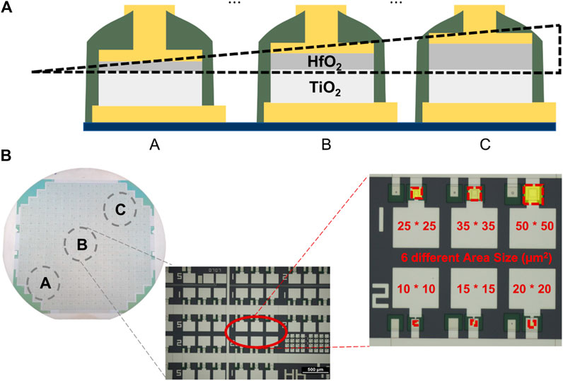
FIGURE 1. Schematic representation of the technology for bi-layer oxide memristive devices: Using different sputtering geometries (referred to as methods 1 and 2 in the text), different types of devices have been produced, showing filamentary switching (referred to as type F) and area-based resistance switching (referred to as type R). (A) Cross-section of TiN/TiOx/HfOx/Au bi-layer oxide memristive devices over the wafer. The used deposition method (method 2) allows for a variation of the thickness of HfOx layer from 2 to 8 nm. (B) Microscope images of a complete 4-inch wafer with 40,000 single devices and sections, showing the individual cells which consist of clusters with six devices, each with a different area size. Three regions on the wafer are indicated as A, B, and C. Each region has an area size of 0.5 × 0.5 cm2. For type R devices a 2 nm HfOx was deposited on all the three regions, while the thicknesses for type F have 2, 5, and 8 nm HfOx films on region A, B, and C, respectively. Here, it was assumed that the HfOx thickness is the same in each region due to the 1-dimensional thickness change over a 4-inch wafer and the relatively small area size. Approximately 60 memristive devices were measured in each area A, B, and C, respectively, for type F.
In more detail, the TiOx/HfOx bi-layer was deposited on an inertial reactive sputtered TiN bottom-electrode via DC magnetron sputtering, where O2/Ar of reactive gas was adjusted with the ratio of 10/40 and 10/29 for the TiOx and HfOx film, respectively. After the TiOx was sputtered, the thickness of the HfOx was controlled using the two discussed sputtering methods 1 (for device type R) and 2 (for device type F): as seen in Figure 1A a wedge layer with a variation of the HfOx thickness from 2 to 8 nm was obtained for device F, where devices were fabricated along the axis (x-direction) perpendicular to the axis of the wedge (y-direction). Device R has a 2 nm uniform HfOx layer. The layer deposition was finalized with an Au top-electrode layer. Thereafter, the material stack was patterned using photolithography and reactive ion etching for device R, while a lift-off in Dimethylsulfoxide (DMSO) was used for device F. The lift-off process was carried out due to the thickness variation of HfOx in device F. Here, the investigation of the switching behaviors was preceded after we confirmed that the two patterning methods scarcely affected electrical characteristics. All devices were insulated with SiO2 layers from the ambient air to avoid the influence of moisture in switching behaviors (Tsuruoka et al., 2012; Zhou et al., 2018; Zhou et al., 2020) (Figure 1A), and Al contact pads were deposited by e-beam evaporation.
2.2 Material Characterization
The development of the memristive devices was supported by a material characterization accompanying the manufacturing process. The thickness and the composition of the layers were characterized by ellipsometry measurements (SE500, Sentech) and surface profile measurements (Dektak 150, Veeco).
For a detailed material investigation, unstructured HfOx films were deposited on silicon substrates. Therefore, the two described sputtering methods 1 and 2 were employed to deposit 37 nm thick HfOx films. On those films ellipsometry measurements were performed at 632.8 nm at 70° of incidence. As the results, refractive indices of
Furthermore, X-ray photoelectron spectroscopy (XPS) measurement was utilized to study the quantitative atomic ratio O/Hf in sputtered HfOx layers. The XPS analysis were carried out using monochromatic Al_K-alpha radiation (excitation energy hν = 1,486.68 eV) under charge neutralization using a SPECS SAGE HR 150 XPS system equipped with a 1D delayline detector and a Phoibos 150 analyzer. The calibration of the energy scale was ensured by reference measurements on a polycrystalline silver sample. Before the measurements, HfOx was sputtered on Si/SiO2 wafers for 900 s using the two different sputtering method 1 and 2. As a result, a ratio of O/Hf of
2.3 Electrical Characterization
Current-voltage measurements (I-V curves) and voltage pulse measurements were carried out to characterize the electrical properties of TiOx/HfOx bi-layer memrsitive devices using a source measurement unit (Keysight b2901a). Therefore, a voltage is applied to the top-electrode of the device (bottom-electrode were grounded), while the current has been measured simultaneously. Furthermore, current compliance was imposed during the measurement to prevent the device from damage. The used current compliance was
2.4 Physics Based Device Model
For a profound understanding of the resistive switching mechanisms and a targeted development of the devices a physics based device model was developed. In Figure 2A a sketch of this device model is shown: the model consists of two RC elements representing, respectively, the HfOx and the TiOx layer. The metal-semiconductor contact between the HfOx layer and the Au electrode is considered by a Schottky diode (
An important difference between here investigated two types of memristive devices is sketched in Figure 2B. While for the type F device a filament of oxygen vacancies is formed under the external voltage application, the type R device does not form any filaments. Essential for this is the concentration of oxygen ions and vacancies in the active HfOx layer (Dirkmann et al., 2018). For the filamentary device F, we assumed that a number of oxygen vacancies are the mobile ions that vary between a minimum and a maximum concentration, denoted as
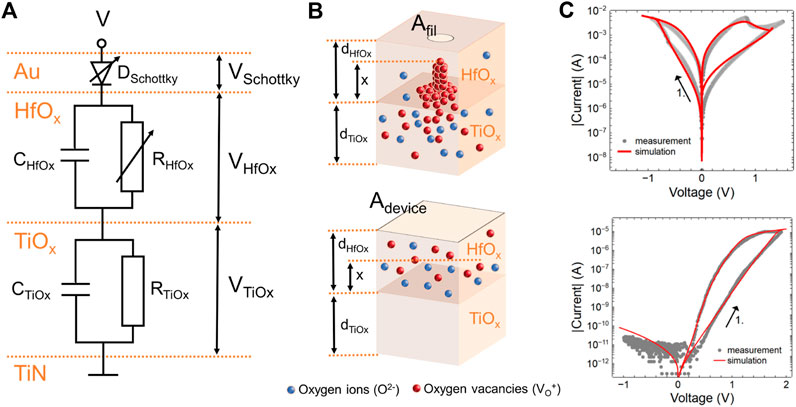
FIGURE 2. (A) Sketch of the physics based device model for TiN/TiOx/HfOx/Au memristive devices. The model consists of two RC elements in the TiOx and HfOx layers and a Schottky diode at the interface of HfOx and Au top-electrode. The external source voltage is divided into three local voltage drops at the HfOx, TiOx layers, and the Schottky diode. (B) Two different resistive switching mechanisms of type F devices (top) and type R devices (bottom) are considered. While in type F devices oxygen vacancies form a filamentary conductive path in the HfOx film under an external voltage, in type R devices oxygen ions in the HfOx film drift toward the top metal-electrode. As a result, in both device types the changed ion concentration leads to a modulation of the Schottky barrier height, which leads to the switching behaviors. Hereby originates the difference in the switching mechanisms from the density of the oxygen vacancies in the HfOx film. (C) Measured I-V curves (gray) and the simulation results (red) for type F (top) and type R (bottom) devices. The arrows point to the SET direction.
The concentration of the oxygen ions and vacancies has a particular effect on the active area used for resistance switching (cf. Figure 2B). Thus, for the filamentary device F only the filament area is relevant for the switching effect, i.e.,
where
The layer thickness of TiOx is significantly larger than that of HfOx. Therefore, a much lower local electrical field strength is assumed
where
where
The starting point of the switching model is the memristive behavior caused by a temporal and spatial change of the oxygen ions in the HfOx layer. This effect is taken into account in the device model via an average ion velocity.
where x is the memristive state variable, i.e., the average position of oxygen ions or length of the filament in the HfOx layer (cf. Figure 2B) and
Here,
An essential important property of ionic based memristive devices is the back diffusion of the ions. The back diffusion determines the reliability and the storage time of the memristive device and is crucial parameter for a precise adjustment of multiple resistance states. In order to consider this behavior in the model, a further term was added to Eq. 6:
Here
The ion current can be written in the following form using the law of Mott and Gurney (Hardtdegen et al., 2018):
where
The interface between the HfOx/Au is assumed to be the relevant interface for the resistive switching process in both types of devices. In the simulation, this interface is modeled as a Schottky diode with variable Schottky barrier (
Where n is the ideality factor, which describes the deviation from an ideal diode characteristic, and
where
Here
the values for
Here,
The device parameters have been carefully collected from measurements and literature and are summarized in Table 1. The I-V curves simulated with the model are shown in Figure 2C and compared with the measurement curves determined experimentally. As can be seen from this figure, the model presented here shows very good agreement with the experiment. A more detailed description of the results follows in the next chapter.
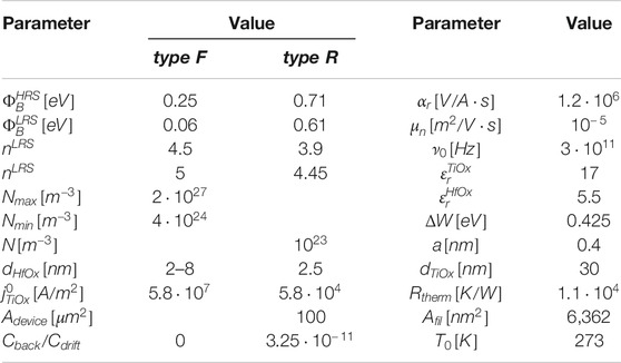
TABLE 1. Simulation Parameter.
3 Results and Discussion
3.1 Resistive Switching and Statistical Examinations
In Figure 3A typical obtained I-V curves of the two kinds of memristive devices (named as F and R) are shown. Common for both device types is that they show bipolar resistive switching with a gradual resistance change. A major difference between both types of devices is their voltage polarity. While type R devices require a positive voltage (applied to the top electrode) to set the device, type F devices require a negative voltage to be applied for the set process. The different polarity behaviors are originated from differences in concentration and species of mobile ions, which will be discussed in Concentration of Mobile Icon. Furthermore, while a highly rectifying memristive behavior is observed for device type R, a more symmetric memristive behavior is found for devices of type F together with a 3 times higher current level as compared to type R devices (cf. Figure 3A). In some more detail: the rectifying behavior of devices of type R can be quantified by the ratio between the maximum and minimum current
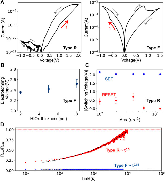
FIGURE 3. (A) Representative I-V curves of TiN/TiOx/HfOx/Au bi-layer memristive devices for type R (left), and type F (right). The arrows point to the resistive switching direction. A clear rectifying behavior was observed in the type R, and a symmetric switching behavior in the type F. (B) Electroforming voltage (median values) as a function of HfOx thickness. Electroforming voltages were tailored by the thickness of the HfOx in type F. (C) SET (blue) and RESET (red) voltages (median values) as a function of device active area size. The smaller the area is, the lower SET/RESET voltage was observed. (D) Retention measurement and fitting curves. Type F devices (blue) showed an improved retention characteristic compared to type R (red). The fitted curves are shown with dashed lines, and the fitting constants were 0.02 and 0.3 for type F and type R, respectively.
An important property of memristive devices and another difference between the here considered devices is the initial electroforming process. While no initial electroforming step was necessary for type R devices, type F devices had to be electroformed at the beginning. For a more precise discussion of the electroforming process of type F devices, the median of the required voltages as a function of the thickness of the HfOx layer is depicted in Figure 3B. In detail, electroforming voltages of 2.35, 2.42, and 2.52 V have been observed for, respectively, a 2, 5, and 8 nm thick HfOx layer. Thus, the electroforming voltage shows moderate thickness scalability. After the electroforming process type F device are operated typically at a maximum (minimum) voltage ±0.75 V. In terms of operating voltage, type F devices also differed from type R devices: type R devices require on average a 1.3 V higher operating voltage with a moderate area dependence (cf. Figure 3C). The operating voltages for type R devices were 2.2 V/−0.42 V (SET/RESET) for the smallest area size and 1.7V/0 V for the largest area size. However, the type R devices show a more gradual transition from the inertial high resistive state (HRS) to the low resistive state (LRS) (cf. Figure 3A).
A crucial property of memristive devices is their retention time. Furthermore, a detailed investigation of the retention characteristic already provides important conclusions about the underlying resistive switching mechanism (Hansen et al., 2015). The retention behavior for the here discussed two types of memristive bi-layer structures are shown in Figure 3D. For the measurement of the retention characteristics, the two types of devices were initially set to the low resistance state and then the resistance value of the devices was determined at regular intervals by means of voltage pulses. As can be seen in the figure, the two types of devices show quite different retention behaviors. For device type R, diffusive characteristics were observed (see red data points in Figure 3D), while much higher retention is observed for device type F. In order to analyze the retention characteristics in some more detail the retention curves were fitted using a power law according to the Curie-von Schweidler equation (Mikheev et al., 2014; Goossens et al., 2018):
where α is a fit parameter, which is between 0 and 1 (Yang et al., 2010). As a result, α = 0.3 is observed for devices of type R, whereas
In order to be able to make suitable statements about possible applications of the memristive devices in neuromorphic systems and to tailor the device characteristics accordingly, a statistical investigation of relevant device parameters is required. As relevant device parameters we considered the thickness of the active HfOx layer (
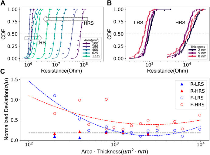
FIGURE 4. Resistance distribution for different physical device parameters in type R devices (A), and type F devices (B). (A) CDF for different active device area sizes of device type R. The arrows point to the direction of the increasing area. (B) CDF for different HfOx thicknesses in type F devices. (C) Device variability
To be able to make detailed statements about the requirements to be met by the physical device parameters, the influence of the variability in relation to the physical parameters must be examined. Therefore, normalized standard deviations of the devices were determined and plotted as a function of the active volume, i.e., the layer thickness of the active HfOx layer times the device area. The obtained results for both types of devices are shown in Figure 4C. The figure shows the different measured variabilities for the devices of type R (triangular data points) and the devices of type F (circular data points) as a function of the active volume of the device. For devices of type R it appears that the variability is only weakly affected by increased area size. Here the normalized standard deviation of 0.2 is quite constant over the investigated area sizes (see the dashed black line in Figure 4C). However, for devices of type F a parabolic curve best describes the found trend which indicates a clear optimum at approximately
3.2 Resistive Switching Mechanism and Device Requirements
A sound understanding of the resistive switching mechanism is important to enable a targeted design of the memristive devices for application in neuromorphic systems. For this reason, the device model described in Physics Based Device Model was used to interpret the experimental results described above. The obtained results are shown in Figure 2C. Therein the experimental I-V curves are compared with simulated curves. The used simulation parameters are summarized in Table 1. In both cases, i.e., in the case of the filamentary (type F device) and the interface-based device (type R device), one can see quite good agreement between simulation model and experiment. The main difference between the two I-V curves in the simulation model comes from (i) differences in concentration and species of mobile ions due to stoichiometric differences between Hf and O, (ii) different active areas that are responsible for the switching behavior (cf. Figure 2C), and (iii) the lowering of the Schottky barrier and the change of the ideality factor. In order to understand more exactly the underlying switching mechanisms that lead to the different device characteristics, the mentioned points (i–iii) will be discussed in the following in more detail.
3.2.1 Schottky Barrier Height Lowering
From the measured I-V curves the minimum and the maximum values of the variation of the Schottky barrier were determined. Therefore, Eq. 11 was adapted to the experimental data at the voltage interval ranging from 0 to 100 mV for both device types. Furthermore, we made the assumption that the resistance of the device does not change in that interval. As a result, we found that the values for the Schottky barriers vary between
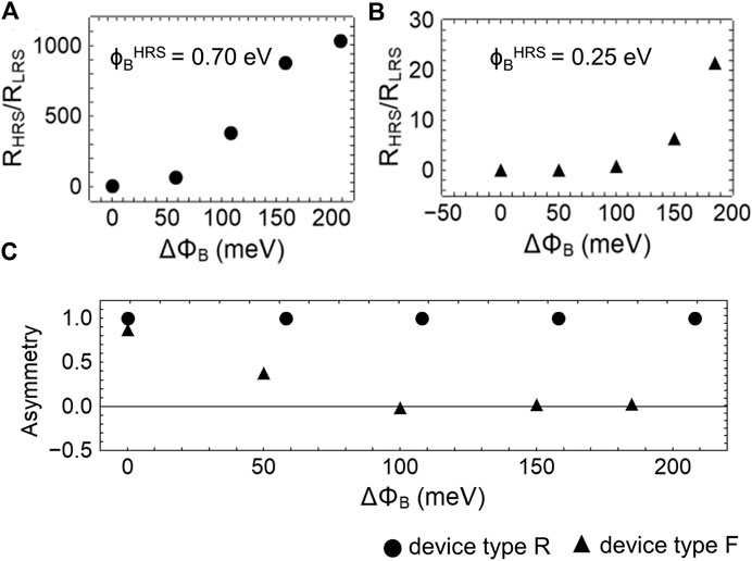
FIGURE 5. Influence of the Schottky barrier height lowering
In fact, a significant influence on the Schottky barrier height and therewith an important technology parameter is the material used for the electrode and the oxide layer. Since the same electrode material (Au) was used for both types of devices, the observed difference can only come from the HfOx layer. In this respect, the difference is mainly in the layer quality due to the different manufacturing processes that we used for the two devices. This has a particular effect on the number of oxygen ions and vacancies, which we will discuss in more detail below. However, a qualitative indicator of contact quality is the asymmetry between the minimum and the maximum current values in the I-V characteristics and the ideality factor n of the contacts. Here we observe that n is lower for the type R devices than for the type F devices and the type R devices show a clear asymmetry and therefore a stronger rectifying characteristic. To investigate this point, the asymmetry as a function of the barrier lowering
3.2.2 Concentration of Mobile Ions
One of the most important parameters for the resistance switching mechanism of memristive devices is the concentration of mobile ions. In the simulation model we have, therefore, investigated the concentration of mobile ions in the HfOx layer as a further central device parameter. It turned out that for the rectifying device R a constant low concentration of negatively charged oxygen ions (
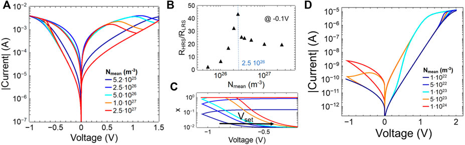
FIGURE 6. Simulated I-V curves of TiN/TiOx/HfOx/Au bi-layer memristive devices with a variation of the mean concentration of mobile ions in the HfOx layer. (A) The variation of the mean concentration of positively charged ions in the range from
Figure 6A shows I-V curves for the filamentary device with different mean concentrations of oxygen vacancies. In particular, two major trends for the change in oxygen vacancies can be seen: (i) the hysteresis shows a clear variation with the change of the oxygen vacancies, and (ii) the values for set and reset voltages become smaller. To interpret these two properties in more detail, Figure 6B shows the ratio
The results for the rectifying memristive device under varying concentrations of oxygen ions are shown in Figure 6D. Here it can be seen that the concentration of oxygen ions has an effect on the change of the resistance value as well as on the retention characteristics. Thus, at extremely low concentrations of oxygen ions, only small hysteric effects are observed, while a pronounced hysteresis is only observed at a concentration of
3.2.3 Area Dependence
An experimentally important indication of the type of resistive switching mechanism is given by the area dependence of the devices. For this purpose, the product of area times resistance (RA) as a function of the area of the devices is shown for both device types in Figure 7. While the upper graph of Figure 7 is presenting the results from the rectifying device R, the graph on the bottom is showing the area dependency for the filamentary device F. Here, the data points are taken from the measurements and the dashed lines are the results of the simulation model. The expected trend can be seen for the high resistant state of the devices: for the filamentary device F, an area independent behavior is seen, while a clear area dependence was found for the rectifying device R. It is noticeable that the low ohmic state of the rectifying device R shows a non-uniform area dependence. One would actually expect a horizontal line in the
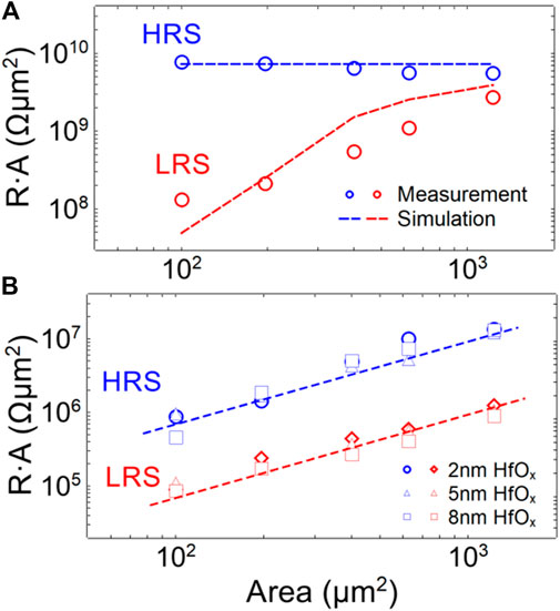
FIGURE 7. The
3.3 Applications for Neuromorphic Computing
The emulation of synaptic plasticity processes with memristive devices is one of the most important application fields of memristive devices in neuromorphic systems (Ziegler et al., 2018). In particular, this requires the design of suitable learning and training processes (Ielmini and Ambrogio, 2020), which needs a targeted adjustment of the resistance states of individual memristive devices in networks. In the following section, it is presented that type F devices fulfill requirements for machine learning based algorithms, whereas type R devices for neurobiologically inspired learning schemes.
The challenge in the machine learning based algorithm is to create suitable local learning rules that guarantee a local change of the device state so that a requested global network functionality is enabled. Therefore, a general framework is provided by the Hebbian learning rule (Ziegler et al., 2015), which can be systematized in the following equation:
where
where the coefficient α is named learning rate and is usually positive. Furthermore,
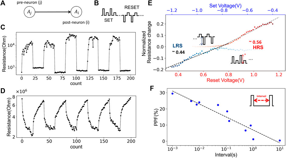
FIGURE 8. (A) Sketch of synaptic plasticity process. (B) The waveform of voltage pulse trains; 20 SET pulses followed by 20 RESET pulses. A readout pulse followed each switching pulse. The resulting change in resistance states under the voltage train is shown in (C) for type F, (D) for type R. The linearity in resistance change was improved in the type R. (E) The resistance as a function of the amplitude of SET/RESET voltages in type F. The amplitude of the applied voltage for a SET (RESET) was decreasing (increasing) to lead a next level in the resistance, and a readout voltage followed each switching voltage pulse. The multistate resistance was observed along with the symmetricity between LRS and HRS. (F) PPF as a function of interval time between two sequent switching voltage pulses in type R. The dashed line presents a fitted curve in the experimental data (blue). Increasing the time interval results in the weaker resistance change.
In order to investigate the resistance update behavior of the devices used here under voltage pulsing, AC pulses trains were used (see the sketch in Figure 8B). Therefore, a voltage train of 20 SET pulses followed by 20 RESET pulses was applied to the devices. Furthermore, the resistance states have been determined by a readout pulse that followed each switching pulse. The results obtained are shown in Figure 8C for type F devices and in (D) for type R devices. Read pulses of 1.0 and 0.1 V with a pulse width of 10 ms have been used for R and F devices, respectively. For the reset pulse, the width was 1 ms and the amplitudes were −2 and 1.5 V for R and F devices. As a result, a gradual transition change with multiple resistance states was observed in devices of type R, while a more binary behavior was recorded for devices of type F (cf. Figures 8C,D). In order to investigate the pulse behavior of the type F devices in more detail with respect to Eq. 18, the voltage amplitudes for SET and RESET pulses were successively changed in each pulse, as sketched in the inset of Figure 8E. The therewith obtained resistance change as a function of the voltage pulse amplitudes is shown in Figure 8E. Thus, a linear change in resistance with a successive incremental increase of the voltage pulse height was recorded for both set and reset. Furthermore, the resistance change was nearly symmetric in both resistance states, presenting 0.44 and 0.56 linearity for set and reset, respectively. Hence, this behavior fulfills nicely the requirement proposed by equation 18 and makes type F devices, together with their relatively good retention, perfect candidates for the hardware realization of deep learning neural networks. In this context, bi-layer oxide memristive devices of similar types have already proven their performance (Yao et al., 2020).
While the delta rule underlies a variety of machine learning systems and allows an effective implementation of Hebb’s learning rule within artificial neural networks, there is no explicit time dependence. However, the time dependence of learning processes is an important parameter in biology and determines how the synaptic connection is strengthened or weakened (Panwar et al., 2017). Here, an important property is the memory effect of synapses which leads to a sustained strengthening of the synaptic connection after repeated (high frequency) excitation named long-term potentiation (LTP). Therefore, the respective time interval between the excitation is required. At this respect, the diffusive ionic processes of memristive devices and their memory behavior are unique properties for the emulation of bio-realistic time-dependent learning (Ziegler et al., 2018), such as spike-timing dependent plasticity (STDP) and paired-pulse facilitation (PPF), to only mention two important plasticity processes. Many ways to emulate such learning schemes have been presented in recent years with memristive devices (Wang et al., 2020). However, the challenge here is to select the correct voltage functions for the pre- and post-neurons, so that an appropriate voltage pulse is applied across the memristive device (Linares-Barranco et al., 2011; Ambrogio et al., 2013). To investigate this for the type R device, we took a closer look at the PPF scheme. The results obtained,therefore, are shown in Figure 8F. Two identical sequential SET pulses were applied using different time intervals. In this study, the PPF ratio was defined as the incremental percentage change in the resistance after the first and second pulses. As a result, we found, the longer the time interval is, the smaller the resistance changes with a linear trend. This, particularly, corresponds to the enhanced back diffusion of oxygen ions in R type devices, as discussed above, and resembles well with biology.
4 Conclusion
In summary, we have presented two bi-layer TiN/TiOx/HfOx/Au memristive devices. Depending on the respective sputtering method, we were able to realize different switching mechanisms. While mobile oxygen ions are responsible for resistance switching in type R devices, oxygen vacancies cause the switching mechanism in type F devices. Using a statistical analysis of the devices and a physical device model, we have investigated the relevant technology and device parameters, and related them to the electronic behavior of the devices. In Figure 9 these parameters are graphically summarized and their relevance for the respective device type is shown. As you can see from that figure for devices of type R, whose resistive switching is induced by mobile oxygen ions, the device area (
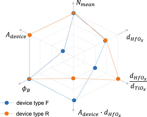
FIGURE 9. Relevant technology and device parameters to realize a desired resistive switching behavior in the TiN/TiOx/HfOx/Au bi-layer memristive devices.
Data Availability Statement
The original contributions presented in the study are included in the article/Supplementary Material, further inquiries can be directed to the corresponding authors.
Author Contributions
SP prepared the samples, JD developed the sputtering technology for the HfOx films, and the characteristics of HfOx films were analyzed using XPS by AK. SP performed the measurements, analyzed the experimental results, and co-wrote the manuscript. SK supervised the electronic measurement. MZ supported the measurements and data interpretation. MZ developed the simulation model. The simulation results were discussed and interpreted between SP, TI, SK, and MZ. TI and MZ conceived the idea, initiated, and supervised the experimental research. SP and MZ discussed the experimental results and contributed to the refinement of the manuscript.
Funding
Funded by the Deutsche Forschungsgemeinschaft (DFG, German Research Foundation)–Project-ID 434434223–SFB 1461 and the Carl-Zeiss Foundation via the Project MemWerk.
Conflict of Interest
The authors declare that the research was conducted in the absence of any commercial or financial relationships that could be construed as a potential conflict of interest.
Supplementary Material
The Supplementary Material for this article can be found online at: https://www.frontiersin.org/articles/10.3389/fnano.2021.670762/full#supplementary-material.
References
Alibart, F., Zamanidoost, E., and Strukov, D. B. (2013). Pattern Classification by Memristive Crossbar Circuits Using ex situ and in situ Training. Nat. Commun. 4, 1–7. doi:10.1038/ncomms3072
Ambrogio, S., Balatti, S., Nardi, F., Facchinetti, S., and Ielmini, D. (2013). Spike-Timing Dependent Plasticity in a Transistor-Selected Resistive Switching Memory. Nanotechnology 24, 384012. doi:10.1088/0957-4484/24/38/384012
Asanuma, S., Akoh, H., Yamada, H., and Sawa, A. (2009). Relationship Between Resistive Switching Characteristics and Band Diagrams of Ti/Pr1−xCaxMnO3Junctions. Phys. Rev. B. 80, 235113. doi:10.1103/PhysRevB.80.235113
Bousoulas, P., Asenov, P., Karageorgiou, I., Sakellaropoulos, D., Stathopoulos, S., and Tsoukalas, D. (2016). Engineering Amorphous-Crystalline Interfaces in tio2-x/tio2-y-Based Bilayer Structures for Enhanced Resistive Switching and Synaptic Properties. J. Appl. Phy. 120, 154501. doi:10.1063/1.4964872
Chandrasekaran, S., Simanjuntak, F. M., Saminathan, R., Panda, D., and Tseng, T. Y. (2019). Improving Linearity by Introducing Al in hfo2 as a Memristor Synapse Device. Nanotechnology 30, 445205. doi:10.1088/1361-6528/ab3480
Clima, S., Chen, Y. Y., Chen, C. Y., Goux, L., Govoreanu, B., Degraeve, R., et al. (2016). First-Principles Thermodynamics and Defect Kinetics Guidelines for Engineering a Tailored RRAM Device. J. Appl. Phy. 119, 225107. doi:10.1063/1.4953673
Cüppers, F., Menzel, S., Bengel, C., Hardtdegen, A., von Witzleben, M., Böttger, U., et al. (2019). Exploiting the Switching Dynamics of hfo2-Based Reram Devices for Reliable Analog Memristive Behavior. APL Mater. 7, 091105. doi:10.1063/1.5108654
del Valle, J., Ramírez, J. G., Rozenberg, M. J., and Schuller, I. K. (2018). Challenges in Materials and Devices for Resistive-Switching-Based Neuromorphic Computing. J. Appl. Phy. 124, 211101. doi:10.1063/1.5047800
Diederich, N., Bartsch, T., Kohlstedt, H., and Ziegler, M. (2018). A Memristive Plasticity Model of Voltage-Based stdp Suitable for Recurrent Bidirectional Neural Networks in the Hippocampus. Sci. Rep. 8, 1–12. doi:10.1038/s41598-018-27616-6
Dirkmann, S., Hansen, M., Ziegler, M., Kohlstedt, H., and Mussenbrock, T. (2016). The Role of ion Transport Phenomena in Memristive Double Barrier Devices. Sci. Rep. 6. 35686. doi:10.1038/srep1375310.1038/srep35686
Dirkmann, S., Kaiser, J., Wenger, C., and Mussenbrock, T. (2018). Filament Growth and Resistive Switching in Hafnium Oxide Memristive Devices. ACS Appl. Mater. Inter. 10, 14857–14868. doi:10.1021/acsami.7b19836
Dittmann, R., and Strachan, J. P. (2019). Redox-Based Memristive Devices for new Computing Paradigm. APL Mater. 7, 110903. doi:10.1063/1.5129101
Gao, J., He, G., Deng, B., Xiao, D. Q., Liu, M., Jin, P., et al. (2016). Microstructure, Wettability, Optical and Electrical Properties of hfo2 Thin Films: Effect of Oxygen Partial Pressure. J. Alloy. Compd. 662, 339–347. doi:10.1016/j.jallcom.2015.12.080
Gao, S., Zeng, F., Li, F., Wang, M., Mao, H., Wang, G., et al. (2015). Forming-Free and Self-Rectifying Resistive Switching of the Simple pt/tao x/N-Si Structure for Access Device-Free High-Density Memory Application. Nanoscale 7, 6031–6038. doi:10.1039/c4nr06406b
Goossens, A. S., Das, A., and Banerjee, T. (2018). Electric Field Driven Memristive Behavior at the Schottky Interface of Nb-Doped srtio3. J. Appl. Phy. 124, 152102. doi:10.1063/1.5037965
Govoreanu, B., Redolfi, A., Zhang, L., Adelmann, C., Popovici, M., Clima, S., et al. (2013). “Vacancy-Modulated Conductive Oxide Resistive Ram: an Area-Scalable Switching Current, Self-Compliant, Highly Nonlinear and Wide on/off-Window Resistive Switching Cell,” in IEEE International Electron Devices Meeting, Washington, DC, December 9–11, 2013 (New York, NY: IEEE), 10–12.
Hansen, M., Zahari, F., Kohlstedt, H., and Ziegler, M. (2018). Unsupervised Hebbian Learning Experimentally Realized With Analogue Memristive Crossbar Arrays. Sci. Rep. 8, 1–10. doi:10.1038/s41598-018-27033-9
Hansen, M., Zahari, F., Ziegler, M., and Kohlstedt, H. (2017). Double-Barrier Memristive Devices for Unsupervised Learning and Pattern Recognition. Front. Neurosci. 11, 91. doi:10.3389/fnins.2017.00091
Hansen, M., Ziegler, M., and Kolberg, L. (2015). A Double Barrier Memristive Device. Sci. Rep. 5, 13753. doi:10.1038/srep13753
Hardtdegen, A., Torre, C. L., Cüppers, F., Menzel, S., Waser, R., and Hoffmann-Eifert, S. (2018). Improved Switching Stability and the Effect of an Internal Series Resistor in hfo2/tiox Bilayer Reram Cells. IEEE Trans. Electron Devices 65, 3229–3236. doi:10.1109/TED.2018.2849872
He, W., Sun, H., Zhou, Y., Lu, K., Xue, K., and Miao, X. (2017). Customized Binary and Multi-Level HfO2−x-Based Memristors Tuned by Oxidation Conditions. Sci. Rep. 7, 10070. doi:10.1038/s41598-017-09413-9
Huang, C. H., Huang, J. S., Lin, S. M., Chang, W. Y., He, J. H., and Chueh, Y. L. (2012). Zno1–x Nanorod arrays/zno Thin Film Bilayer Structure: From Homojunction Diode and High-Performance Memristor to Complementary 1d1r Application. Acs Nano 6, 8407–8414. doi:10.1021/nn303233r
Hur, J. H., Lee, M.-J., Lee, C. B., Kim, Y.-B., and Kim, C.-J. (2010). Modeling for Bipolar Resistive Memory Switching in Transition-Metal Oxides. Phys. Rev. B 82, 155321. doi:10.1103/PhysRevB.82.155321
Ielmini, D., and Ambrogio, S. (2020). Emerging Neuromorphic Devices. Nanotechnology 31, 092001. doi:10.1088/1361-6528/ab554b
Ielmini, D., and Milo, V. (2017). Physics-Based Modeling Approaches of Resistive Switching Devices for Memory and in-Memory Computing Applications. J. Comput. Electron 16, 1121–1143. doi:10.1007/s10825-017-1101-9
Ignatov, M., Ziegler, M., Hansen, M., and Kohlstedt, H. (2017). Memristive Stochastic Plasticity Enables Mimicking of Neural Synchrony: Memristive Circuit Emulates an Optical Illusion. Sci. Adv. 3, e1700849. doi:10.1126/sciadv.1700849
Jeong, H., and Shi, L. (2019). Memristor Devices for Neural Networks. J. Phys. D 52, 023003. doi:10.1088/1361-6463/aae223
Jiang, Z., Wu, Y., Yu, S., Yang, L., Song, K., Karim, Z., et al. (2016). A Compact Model for Metal–Oxide Resistive Random Access Memory With Experiment Verification. IEEE Trans. Electron Devices 63, 1884–1892. doi:10.1109/ted.2016.2545412
Kendall, J. D., Pantone, R. D., and Nino, J. C. (2020). Data From: Deep Learning in Memristive Nanowire Networks. http://arXiv:2003.02642.
Kim, H. J., Zheng, H., Park, J. S., Kim, D. H., Kang, C. J., Jang, J. T., et al. (2017). Artificial Synaptic Characteristics With Strong Analog Memristive Switching in a pt-ceo2-pt Structure. Nanotechnology 28, 285203. doi:10.1088/1361-6528/aa712c
Kim, S. G., Han, J. S., Kim, H., Kim, S. Y., and Jang, H. W. (2018). Recent Advances in Memristive Materials for Artificial Synapses. Adv. Mater. Technol. 3, 1800457. doi:10.1002/admt.201800457
Krestinskaya, O., James, A. P., and Chua, L. O. (2020). Neuromemristive Circuits for Edge Computing: a Review. IEEE Trans. Neural Netw. Learn. Syst. 31, 4–23. doi:10.1109/TNNLS.2019.2899262
Lee, J., Shin, J., Lee, D., Lee, W., Jung, S., Jo, M., et al. (2010). “Diode-Less Nano-Scale zro x/hfo x rram Device With Excellent Switching Uniformity and Reliability for High-Density Cross-Point Memory Applications,” in International Electron Devices Meeting. San Francisco, CA. December 6–8, 2010 (New York, NY: IEEE), 19–25.
Lee, J., Park, J., Jung, S., and Hwang, H. (2011). “Scaling Effect of Device Area and Film Thickness on Electrical and Reliability Characteristics of rram,” in International Interconnect Technology Conference. Dresden, Germany. May 8–12 , 2011 (New York, NY: IEEE), 1–3.
Legenstein, R. (2015). Nanoscale Connections for Brain-Like Circuits. Nature 521, 37–38. doi:10.1038/521037a
Li, J., Zhang, T., Duan, Q., Li, L., Yang, Y., and Huang, R. (2018a). “Engineering Resistive Switching Behavior in Taox Based Memristive Devices for non-von Neuman Computing Applications,” in China Semiconductor Technology International Conference. Shanghai, China. March 11–12, 2018 (New York, NY: IEEE), 1–3.
Li, Y., Wang, Z., Midya, R., Xia, Q., and Yang, J. J. (2018b). Review of Memristor Devices in Neuromorphic Computing: Materials Sciences and Device Challenges. J. Phys. D 51, 503002. doi:10.1088/1361-6463/aade3f
Li, Y., Fuller, E. J., Sugar, J. D., Yoo, S., Ashby, D. S., Bennett, C. H., et al. (2020). Filament‐Free Bulk Resistive Memory Enables Deterministic Analogue Switching. Adv. Mater. 32, 2003984. doi:10.1002/adma.202003984
Lin, P., Li, C., Wang, Z., Li, Y., Jiang, H., Song, W., et al. (2020). Three-dimensional Memristor Circuits as Complex Neural Networks. Nat. Electron. 3, 225–232. doi:10.1038/s41928-020-0397-9
Linares-Barranco, B., Serrano-Gotarredona, T., Camuñas-Mesa, L. A., Perez-Carrasco, J. A., Zamarreño-Ramos, C., and Masquelier, T. (2011). On Spike-Timing-Dependent-Plasticity, Memristive Devices, and Building A Self-Learning Visual Cortex. Front. Neurosci. 5, 26. doi:10.3389/fnins.2011.00026
Ma, H., Feng, J., Lv, H., Gao, T., Xu, X., Luo, Q., et al. (2017). Self-Rectifying Resistive Switching Memory with Ultralow Switching Current in Pt/Ta2O5/HfO2-x/Hf Stack. Nanoscale Res. Lett. 12, 1–6. doi:10.1186/s11671-017-1905-3
Martínez, F. L., Toledano-Luque, M., Gandía, J. J., Cárabe, J., Bohne, W., Röhrich, J., et al. (2007). Optical Properties and Structure of hfo2thin Films Grown by High Pressure Reactive Sputtering. J. Phys. D 40, 5256. doi:10.1088/0022-3727/40/17/037
Massimiliano, B., and Yuriy, P. (2013). On the Physical Properties of Memristive, Memcapacitive and Meminductive Systems. Nanotechnology 24, 7. doi:10.1088/0957-4484/24/25/255201
McKenna, K. P. (2014). Optimal Stoichiometry for Nucleation and Growth of Conductive Filaments in hfox. Model. Simul. Mater. Sci. Eng. 22, 025001. doi:10.1088/0965-0393/22/2/025001
Menzel, S., Waters, M., Marchewka, A., Böttger, U., Dittmann, R., and Waser, R. (2011). Origin of the Ultra-Nonlinear Switching Kinetics in Oxide-Based Resistive Switches. Adv. Funct. Mater. 21, 4487–4492. doi:10.1002/adfm.201101117
Mikhaylov, A., Belov, A., Korolev, D., Antonov, I., Kotomina, V., Kotina, A., et al. (2020). Multilayer Metal-Oxide Memristive Device with Stabilized Resistive Switching. Adv. Mater. Technol. 5, 1900607. doi:10.1002/admt.201900607
Mikheev, E., Hoskins, B. D., and Strukov, D. B. (2014). Resistive Switching and its Suppression in pt/nb:srtio3 Junctions. Nat. Commun. 5, 3990. doi:10.1038/ncomms4990
Mohammad, B., Jaoude, M. A., Kumar, V., Al Homouz, D. M., Nahla, H. A., Al-Qutayri, M., et al. (2016). State of the art of Metal Oxide Memristor Devices. Nanotechno. Rev. 5, 311–329. doi:10.1515/ntrev-2015-0029
Niu, D., Chen, Y., Xu, C., and Xie, Y. (2010). “Impact of Process Variations on Emerging Memristor”. in Proceedings of the 47th Design Automation Conference. San Francisco, CA. July 13–18, 2010 (DAS), (New York, NY: IEEE) 877–882.
Panwar, N., Rajendran, B., and Ganguly, U. (2017). Arbitrary Spike Time Dependent Plasticity in Memristor by Analog Waveform Engineering. IEEE Electron Device Lett. 38, 740–743. doi:10.1109/LED.2017.2696023
Park, T. H., Song, S. J., Kim, H. J., Kim, S. G., Chung, S., Kim, B. Y., et al. (2015). Thickness Effect of Ultra-Thin Ta 2 O 5 Resistance Switching Layer in 28 nm-Diameter Memory Cell. Sci. Rep. 5, 15965. doi:10.1038/srep15965
Payvand, M., Muller, L. K., and Indiveri, G. (2018). “Event-Based Circuits for Controlling Stochastic Learning with Memristive Devices in Neuromorphic Architectures,” in International Symposium on Circuits and Systems. Florence, Italy. May 27–30, 2018 (New York, NY: IEEE), 1–5.
Pei, J.-S., Wright, J. P., Todd, M. D., Masri, S. F., and Gay-Balmaz, F. (2015). Understanding Memristors and Memcapacitors in Engineering Mechanics Applications. Nonlinear Dyn. 80, 457–489. doi:10.1007/s11071-014-1882-3
Prezioso, M., Merrikh-Bayat, F., Hoskins, B. D., Adam, G. C., Likharev, K. K., and Strukov, D. B. (2015). Training and Operation of an Integrated Neuromorphic Network Based on Metal-Oxide Memristors. Nature 521, 61–64. doi:10.1038/nature14441
Sah, M. P., Kim, H., and Chua, L. (2014). Brains are Made of Memristors. IEEE Circuits Syst. Mag. 14, 12–36. doi:10.1109/MCAS.2013.2296414
Snider, G. S. (2008). “Spike-Timing-Dependent Learning in Memristive Nanodevices,” in International Symposium on Nanoscale Architectures. Anaheim, CA. June 12–13, 2008 (New York, NY: IEEE), 85–92.
Solan, E., Dirkmann, S., Hansen, M., Schroeder, D., Kohlstedt, H., Ziegler, M., et al. (2017). An Enhanced Lumped Element Electrical Model of a Double Barrier Memristive Device. J. Phys. D 50, 195102. doi:10.1088/1361-6463/aa69ae
Stathopoulos, S., Khiat, A., Trapatseli, M., Cortese, S., Serb, A., Valov, I., et al. (2017). Multibit Memory Operation of Metal-Oxide Bi-Layer Memristors. Sci. Rep. 7, 17532. doi:10.1038/s41598-017-17785-1
Sun, W., Gao, B., Chi, M., Xia, Q., Yang, J. J., Qian, H., et al. (2019). Understanding Memristive Switching via in Situ Characterization and Device Modeling. Nat. Commun. 10, 1–13. doi:10.1038/s41467-019-11411-6
Sze, S., and Ng, K. K. (2006). Physics of Semiconductor Devices. Hoboken, New Jersey: John Wiley & Sons, Ltd.
Tsuruoka, T., Terabe, K., Hasegawa, T., Valov, I., Waser, R., and Aono, M. (2012). Effects of Moisture on the Switching Characteristics of Oxide-Based, Gapless-Type Atomic Switches. Adv. Funct. Mater. 22 70–77. doi:10.1002/adfm.201101846
Versace, M., and Chandler, B. (2010). The Brain of a new Machine. IEEE Spectr. 47, 30–37. doi:10.1109/MSPEC.2010.5644776
Wang, C., Xiong, L., Sun, J., and Yao, W. (2019). Memristor-Based Neural Networks With Weight Simultaneous Perturbation Training. Nonlinear Dyn. 95, 2893–2906. doi:10.1007/s11071-018-4730-z
Wang, M., Luo, W. J., Wang, Y. L., Yang, L. M., Zhu, W., Zhou, P., et al. (2010). “A Novel Cuxsiyo Resistive Memory in Logic Technology with Excellent Data Retention and Resistance Distribution for Embedded Applications,” in Symposium on VLSI Technology. Honolulu, HI. June 15–17, 2010 (New York, NY: IEEE), 89–90.
Wang, R., Yang, J.-Q., Mao, J.-Y., Wang, Z.-P., Wu, S., Zhou, M., et al. (2020). Recent Advances of Volatile Memristors: Devices, Mechanisms, and Applications. Adv. Intell. Sys. 2, 2000055. doi:10.1002/aisy.202000055
Wang, Y.-F., Lin, Y.-C., Wang, I.-T., Lin, T.-P., and Hou, T.-H. (2015). Characterization and Modeling of Nonfilamentary Ta/TaOx/TiO2/Ti Analog Synaptic Device. Sci. Rep. 5, 10150. doi:10.1038/srep10150
Wang, Z., Yin, M., Zhang, T., Cai, Y., Wang, Y., Yang, Y., et al. (2016). Engineering Incremental Resistive Switching in Taoxbased Memristors for Brain-Inspired Computing. Nanoscale 8, 14015–14022. doi:10.1039/C6NR00476H
Xiong, W., Zhu, L. Q., Ye, C., Yu, F., Ren, Z. Y., and Ge, Z. Y. (2019). Bilayered Oxide‐Based Cognitive Memristor with Brain‐Inspired Learning Activities. Adv. Electron. Mater. 5, 1900439. doi:10.1002/aelm.20190043
Yakopcic, C., Hasan, R., and Taha, T. M. (2015). “Memristor Based Neuromorphic Circuit for ex-situ Training of Multi-Layer Neural Network Algorithms,” in International Joint Conference on Neural Networks. July 12–17, 2015 (New York, NY: IEEE), 1–7.
Yang, C.-H., Kuo, Y., and Lin, C.-H. (2010). Charge Detrapping and Dielectric Breakdown of Nanocrystalline Zinc Oxide Embedded Zirconium-Doped Hafnium Oxide High-K Dielectrics for Nonvolatile Memories. Appl. Phys. Lett. 96, 192106. doi:10.1063/1.3429590
Yao, P., Huaqiang, W., Wu, H., Tang, J., Zhang, Q., Zhang, W., et al. (2020). Fully Hardware-Implemented Memristor Convolutional Neural Network. Nature 577, 641–646. doi:10.1038/s41586-020-1942-4
Yin, X.-B., Tan, Z.-H., and Guo, X. (2015). The Role of Schottky Barrier in the Resistive Switching of SrTiO3: Direct Experimental Evidence. Phys. Chem. Chem. Phys. 17, 134–137. doi:10.1039/c4cp04151h
Yoon, J. H., Song, S. J., Yoo, I.-H., Seok, J. Y., Yoon, K. J., Kwon, D. E., et al. (2014). Highly Uniform, Electroforming-Free, and Self-Rectifying Resistive Memory in the pt/ta2o5/hfo2-x/tin Structure. Adv. Funct. Mater. 24, 5086–5095. doi:10.1002/adfm.201400064
Zhao, M., Gao, B., Tang, J., Qian, H., and Wu, H. (2020). Reliability of Analog Resistive Switching Memory for Neuromorphic Computing. Appl. Phy. Rev. 7, 011301. doi:10.1063/1.5124915
Zhou, G., Duan, S., Li, P., Sun, B., Wu, B., Yao, Y., et al. (2018). Coexistence of Negative Differential Resistance and Resistive Switching Memory at Room Temperature in Tio x Modulated by Moisture. Adv. Electron. Mater. 4, 1700567. doi:10.1002/aelm.201700567
Zhou, G., Ren, Z., Sun, B., Wu, J., Zou, Z., Zheng, S., et al. (2020). Capacitive Effect: an Original of the Resistive Switching Memory. Nano Energy 68, 104386. doi:10.1016/j.nanoen.2019.104386
Zhou, G., Sun, B., Yao, Y., Zhang, H., Zhou, A., Alameh, K., et al. (2016). Investigation of the Behaviour of Electronic Resistive Switching Memory Based on Mose2-Doped Ultralong se Microwires. Appl. Phys. Lett. 109, 143904. doi:10.1063/1.4962655
Ziegler, M., Riggert, C., Hansen, M., Bartsch, T., and Kohlstedt, H. (2015). Memristive Hebbian Plasticity Model: Device Requirements for the Emulation of Hebbian Plasticity Based on Memristive Devices. IEEE Trans. Biomed. Circuits Syst. 9, 197–206. doi:10.1109/tbcas.2015.2410811
Keywords: memristive devices, neuromorphic systems, bi-layer oxide memristive devices, memristive layer engineering, numerical simulation
Citation: Park S, Klett S, Ivanov T, Knauer A, Doell J and Ziegler M (2021) Engineering Method for Tailoring Electrical Characteristics in TiN/TiOx/HfOx/Au Bi-Layer Oxide Memristive Devices. Front. Nanotechnol. 3:670762. doi: 10.3389/fnano.2021.670762
Received: 22 February 2021; Accepted: 26 March 2021;
Published: 27 April 2021.
Edited by:
Huanglong Li, Tsinghua University, ChinaReviewed by:
Guangdong Zhou, Southwest University, ChinaDashan Shang, Institute of Microelectronics, China
Copyright © 2021 Park, Klett, Ivanov, Knauer, Doell and Ziegler. This is an open-access article distributed under the terms of the Creative Commons Attribution License (CC BY). The use, distribution or reproduction in other forums is permitted, provided the original author(s) and the copyright owner(s) are credited and that the original publication in this journal is cited, in accordance with accepted academic practice. No use, distribution or reproduction is permitted which does not comply with these terms.
*Correspondence: Seongae Park, c2VvbmdhZS5wYXJrQHR1LWlsbWVuYXUuZGU=; Martin Ziegler, bWFydGluLnppZWdsZXJAdHUtaWxtZW5hdS5kZQ==