 Susmita Bhattacharya
 Goutam Kumar Chandra2*
- 1Department of Physics, RGUKT Nuzvid, Nuzvid, India
- 2Department of Physics, NIT Calicut, Kozhikode, India
Recent observations have demonstrated that the photoelectric conversion properties of perovskite materials are intimately related to the presence of superlattice structures and other unusual nanoscale features in them. The low-dimensional or mixed-dimensional halide perovskite families are found to be more efficient materials for device application than three-dimensional halide perovskites. The emergence of perovskite solar cells has revolutionized the solar cell industry because of their flexible architecture and rapidly increased efficiency. Tuning the dielectric constant and charge separation are the main objectives in designing a photovoltaic device that can be explored using the two-dimensional perovskite family. Thus, revisiting the fundamental properties of perovskite crystals could reveal further possibilities for recognizing these improvements toward device functionality. In this context, this review discusses the material properties of two-dimensional halide perovskites and related optoelectronic devices, aiming particularly for solar cell applications.
Introduction
As witnessed in the past decade, the halide perovskite (HP) family has emerged as a high-performance photovoltaic (PV) material. This reappearance has involved extensive development of the three-dimensional (3D) perovskites, specifically CH3NH3PbI3. The crystallographic formula ABX3 of HP materials comprised A, an organic cation such as methylammonium (MA): CH3NH2+ or an alkali cation or mixing of both, B, the metal cation (Pb+2 or Sn+2), and X, the halide anions (X = I−, Br−, or Cl−). HPs are mainly classified into two categories depending on whether an organic-molecular cation or an elemental cation is occupying the A-site. These categories are organic–inorganic hybrid HPs and all-inorganic HPs, respectively. In hybrid HPs, the organic cations occupying the A-site of the perovskite structure are usually nonsymmetric and inclined to rotation at room temperature and above (Chen et al., 2015). This extraordinary phenomenon has hardly been observed in other materials. As a result, hybrid HPs have the interconnected [BX6]4 octahedra continuing in an ordered manner that forms the crystal structure with the local disorder located within the [BX6]4 framework. At room temperature, in the most-reviewed hybrid HP, CH3NH3PbI3 or (MAPbI3), the reorientation of the polar MA+ ion is found in [PbI6]4 octahedral structures (between the faces, corners, or edges) having a residence time of ∼14 ps (Leguy et al., 2015). At lower temperatures, the rotational dynamics in HPs are slowed down (Wu et al., 2017) following their dielectric response. HPs can have different tunable chemical compositions, such as A2BX4, ABX4, and A3BX9, well known as Ruddlesden–Popper (RP) phases (Yu et al., 2017). The defects in the crystal, crystallographic alignments, surfaces, grain boundaries, and interfaces in HPs can be customized preferentially. These preferential nano- and microstructures can be addressed using in-depth conventional microscopic characterization methods such as atomic force microscopy (AFM), scanning electron microscopy (SEM), and transmission electron microscopy (TEM). As an example, consider the case of a perovskite solar cell (PSC). A PSC includes a hybrid organic–inorganic or all-inorganic perovskite-structured compound as the light-harvesting active layer. The compositional variation of the material and its dependency on the phase transition temperature are related to the electrical and ionic properties of the active layer (Lee et al., 2012; Correa-Baena et al., 2017; Zhou et al., 2019). Thus, we can infer that measuring a minute variation of structural property and optimizing the same will be a quality control measure for optoelectronic devices.
The large exciton binding energy due to the reduced dielectric screening and quantum confinement is the most fascinating optoelectronic property of two-dimensional (2D) materials. 2D HPs with their tunable photophysical properties and superior chemical stability compared to their 3D counterpart (Ding et al., 2018; Zheng et al., 2018, Dong et al., 2019) have created a great influence on the semiconductor research and technology fields. 2D HPs obey stereochemical rules that determine the growth of the perovskite sheets, and (a) corner-sharing, (b) edge-sharing, and (c) face-sharing octahedral connections have been experimentally observed. Here, the characteristics for size restriction for the A-site are determined by the suitability of a cation spacer with respect to (a) its net +ve charge at the perovskite-attaching point and substitution amount, (b) capacity of hydrogen bonding, (c) flexible stereochemical arrangement, and (d) ability of space filling (Mao et al., 2019). Most cations are found to have a corner-sharing 2D structure, but sometimes the cation-imposed configuration strain in the 2D network stabilizes edge-sharing or face-sharing networks (Kamminga et al., 2016). In 2D perovskites, extra larger organic cations (L) are inserted as spacers, separating the inorganic metal halide octahedra layers to form quantum well (QW) superlattices that are different from those of conventional 3D HPs. Here, introducing hydrophobic spacer cations, the ionic lattice of inorganic octahedrons is effectively isolated from the ambient water molecules. The newly introduced additional spacing cations and asymmetric lattice structures provide tunable intrinsic physical features, such as dielectric constant, optical bandgap, and exciton binding energy (Blancon et al., 2017). As a result, the photophysical behaviors like exciton dynamics (Proppe et al., 2019), charge carrier transport (Tsai et al., 2018), and electron−phonon coupling (Straus and Kagan, 2018) that strongly influence the performance of optoelectronic devices [light emitting diode (LED), solar cell (SC), etc.] can also be modulated accordingly (Zheng et al., 2018). In a recent report, the mechanical properties of (C6H5CH2NH3)2PbCl4 were found to be anisotropic, and where the organic components and van der Waals interactions between layers play a significant role in the 2D structural stability (Gao et al., 2020). They found that substituting the organic parts with rigid and multifunctional organic components with Pb improved the stability and carrier mobility of the PSC absorber layer.
The interaction of electromagnetic fields with photo- and electro-active materials is the heart of energy conversion research. Graphene, hexagonal boron nitride (BN), transition metal dichalcogenides (TMDs), MXenes, and other classical 2D materials are being widely studied due to their fascinating properties such as high electrical conductivity, low density, large surface area, and tunable electric and magnetic properties (Novoselov et al., 2004; Mas-Ballesté et al., 2011; Jiang et al., 2020). Pristine graphene is a zero-bandgap semimetal, while graphene oxide (GO) and reduced graphene oxide (RGO) are an insulator and a semiconductor, respectively. 2D TMDs display a semiconducting nature (Rao et al., 2009; Ferrari et al., 2015). MXenes sometimes behave as metals, semiconductors, superconductors, topological insulators, and, most importantly, half-metals (Naguib et al., 2011; Naguib et al., 2012; Anasori et al., 2015). Graphene and related 2D materials propose an extraordinary advancement toward device performance even at the atomic scale. A compromised combination of these 2D materials with silicon chips promotes a massively enhanced potential compatibility on silicon technology. Low-cost, simple, and inexpensive layered 2D HPs are a novel class of materials with outstanding layer-dependent tunable optical properties that generates room temperature stable excitons and modified exciton binding energy due to quantum and dielectric confinement effects. Layered 2D HPs also offer the improved environmental stability and photostability needed for the light-absorbing layer of photovoltaic devices. The recent progress in the field of 2D HPs and the respective SC technology has been illustrated in Figure 1. This review describes the enormous potential of this thin film SC technology, expected to become a low-cost commercial alternative to the presently available silicon photovoltaic devices in the near future. The manuscript evolves as follows: introduction to material properties, followed by highlighting 2D perovskite structural aspects, while in the next section, the material characterization that identifies the exotic material property of 2D HPs has been discussed. Finally, the microstructural characteristics of 2D HPs that lead to promising potential applications as high-performance optoelectronic devices, especially SCs, have been pointed out.
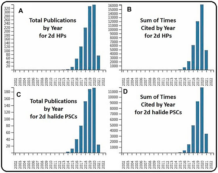
FIGURE 1. (A) Total publication by year for 2D halide perovskites. (B) Sum of time cited by year in the literature. (C) Total publication by year for 2D halide perovskite solar cells. (D) Sum of time cited by year in the literature.
Structural Aspects of 2D HPS: Engineered Energy Landscape
Microscopically layered HPs contain mono or a few thin atomic layers of HP (Gao et al., 2018). Atomically (morphologically) thin HPs or crystallographically layered HPs are considered as 2D/quasi-2D (q-2D) HPs. Dimensional confinement upon crystallization of HPs using the long-chain organic ligand-templated growth (Tyagi et al., 2015; Liu et al., 2017; Sheng et al., 2018) or self-templated growth (Ha et al., 2014; Liu et al., 2016; Niu et al., 2016), preserving the ABX3 formula, results in morphological 2D/q-2D HPs. Using bulky organic separators and by slicing 3D HPs along ⟨100⟩, ⟨110⟩, and ⟨111⟩ crystal planes, three different layered crystallographic 2D/q-2D HPs are obtained. As a consequence, the chemical formulae of 2D HPs are modified methodically according to the number of layers and crystal plane orientation. The chemical formula of A2′An−1BnX3n+1 specifically belongs to ⟨100⟩, A2′AmBmX3m+2 ⟨110⟩, and A2′Aq−1 BqX3q+3 ⟨111⟩ oriented HP family, respectively. The ⟨100⟩ oriented layered HP family, owing to its high acceptance to many distinct organic and inorganic components, is the most extensively investigated among them. The HP family oriented along the ⟨100⟩ direction is allocated further into two subcategories, the RP and Dion–Jacobson (DJ) (Ortiz-Cervantes et al., 2019) types. However, the DJ HPs are not often studied and applied in practical devices and are thus less popular in the device field (Mao et al., 2018). The name of RP HPs is derived from their resemblance in crystal with inorganic Sr3TiO7 RP perovskites (Ruddlesden and Popper, 1958). To put emphasis on the comparison in the crystal structure of HPs, we will focus our discussion on a schematic. Figure 2A describes the schematic of the 3D structure and the [001] projections of conventional inorganic CsPbBr3 cubic and orthorhombic perovskite phases and RP phases as labeled by Yu et al. (2017). Here, the material Csn+1PbnBr3n+1 or CsBr(CsPbBr3)n is found to be composed of “n” layers of CsPbBr3 unit cells separated by an extra CsBr layer. The RP phases are considered as a repeatedly integral extrinsic stacking error, designed by shifting two neighboring CsPbBr3 units by an in-plane lattice vector (1/2 1/2) compared to each other. Figure 2B shows a comparison between experimental and simulated scanning TEM (STEM) images of typical domains in 2D nanosheets of CsPbBr3. The three panels compare perovskite I: 6-layer perovskite phase (upper panel), 1-layer n = 2 RP phase (middle panel), and perovskite II: 6-layer perovskite phase with −PbBr3 termination (bottom layer). From the figure, it is clearly observed that RP domains and perovskite domains are well connected in 2D nanosheets owing to their crystal structure similarity, and all of these domain boundaries aligned in the ⟨100⟩ direction at the atomic scale. The details of the STEM mode of operation/characterization will be discussed in the next section.
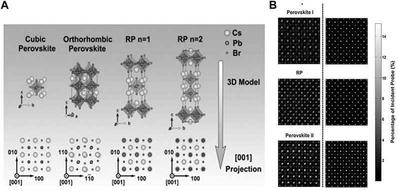
FIGURE 2. (A)Upper panel: conventional crystallographic structure of cubic and orthorhombic CsPbBr3 perosvskite phases along with RP phases (for different values of n = 1 and n = 2). Lower panel: unit cells and their projections along the [001] direction. (B) Atomic structures of the domains (plausible RP) and the domain boundaries (between the phases of conventional perovskites and RP) and the comparison between the experimental and simulated STEM images. Pure Cs and mixed Pb–Br cation columns are present along the [001] projected direction in conventional 3D structures of perovskite phases, as compared to the all-mixed Cs–Pb–Br cation column in RP phases along the same projected direction. The figure is reprinted with permission from Yu et al. (2017), copyright 2017, American Chemical Society.
For clarity, the general formula for 2D hybrid RP perovskites can be rewritten as (RNH3)2MX4 or (NH3RNH3)MX4, where M is the metal cation including Pb+2, Cu+2, and Sn+2 and R is the prototype organic molecule, for example, phenethylammonium (PEA) or butylammonium (BA) (Mitzi, 2001). In hybrid RP perovskites, an extraordinary ability to regulate the thickness of the inorganic layers is found, which is a highly needed characteristic for PV applications, specifically SCs. As a consequence, RP perovskites are found to be the most used and studied. For the construction of the few interconnected layers of corner-sharing M-X6 octahedra in q-2D HPs, the short-chain inorganic or organic cations are required. The value of “n” in the general formulae considered here is the number of layers in 2D and q-2D HPs. For n = 1, we get the 2D HPs. q-2D HPs are obtained for n ≥ 2. The intrinsically insulating large organic layers induce multiple QW structures (Chen C. et al., 2019) in between the assemblies of these organic layers with M-X6 octahedron layers. As a result, the 2D and q-2D RP HPs are found to exhibit electronic and quantum confinement even in thin films (Ding et al., 2018; Spanopoulos et al., 2019). A comparison between the 2D and 3D networks of perovskites and the modified band structure has been described by Straus and Kagan (2018). Figure 3A describes the projection of the 3D hybrid perovskite structure. It highlights an inorganic linkage of corner-sharing octahedral metal halide marked by red color, while the interstitial organic cations are marked with blue and black colors. The green color region emphasizes the limit on cation size. A projection down the c-axis of the 2D hybrid perovskite is schematically depicted in Figure 3B. It shows the successive arrangement of organic layers as shown in blue and black colors and the red inorganic layers that share the corners. The thickness of the inorganic and organic layers is marked as d and L, respectively, for n = 1. Here, the green region emphasizes the restriction on the area of cross section but not on the organic cation length. The energy band diagram of 2D structures, valence band (VB), conduction band (CB), electronic bandgap (Eg), and optical or excitonic bandgap Ex (blue color) are labeled in Figure 3C. The organic framework (with a lager HOMO–LUMO gap) has a dielectric constant ϵ2, while the inorganic slabs have a ϵ1 (ϵ1 > ϵ2). A dielectric confinement effect is originated by the alternation of a low dielectric constant of the organic moiety and a high dielectric constant of the Pb+2 halide layers (Ishihara et al., 1989; Koh et al., 2017). In 2D perovskites, due to a dielectric confinement effect in the layers, the electrons are strongly attracted to the holes. They attribute higher exciton binding energies for 2D perovskites than for their 3D counterpart.
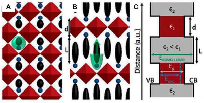
FIGURE 3. (A) Projection schematic of the 3D HP (color codes are as follows: red describes a corner-shared inorganic network of octahedral metal halide, blue and black describes the interstitial position of the organic cations, and green emphasizes the size restriction on cations). (B) Projection of the 2D HP along the c-axis (color codes are as follows: blue and black represents the organic alteration, red represents the corner-shared inorganic layers, and green represents the restriction on area cross section of organic cation and not on the length). d = inorganic layer thickness and L = organic layer thickness for n = 1. (C) Energy band diagram of 2D HP structures (Eg and Eexc denote the electronic and optical bandgap). Blue color represents the Eexc. The figure is reprinted with permission from Straus and Kagan et al. (2018), copyright 2017, American Chemical Society.
For SC application, the exciton binding energy should be as small as possible. The Pb HPs (that includes Lead as an element) with n ≥ 3, have bandgap, Eb comparable to 3D perovskites the dielectric constant increases largely with n, are able to perform decently as SC absorbers (Pazoki and Edvinsson, 2018). The bandgap is one of the most crucial parameters in SC applications. It determines the maximum theoretical efficiency for the corresponding single p–n junction device according to the Shockley–Queisser limit (Rühle, 2016). A bandgap of 1.34 eV results in a power conversion efficiency (PCE) of about 33.5% (Rühle, 2016; Slavney et al., 2017), while materials with bandgaps >1.9 eV are found to be the smart choice for tandem SCs. The bandgap for 2D HPs is typically determined by the composition and thickness of the inorganic layers. The bulkier halides lessen the bandgap. For n = 1, 2D perovskites with the formula (PEA)2PbX4 have bandgaps of about 3.8, 3.0, and 2.5 eV for Cl−, Br−, and I−, respectively (Kitazawa, 1997). The heavier, less electronegative halides have more delocalized electronic density, and it better overlaps with that of the metal atoms (Slavney et al., 2017). Therefore, halide substitutions can be a method for systematically engineering the bandgap of 2D hybrid HPs by adjusting the composition of their chemical constituents. The procedure allows broad absorption across the visible and near-infrared regions of wavelengths. The other method of bringing about the bandgap and photoluminescence (PL) wavelength modification is by changing the n value. With increase in n, the bandgap becomes smaller and tends toward the bandgap value of 3D perovskites as n approaches ∝, and the PL peak shifts asymptotically toward lower energies with increase in n (Stoumpos et al., 2017). Again, the coefficient of absorption (COA) is directly proportional to the strength of electronic dipole transitions. In 2D perovskites, light absorption is lesser due to a low density of metal/halogen atoms causing a lower absorption cross section. The COA increases rapidly as the n value increases. 2D perovskites with n ≥ 3 are comparable to 3D perovskites and have a high enough COA to harvest most of the incoming radiation. Following the trend, a general scaling law was proposed to determine the binding energy of Wannier–Mott excitons in perovskite QWs of arbitrary layer thickness (Blancon et al., 2018). In another approach (Mitzi et al., 1995), modified orientation of the conducting perovskite layers through choice of organic cation has been achieved. Interestingly, they found conducting layered organic–inorganic halide containing <110> oriented perovskite sheets. Here, it must be mentioned that surface modification also plays a critical role in device engineering. It was also observed that the layer edge electrons which are not related to the surface charging effect but associated with the local energy states correspond to the edge of the electronic structure (Wang et al., 2019). Therefore, in the next section, the focus of discussion is the characterization of the engineered 2D HP energy landscape and extrapolation of these specific features toward device application.
Microstructural Characterization of 2D HP: Optimization of Device Functionality
Crystallographic Characterization
Conductivities and carrier mobilities of layered 2D perovskites depend on the crystallographic direction. Generally, the conductivity and mobility are found to be significantly improved when measured along the planes of the inorganic layers. TEM and X-ray crystallographic techniques help to understand the device crystalline feature needed for improved device performance. Thus, a comparative structural study of 3D and 2D HPs has been given in this section.
The specific interactions between an electron beam with high energy and a thin electron-transparent sample are captured as the contrast of TEM images [already discussed in Figure 2 of earlier section]. High-resolution (resolution ∼ atomic scale) imaging can be achieved in the STEM mode, with few detectors to generate the images (e.g., BF: bright field, ADF: annular dark field, and HAADF: high-angle annular dark field). The crystallographic information is extracted from the electron diffraction patterns (EDPs) of the area of interest in the specimen understudy. Due to the modification of Bragg conditions in thin films, EDPs suffer from 2D imprecise crystallographic data. Energy-dispersive spectroscopy (EDS) and electron energy loss spectroscopy (EELS) yield the site-specific chemical composition information. EELS allows us to gather evidence about a range of sample-related aspects, such as thickness, chemical surrounding, bonding, and bandgap. (Virdi et al., 2016; Yu et al., 2017). On the other hand, novel EDS detectors allow efficient collection of specimen compositional data even at the atomistic scale. In a recent review, the beam sensitivity of HPs that guides the TEM characterization has been thoroughly discussed (Chen and Gao, 2020). For beam-sensitive HP materials, leading beam-damage mechanisms involve phonon-mediated heating, displacement of atoms and defect formation, that is, knock-on damage, and damage by inelastic scattering and rupture of chemical bonds, that is, radiolysis (Egerton et al., 2004). Several approaches such as optimizing the accelerating voltage and low-dose imaging with improved cameras can be employed to overcome degradation in beam-sensitive materials. The photon-induced dynamics and polarization of MA+ ions can affect the physical properties and device performance of MAPbI3 HPs. Thus, the photon-induced dynamics of MA+ is a major challenge for direct imaging of organic cations in TEM. Using an iterative cross-correlation–built algorithm on the filtered images, Zhang D. et al. (2018) successfully observed the ordered nanoscale domains with off-centered MA+ cations with differing orientations in MAPbBr3 crystals. The MA+ cations are found to exhibit configurations along the normal and parallel relative to the projection direction, forming in-plane and out-of-plane electric dipoles, respectively. Accordingly, the structural models and the corresponding simulated projected potential describe that the local deviations in the MA+ orientation are responsible for ferroelectricity and/or polarization in hybrid HPs. The crystal network of hybrid HPs is much ‘‘softer’’ than that of conventional oxide perovskites. As a result, there is a high probability of local vibrations in structures, modification in structures, and symmetry of the crystals. Thus, to visualize the pristine structure of a CsPbBr3 perovskite prepared via a catalyst-free solution-phase method (Yu et al., 2016), Yu et al. employed high-resolution TEM (HRTEM) in addition to small-dose in-line holography. The specimen under observation exhibited an atomically layered 2D nanosheet morphology. Employing focal series, they showed the existence of dual phases of CsPbBr3 cubic and orthorhombic HPs within the nanosheets. TEM can also identify the misalignment between the successive grains and even describe the boundary plane. Twin boundaries in MAPbI3 HP were identified by Rothmann et al. (2017) using TEM. These twin boundaries in specimens can originate during growth, phase transition, or even under mechanical stress. As HPs exhibit extreme chemical sensitivity, etching using a chemical solution is not a viable method for observing twin boundaries. Thus, electron back-scattered diffraction (EBSD) and TEM are essential tools for revealing twinning in HPs. Based on low-dose TEM imaging and selected area EDPs (SAEDPs), Rothmann et al. showed the presence of twinning in tetragonal MAPbI3, where these boundaries appeared in the form of parallel striped bands of few hundred nanometer width within MAPbI3 grains, although the device performance upon incorporation of the material was not clearly described by them. However, another recent study has pointed out that twin boundaries can be very effective in restricting photocarriers (Li M. et al., 2018; Li W. et al., 2018). The other report (Bertolotti et al., 2017) prompted flexibility of HP nanocrystals (NCs) upon halide changes and temperature variation, which has been investigated following high-resolution synchrotron X-ray total scattering data. Variations in the local structure of these NCs were found to exhibit orthorhombic tilting of PbX6 octahedra within locally ordered subdomains. These subdomains are linked by a 2D/3D network of twin boundaries through which the coherent arrangement of the Pb+ over the whole NC is preserved. Thus, we believe that controlling the properties of twinning (size, orientations, etc.) could be a viable approach for achieving and modifying the characteristics of newly designed HPs.
The grain-boundary chemistry in PSCs intensely influences carrier recombination and potential transport of ionic and molecular species, thus affecting the optoelectronic properties and chemical stability of HPs. The grain-boundary chemistry of HPs depends on the HP bulk elemental composition, growth conditions, the structure and the kinetics of the boundary, and careful chemical modifications. In a contemporary study (Zong et al., 2018), triblock copolymer (Pluronic 123P) functionalized MAPbI3 HPs were found to result in water-resistant HPs. The copolymer establishes the interaction with HP grains via its hydrophilic tails, while its hydrophobic core is placed toward the center of the copolymer wetting film. As a consequence, a water-resistant HP with higher stability was obtained.
Morphological and Conductive Characterization: Scanning Probe Microscopy
Scanning probe microscopy, including AFM, Kelvin probe force microscopy (KPFM), and conductive AFM (C-AFM), has been broadly applied to explore the local physical, electromagnetic, or molecular topographies at a microscopic scale. AFM and KPFM are two different modes of microscopic technique that operate under constant or variable bias conditions. Specifically, KPFM captures the contact potential difference (CPD) between the conductive tip and the sample (Chen Z. et al., 2019). Under an alternative voltage, the CPD is measured by using a vibrating capacitor with the Kelvin method (Benstetter et al., 2017). Instead of the current, the sensitivity of KPFM is improved by recording the electrostatic force interaction between the tip and the sample. By accurate adjustment of the tip work function on the reference sample, the other materials’ surface work function can be determined (Shao et al., 2016). In high-resolution C-AFM (Yang et al., 2009; Shin et al., 2013), the current–voltage characteristics of the sample surface could be easily captured by the mapping of the topography. A large current flow points toward high conductivity of the sample and a strategic character of the charge transport (Bristowe et al., 2015; Wang et al., 2016; Si et al., 2017; Lee et al., 2018; Xu et al., 2018; Eichhorn et al., 2018). Thus, by C-AFM, the conductivity difference among dissimilar perovskite films can be captured and their transport characteristics (at grain boundaries and in grain interiors) can be distinguished with the nanoscale resolution. Even for phase-pure perovskites where compositional engineering is used to overcome difficulties in obtaining high-quality samples, ambient instability degrades the device performance. Lee et al., reported the fabrication of phase-pure formamidinium-lead tri-iodide (FAPbI3) perovskite films with excellent optoelectronic quality and stability. They showed that incorporation of 1.67 mol% of 2D PEA lead iodide into the precursor solution allows the formation of phase-pure FA perovskites with an enhanced PL lifetime (Lee et al., 2018). Figure 4 describes the band alignment and local conductivity with 2D perovskites, as described by Lee et al.(2018). Figure 4A describes the device schematic comprising the polycrystalline film of a 3D perovskite with grain boundaries containing 2D perovskites, while Figure 4B describes the layer by layer Tauc plots and UV photoelectron spectroscopic analysis of the device band structure. The bare C-AFM images of FAPbI3 and with films of 2D perovskite on ITO glass coated with SnO2 are shown in Figure 4 (C, E) and (D, F), respectively. A 100- mV bias voltage was applied to get the images under the room light condition for image (C, D) and low light intensity condition for image (E, F), as provided by the setup. The topology of each film is depicted in the inset of the corresponding images. For (C, D) and (E, F), the corresponding scale bars are shown at the left and right sides, respectively. It describes that under ambient light conditions, the flow of current in the perovskite film with 2D perovskite was higher at/near the grain boundaries while a fairly uniform flow of current was noted in the bare FAPbI3 film. With light illumination, the flow of current was further enhanced at/near the grain boundaries with the 2D perovskite, whereas the current flow the in bare FAPbI3 film was uniformly increased, which indicates that separation of charge and collection of photo-generated electrons are more favorable at the grain boundaries with the 2D perovskite. On the other hand, the 2D (PEA)2PbI4 perovskite with aromatic rings and longer alkyl chains is projected to be more resilient to moisture. It guards the defective grain boundaries of the 3D perovskite, resulting in the significantly improved moisture stability of the film. Regardless of the improved stability, degraded electronic properties of the film are expected due to the poor charge carrier mobility of the 2D perovskite. Interestingly, a report by Wang et al. highlighted a prominent conducting feature, observed at the layer edges between the insulating bulk regions of the (BA)2PbI4 2D perovskite single crystal. In the bulk region, the electron–hole pairs are tightly bonded. At the layer edges, additional edge state (ES) electrons are located, which control the current detected by the C-AFM measurement (Wang et al., 2019). These observations of the metal-like conducting feature at the layer edge of the 2D perovskite offer a different dimension for improving the performance of the next-generation optoelectronics and innovative nanoelectronics. Piezo-response force microscopy (PFM) is an AFM-based method depending on the inverse piezoelectric effect, analyzing the local electromechanical properties of piezoelectric samples. Remarkably, PFM has been widely employed to study the possible ferroelectricity in the MAPbI3 perovskite (Fan et al., 2015). The theoretical calculations suggested the presence of a ferroelectric domain in the perovskite samples that would result in the separation of photoexcited electron–hole pairs making an internal junction. It allows the reduction of recombination through the segregation of charge carriers. PFM also ascertains the ferroelectric features in other 2D layered perovskite materials (Sha et al., 2019; Chen and Gao, 2020) which are useful as sensors in flexible devices, soft robotics, and biomedical devices, a great influence toward next-generation devices. However, the ferroelectricity of MAPbI3 is still under debate (Wang et al., 2017).
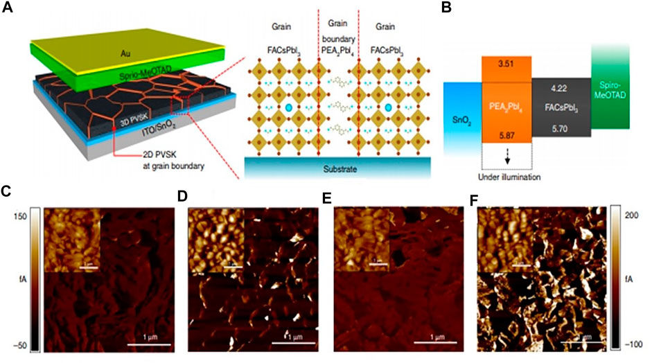
FIGURE 4. Local conductivity and band alignment in the 2D perovskite. (A) The device schematic comprising polycrystalline film of the 3D perovskite with grain boundaries containing the 2D perovskite. (B) The layer-by-layer Tauc plots and UV photoelectron spectroscopic analysis of the device band structure. The bare C-AFM images of FAPbI3(C, E) and with films of 2D perovskite (D, F) on ITO glass coated with SnO2. 100 mV bias voltage was applied to get the images under the room light condition for (C, D) and low light intensity condition for (E, F), as provided by the setup. Topology of each film is depicted in the inset of the corresponding images. For (C, D) and (E, F), the scale bars are shown at the left and right sides, respectively. The figure is reprinted with permission from Lee et al. (2018), copyright 2018, Nature Publishing Group.
Here, we would like to mention that other than conventional microscopic techniques, microwave photoconductivity imaging (MIM) on MAPbI3 has been proven to be an efficient technique for quantitative estimation of photoconductivity. A recent report highlighted the nanoscale photoconductivity imaging of two MAPbI3 thin films with different efficiencies by light-stimulated microwave impedance microscopy (Chu et al., 2017). Here, unlike the C-AFM technique, direct contact between the MIM tip and the perovskite thin films is not required. The effective capacitive coupling between the MIM tip and the perovskite thin films at GHz frequencies overcomes the difficulties of nanoscale electrical properties on samples with a capping layer which is insulating in nature.
Distinctive Spectroscopic Characteristics: A Route to Device Functionality
The two most general schemes practiced to enhance the PCE of 2D and q-2D HP-based SCs are (i) optimizing the layer numbers (n) to get adequate absorption of light and charge generation and (ii) refining the crystallographic alignment for better charge transport to the electrode. Although the layer number can be easily modified by tuning the composition of 2D and q-2D HPs in precursors, the controlled orientational growth remains a big challenge. Noninvasive spectroscopic approaches are the easiest for probing these distinctive characteristics of the 2D perovskite specimens compared to conventional microscopic techniques, as here we do not need any sample preparation. Here, we will discuss a general scaling law that was proposed by Blancon et al. (2018) to determine the binding energy of Wannier–Mott excitons in perovskite QWs of arbitrary layer thickness. Figure 5 describes the absorption and PL, that is, the optical spectroscopic feature of the 2D and q-2D HP crystals, having n = one to five for inorganic RP perovskite QWs following the reference (Blancon et al., 2018). It specifically highlights (A) scaling of experimentally obtained optical bandgap and (B) PL spectra for the material. This understanding provides direct insight about the photophysics of RP perovskite materials utilized in practical devices.
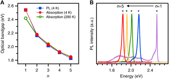
FIGURE 5. Optical spectroscopy, PL (at 4 K blue square symbol and line), and absorption spectra (at 4 K red and 290 K green closed and opened circle) of the RP perovskite crystals with n = 1–5. (A) Scaling of experimentally obtained optical bandgap. (B) Photoluminescence spectra. The figure is reprinted with permission from Blancon et al. (2018), copyright 2018, Nature Publishing Group.
Generally, in 3D HPs, excited charges diffuse quicker than the radiative recombination rate. Thus, most of them are confined at the grain-boundary defects. However, in 2D HPs, free charges and excitons coexist in a small regime, enhancing the radiative combination relative to the bulk specimen. Due to the surface and interface defects present in the sample, the nonradiative recombination still controls the energy transfer phenomena and the PL in 2D HPs remains comparatively low. It is evident from these results that layered HPs might not be a good choice for LEDs when one considers high brightness and effective quantum efficiency (EQE). However, owing to their excellent stability and processing ability, they are considered to be the finest candidates for practical LEDs (Chiba et al., 2018; Yang et al., 2018; Xu et al., 2019).
Metal HPs also show the necessary optical–electrical characteristics for PV devices, such as long carrier diffusion lengths, high carrier mobility, and strong and broad optical absorption, all of which support the notable PCE of the device. In general, 2D flakes of MAPbI3 are a widely accepted active material for photodetectors for its large COA, high mobility of the carrier, and smaller exciton binding energy (<26 meV, room temperature). 2D RP perovskites are also known to exhibit excellent photodetection performance. In a recent report, Zhou et al. (2016) explained that the RP perovskite film displayed the layer number–dependent response spectrum, which is compatible with their absorption spectrum. As the perovskite films are configured into photodetectors, a better photodetection property was detected in the film with the higher n value. Here, the polycrystalline nature of 2D RP perovskites might be the cause behind the observed lower photoresponse. In recent times, the photodetection ability of 2D RP perovskites was observed to be considerably upgraded by the replacement of the long direct chain n-BA+ with branched i-BA+ using a method of hot-casting processing (Dong et al., 2019).
The functionality of the devices is mostly dependent on the grain structure of polycrystalline 2D perovskites, but in situ, chemically specific characterization of 2D perovskite grains is currently limited. Here, the polarized ultralow-frequency Raman microspectroscopy is found to be a simplistic yet influential tool for identifying relative grain orientations in 2D perovskite thin films (Toda et al., 2020). Even from temperature-dependent PL spectra of 2D perovskites and following the generalized Elliot formula, the evidence of phonon-assisted sidebands is explained by Feldstein et al. (2020). They determined the spectral linewidth of the energetically lowest excitonic transitions in view of the scattering channels, focusing on the emission and absorption of phonons (low-energy acoustic and higher energy optical) (Feldstein et al., 2020). The low-energy, heat-carrying acoustic phonons play the central role in the management of heat in 2D RP–supported devices, which remained unexplored for a long time. A recent study by Guo et al. (2018) discusses the generation and transmission of coherent longitudinal acoustic phonons along the 2D RP cross-plane direction, resulting in distinct characterizations of lower bandgap refractive indices. They have demonstrated a significant drop in group velocity and propagation length of acoustic phonons in 2D RPs compared to the 3D MAPbI3 counterpart (Guo et al., 2018). The observed vibrational feature is a consequence of the large acoustic impedance disparity between the successive layers of perovskite and large organic cations.
Pump-probe spectroscopy offers a feasible way to identify the carrier dynamics in the 2D perovskite materials (Giovanni et al., 2018). Transient absorption microscopy (TAM) (Williams et al., 2019) is one of the techniques employed to probe the diffusion of the carrier and two-body recombination processes. Figure 6, as reproduced following Williams et al. (2019), describes the schematic of the concentration distribution of QWs that yields a gradient in excitation frequencies and enables a unidirectional flow of energy as a cascade, obtained by TAM. Figure 6A describes the concentration gradient of QWs throughout a film of layered perovskite. According to the idea, the glass edge of the perovskite film is highly populated with the smallest QWs and the air edge is mostly dense with the thickest QWs. Figure 6B schematically highlights the diagram describing the down-hill energy transfer cascade. It is observed that the excitonic resonances of the QWs decrease with an increase in thickness and the direction of electron transfer is the same as that of energy transfer as compared to the holes which are moving toward the states of higher energy. For applications such as microcavity lasers, boosting of the two-body recombination processes is desirable. Here, a methodical comparison of the layered films of (PEA)2 (MA)n−1 [PbnI3n+1] with phase-pure single crystals discloses that diffusion is blocked by grain boundaries in the films, stimulating two-body recombination. The energy transfer rules the sub-200 ps timescale, and the energy levels of the quantum wells are organized such that hole transfer may take place from the air to glass sides of the film at future times. The high-performance nanolasers made up of perovskites have attained low threshold, high-quality factor, and tunable wavelengths under optical excitation (Guo et al., 2018; Zhang H. et al., 2018; Liu et al., 2020). Their compact volume could entrap the light field in a tiny region and improve the light–matter interactions. Another interesting report established that QWs of colloidal lead halide perovskites can produce fully decoupled multi-QW (MQW) superlattices (having intralayer local exciton) with ultrathin organic quantum barriers (Jagielski et al., 2020), same as the addition of monolayer hybrid BN (h-BN). The obtained result demonstrates that photonic sources have emission of narrowband, high quantum yield, improved light outcoupling, and wavelength tenability useful for nano-antennas (near field) and LEDs (far field). Even theoretically, it was proposed (Li et al., 2020) that the use of superlattice structures is a smart approach (such as mixing of cations and partial substitution of halogens by superhalogens) for expanding the family of perovskites and obtaining excellent optoelectronic materials with improved stability.
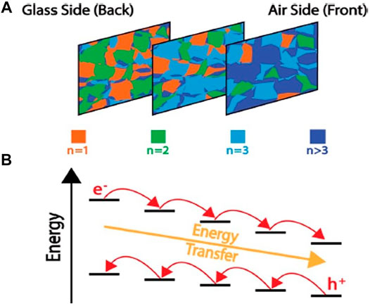
FIGURE 6. (A) Concentration gradient of quantum wells (QWs) throughout a film of layered perovskite is depicted here. The glass edge of the perovskite film is highly populated with the smallest QWs and the air edge is mostly dense with the thickest QWs. (B) Schematic diagram describing the down-hill energy transfer cascade. Excitonic resonances of the quantum wells decrease with the increase in thickness. The direction of electron transfer is the same as that of energy transfer, as compared to the holes which are moving toward the states of higher energy. The figure is reprinted with permission from Williams et al. (2019), copyright 2019, American Chemical Society.
The VB of 2D perovskites predominantly consists of halide p-orbitals hybridized with metal s-orbitals, and a CB is dominated by metal p-orbitals. In Pb HPs, the corresponding orbitals are 5p of I and 6s and 6p of Pb (Even et al., 2012; Even et al., 2013; Gebhardt et al., 2017). In 2D HPs, the existence of Pb and I prompts a large spin-orbit coupling (SOC) which in the presence of structural inversion asymmetry boosts the spin-degeneracy of the CB and VB (Kepenekian et al., 2015; Kepenekian and Even, 2017). It seems that 2D perovskites self-assemble into regular QW structures that break the symmetry of the 3D system. It amplifies the Rashba effect and escalates their potential for opto-spintronic applications, as observed by transient spectroscopic measurements (Zhai et al., 2017). The rate of charge carrier recombination and spin-coherence lifetimes of 2D RP perovskite single crystals PEA2PbI4/(MAPbI3)n−1 (with n = 1, 2, 3, 4) have been reported by Chen et al. (2018). Charge carrier recombination rates are observed to be fastest for n = 1 due to the large exciton binding energy and the slowest for n = 2. Spin-coherence times at ambient temperature also demonstrate a non-monotonic layer thickness dependency with a growing spin-coherence lifetime, which increases for n = 1 to n = 4, followed by a reduction in lifetime for n = 4 to ∞. For n = 4, the longest coherence lifetime of ∼7 ps was detected. Their observations are dependent on two contributions: (a) Rashba-splitting increasing the spin-coherence lifetime for the n = ∞ to the smaller layered systems and (b) phonon-scattering increases for smaller layers, reducing the spin-coherence lifetime. The interplay between these two contributions modifies the layer thickness dependency. Here, they also measured the carrier dynamics by the exciton bleach kinetics and the spin-coherence dynamics by employing circularly polarized pump and probe pulses.
From the above discussion, we can extract that for device application, a stable structure is the most feasible. Figure 7 describes that the dimensional reduction and modified/engineered surface needed for stable 2D HP device functionality. Remarkably, a report by Grancini et al. (2017) introduced a stable perovskite device by engineering a (HOOC(CH2)4NH3)2PbI4/CH3NH3PbI3 2D/3D perovskite junction. The unique gradually organized 2D/3D multidimensional interface produces up to 12.9% efficiency in carbon-based architecture and ∼14.6% in standard mesoporous SCs for 1 year. Their innovative, low-cost, and stable architecture has supported the timely commercialization of PSCs. Thus, we propose that a detailed microstructural analysis of 2D HPs is the much-needed approach to engineer new materials for energy research application, especially SCs. In this review, we have tried to sum up the characteristics of 2D HPs reported/proposed to have stable architecture feasible for energy research application.
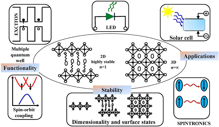
FIGURE 7. Schematic representation of stability and functionality of 2D HPs.
Conclusion
This review shows that for commercialization of HP optoelectronic devices, a thorough in-depth characterization of 2D HP materials is essential. The most unique features for the light-absorbing layers of SCs related to this type of material are their optimized dielectric constants and exciton binding energy compared to conventional semiconductors, and it also include a rotational component connected with the relaxation of the molecular dipole. Although great efforts have been made to study various 2D HP materials, many challenges are still there where utilizing these materials in actual practical purposes is concerned. But, the fabricated devices using 2D HPs are still facing a degradation problem. More experimental and theoretical studies are needed in this regard to understand the degradation and improve the stability. On the other hand, there is a critical need for an improved procedure of synthesis of single crystals of 2D HP with controlled thickness and large dimension. The above discussion highlights the correlation between the microscopic, crystallographic, and molecular structures of 2D layered HP, and it is expected that these photoresponse properties of the material will be further corroborated toward developing flexible, functional, and tunable optoelectronics devices in the future.
Author Contributions
SB and GC designed and wrote the manuscript. PP supervised this work and revised the manuscript. All authors contributed to the article and agreed on the submitted version.
Funding
This work was supported by the Faculty Research Grant (NITC/DEAN(R&C)/FRG/2018–19/3), NIT Calicut and ANERT (ANERT-TECH/11/2019S(NEP)), Govt. of Kerala, Kerala.
Conflict of Interest
The authors declare that the research was conducted in the absence of any commercial or financial relationships that could be construed as a potential conflict of interest.
References
Anasori, B., Xie, Y., Beidaghi, M., Lu, J., Hosler, B. C., Hultman, L., et al. (2015). Two-Dimensional, Ordered, Double Transition Metals Carbides (MXenes). ACS Nano. 9 (10), 9507–9516. doi:10.1021/acsnano.5b03591
Benstetter, A. H. G., Liu, D., Frammelsberger, W., and Lanza, M. (2017). Conductive Atomic Force Microscopy: Applications in Nanomaterials. Hoboken: Wiley-VCH Verlag GmbH & Co. KGaA.
Bertolotti, F., Protesescu, L., Kovalenko, M. V., Yakunin, S., Cervellino, A., Billinge, S. J. L., et al. (2017). Coherent Nanotwins and Dynamic Disorder in Cesium lead Halide Perovskite Nanocrystals, ACS Nano. 11, 3819–3831. doi:10.1021/acsnano.7b00017
Blancon, J.-C., Tsai, H., Nie, W., Stoumpos, C. C., Pedesseau, L., Katan, C., et al. (2017). Extremely Efficient Internal Exciton Dissociation through Edge States in Layered 2D Perovskites, Science 355, 1288–1292. doi:10.1126/science.aal4211
Blancon, J. C., Stier, A. V., Tsai, H., Nie, W., Stoumpos, C. C., Traoré, B., et al. (2018). Scaling Law for Excitons in 2D Perovskite Quantum wells. Nat. Commun. 9, 2254. doi:10.1038/s41467-018-04659-x
Bristowe, N. C., Varignon, J., Fontaine, D., Bousquet, E., and Ghosez, P. (2015). Ferromagnetism Induced by Entangled Charge and Orbital Orderings in Ferroelectric Titanate Perovskites. Nat. Commun. 6, 6677. doi:10.1038/ncomms7677
Chen, S., and Gao, P. (2020). Challenges, Myths, and Opportunities of Electron Microscopy on Halide Perovskites. J. Appl. Phys. 128, 010901. 10.1063/5.0012310
Chen, C., Song, Z., Xiao, C., Zhao, D., Shrestha, N., Li, C., et al. (2019). Achieving a High Open-Circuit Voltage in Inverted Wide-Bandgap Perovskite Solar Cells with a Graded Perovskite Homojunction. Nano Energy. 61, 141–147. doi:10.1016/j.nanoen.2019.04.069
Chen, T., Foley, B. J., Ipek, B., Tyagi, M., Copley, J. R. D., Brown, C. M., et al. (2015). Rotational Dynamics of Organic Cations in the CH3NH3PbI3perovskite. Phys. Chem. Chem. Phys. 17, 31278–31286. doi:10.1039/C5CP05348J
Chen, X., Lu, H., Li, Z., Zhai, Y., Ndione, P. F., Berry, J. J., et al. (2018). Impact of Layer Thickness on the Charge Carrier and Spin Coherence Lifetime in Two-Dimensional Layered Perovskite Single Crystals. ACS Energ. Lett. 3, 2273–2279. doi:10.1021/acsenergylett.8b01315
Chen, X.-G., Song, X.-J., Zhang, Z.-X., Li, P.-F., Ge, J.-Z., Tang, Y.-Y., et al. (2020). Two-dimensional Layered Perovskite Ferroelectric with Giant Piezoelectric Voltage Coefficient. J. Am. Chem. Soc. 142 (2), 1077–1082. doi:10.1021/jacs.9b12368
Chen, Z., Guo, Y., Wertz, E., and Shi, J. (2019). Merits and Challenges of Ruddlesden–Popper Soft Halide Perovskites in Electro-Optics and Optoelectronics. Adv. Mater. 31, 1803514. doi:10.1002/adma.201803514
Chiba, T., Hayashi, Y., Ebe, H., Hoshi, K., Sato, J., Sato, S., et al. (2018). Anion-exchange Red Perovskite Quantum Dots with Ammonium Iodine Salts for Highly Efficient Light-Emitting Devices. Nat. Photon. 12, 681–687. doi:10.1038/s41566-018-0260-y
Chu, Z., Yang, M., Schulz, P., Wu, D., Ma, X., Seifert, E., et al. (2017). Impact of Grain Boundaries on Efficiency and Stability of Organic–Inorganic Trihalide Perovskites. Nat. Commun. 8, 2230. doi:10.1038/s41467-017-02331-4
Correa-Baena, J.-P., Saliba, M., Buonassisi, T., Grätzel, M., Abate, A., Tress, W., et al. (2017). Promises and Challenges of Perovskite Solar Cells. Science 358, 739–744. doi:10.1126/science.aam6323
Ding, Y.-F., Zhao, Q.-Q., Yu, Z.-L., Zhao, Y.-Q., Liu, B., He, P.-B., et al. (2019). Strong Thickness-dependent Quantum Confinement in All-Inorganic Perovskite Cs2PbI4 with a Ruddlesden–Popper Structure. J. Mater. Chem. C 7, 7433–7441. doi:10.1039/C9TC02267H
Dong, R., Lan, C., Xu, X., Liang, X., Hu, X., Li, D., et al. (2019). Novel Series of Quasi-2D Ruddlesden-Popper Perovskites Based on Short-Chained Spacer Cation for Enhanced Photodetection. ACS Appl. Mater. Int. 10 (22), 19019–19026. doi:10.1021/10.1021/acsami.8b03517
Egerton, R. F., Li, P., and Malac, M. (2004). Radiation Damage in the TEM and SEM. Micron 35, 399–409. doi:10.1016/j.micron.2004.02.003
Eichhorn, J., Kastl, C., Cooper, J. K., Ziegler, D., Schwartzberg, A. M., Sharp, I. D., et al. (2018). Nanoscale Imaging of Charge Carrier Transport in Water Splitting Photoanodes. Nat. Commun. 9, 2597. doi:10.1038/s41467-018-04856-8
Even, J., Pedesseau, L., Dupertuis, M.-A.-A., Jancu, J.-M.-M., and Katan, C. (2012). Electronic Model for Self-Assembled Hybrid Organic/perovskite Semiconductors: Reverse Band Edge Electronic States Ordering and Spin-Orbit Coupling. Phys. Rev. B 86, 205301. doi:10.1103/PhysRevB.86.205301
Even, J., Pedesseau, L., Jancu, J.-M.-M., and Katan, C. (2013). Importance of Spin-Orbit Coupling in Hybrid Organic/inorganic Perovskites for Photovoltaic Applications. J. Phys. Chem. Lett. 4 (17), 2999–3005. doi:10.1021/jz401532q
Fan, Z., Xiao, J., Sun, K., Chen, L., Hu, Y., Ouyang, J., et al. (2015). Ferroelectricity of CH3NH3PbI3 Perovskite. J. Phys. Chem. Lett. 6 (7), 1155–1161. doi:10.1021/acs.jpclett.5b00389
Feldstein, D., Perea-Causín, R., Wang, S., Dyksik, M., Watanabe, K., Taniguchi, T., et al. (2020). Microscopic Picture of Electron-Phonon Interaction in Two-Dimensional Halide Perovskites. J. Phys. Chem. Lett. 11 (23), 9975–9982. doi:10.1021/acs.jpclett.0c02661
Ferrari, A. C., Bonaccorso, F., Fal'ko, V., Novoselov, K. S., Roche, S., Bøggild, P., et al. (2015). Science and Technology Roadmap for Graphene, Related Two-Dimensional Crystals, and Hybrid Systems. Nanoscale 7, 4598–4810. doi:10.1039/C4NR01600A
Gao, P., Yusoff, A. R., and Nazeeruddin, M. K. (2018). Dimensionality Engineering of Hybrid Halide Perovskite Light Absorbers. Nat. Commun. 9, 5028. doi:10.1038/s41467-018-07382-9
Gao, H., Wei, W., Li, L., Tan, Y., and Tang, Y.. (2020). Mechanical Properties of a 2D Lead-Halide Perovskite, (C6H5CH2NH3)2PbCl4, by Nanoindentation and First-Principles Calculations, J. Phys. Chem. C, 124, 19204–19211. doi:10.1021/acs.jpcc.0c04283
Gebhardt, J., Kim, Y., and Rappe, A. M. (2017). Influence of the Dimensionality and Organic Cation on crystal and Electronic Structure of Organometallic Halide Perovskites. J. Phys. Chem. C 121 (12), 6569–6574. doi:10.1021/acs.jpcc.7b00890
Giovanni, D., Chong, W. K., Liu, Y. Y. F., Dewi, H. A., Yin, T., Lekina, Y., et al. (2018). Coherent Spin and Quasiparticle Dynamics in Solution-Processed Layered 2D Lead Halide Perovskites. Adv. Sci. 5 (10), 1800664. doi:10.1002/advs.201800664
Grancini, G., Roldán-Carmona, C., Zimmermann, I., Mosconi, E., Lee, X., Martineau, D., et al. (2017). One-Year Stable Perovskite Solar Cells by 2D/3D Interface Engineering. Nat. Commun. 8, 15684. doi:10.1038/ncomms15684
Guo, P., Stoumpos, C. C., Mao, L., Sadasivam, S., Ketterson, J. B., Darancet, P., et al. (2018). Cross-plane Coherent Acoustic Phonons in Two-Dimensional Organic–Inorganic Hybrid Perovskites. Nat. Commun. 9 (1), 2019. doi:10.1038/s41467-018-04429-9
Ha, S. T., Liu, X., Zhang, Q., Giovanni, D., Sum, T. C., and Xiong, Q. (2014). Synthesis of Organic–Inorganic Lead Halide Perovskite Nanoplatelets: Towards High-Performance Perovskite Solar Cells and Optoelectronic Devices. Adv. Opt. Mater. 2, 838–844. doi:10.1002/adom.201400106
Ishihara, T., Takahashi, J., and Goto, T. (1989). Exciton State in Two-Dimensional Perovskite Semiconductor (C10H21NH3)2PbI4. Solid State. Commun. 69, 933–936. doi:10.1016/0038-1098(89)90935-6
Jagielski, J., Solari, S. F., Jordan, L., Scullion, D., Blülle, B., Li, Y.-T., et al. (2020). Scalable Photonic Sources Using Two-Dimensional lead Halide Perovskite Superlattices. Nat. Commun. 11, 387. doi:10.1038/s41467-019-14084-3
Jiang, X., Kuklin, A. V., Baev, A., Ge, Y., Ågren, H., Zhang, H., et al. (2020). Two-dimensional MXenes: From Morphological to Optical, Electric, and Magnetic Properties and Applications. Phys. Rep., 848, 1–58. doi:10.1016/j.physrep.2019.12.006
Kamminga, M. E., Fang, H.-H., Filip, M. R., Giustino, F., Baas, J., Blake, G. R., et al. (2016). Confinement Effects in Low-Dimensional Lead Iodide Perovskite Hybrids. Chem. Mater., 28, 4554–4562. doi:10.1021/acs.chemmater.6b00809
Kepenekian, M., and Even, J. (2017). Rashba and Dresselhaus Couplings in Halide Perovskites: Accomplishments and Opportunities for Spintronics and Spin–Orbitronics. J. Phys. Chem. Lett. 8, 3362–3370. doi:10.1021/acs.jpclett.7b01015
Kepenekian, M., Robles, R., Katan, C., Sapori, D., Pedesseau, L., and Even, J. (2015). Rashba and Dresselhaus Effects in Hybrid Organic–Inorganic Perovskites: From Basics to Devices. ACS Nano. 9 (12), 11557–11567. doi:10.1021/acsnano.5b04409
Kitazawa, N. (1997). Excitons in Two-Dimensional Layered Perovskite Compounds: C6h5c2h4nh3)2pb(br,i)4 (C6h5c2h4nh3)2pb(cl,br)4. Mater. Sci. Eng. B 49, 233‒238. doi:10.1016/S0921-5107(97)00132-3
Koh, T. M., Febriansyah, B., and Mathews, N. (2017). Ruddlesden–Popper Perovskite Solar Cells. Chem 2, 326. doi:10.1016/j.chempr.2017.02.015
Lee, M. M., Teuscher, J., Miyasaka, T., Murakami, T. N., and Snaith, H. J. (2012). Efficient Hybrid Solar Cells Based on Meso-Superstructured Organometal Halide Perovskites. Science 338 (6107), 643–647. doi:10.1126/science.1228604
Lee, J.-W., Dai, Z., Han, T. H., Choi, C., Chang, S. Y., Lee, S. J., et al. (2018). 2D Perovskite Stabilized Phase-Pure Formamidinium Perovskite Solar Cells. Nat. Commun. 9, 3021. doi:10.1038/s41467-018-05454-4
Leguy, A. M. A., Frost, J. M., McMahon, A. P., Sakai, V. G., Kockelmann, W., Law, C., et al. (2015). The Dynamics of Methylammonium Ions in Hybrid Organic–Inorganic Perovskite Solar Cells. Nat. Commun. 6, 7124. doi:10.1038/ncomms8124
Li, D., Li, D., Zhang, H., Yang, A., and Chunjun Liang, C. (2020). High-Performance Photovoltaic Materials Based on the Superlattice Structures of Organic–Inorganic Halide Perovskite and Superhalogen Hybrid Perovskite. J. Phys. Chem. Lett. 11 (13), 5282–5294. doi:10.1021/acs.jpclett.0c01161
Li, M., Gao, Q., Liu, P., Liao, Q., Zhang, H., Yao, J., et al. (2018). Amplified Spontaneous Emission Based on 2D Ruddlesden–Popper Perovskites. Adv. Funct. Mater. 28 (17), 1707006. doi:10.1002/adfm.201707006
Li, W., Yadavalli, S. K., Lizarazo-Ferro, D., Chen, M., Zhou, Y., Padture, N. P., et al. (2018). Subgrain Special Boundaries in Halide Perovskite Thin Films Restrict Carrier Diffusion. ACS Energ. Lett. 3 (11), 2669–2670. doi:10.1021/acsenergylett.8b01704
Liu, J., Xue, Y., Wang, Z., Xu, Z.-Q., Zheng, C., Weber, B., et al. (2016). Two-dimensional CH3NH3PbI3 Perovskite: Synthesis and Optoelectronic Application. ACS Nano 10, 3536–3542. doi:10.1021/acsnano.5b07791
Liu, X.-D., Wang, Q., Cheng, Z.-Q., Qiu, Y.-H., Zhou, L., and Wang, Q.-Q. (2017). Solution-phase Growth of Organolead Halide Perovskite Nanowires and Nanoplates Assisted by Long-Chain Alkylammonium and Solvent Polarity. Mater. Lett. 206, 75–79. doi:10.1016/j.matlet.2017.06.113
Liu, Z., Huang, S., Du, J., Wang, C., and Leng, Y. (2020). Advances in Inorganic and Hybrid Perovskites for Miniaturized Lasers. Nanophotonics. 9 (8), 2251–2272. doi:10.1515/nanoph-2019-0572
Mao, L., Ke, W., Pedesseau, L., Wu, Y., Katan, C., Even, J., et al. (2018). Hybrid Dion-Jacobson 2D Lead Iodide Perovskites. J. Am. Chem. Soc. 140 (10), 3775–3783. doi:10.1021/jacs.8b00542
Mao, L., Stoumpos, C. C., and Kanatzidis, M. G.. (2019). .Two-Dimensional Hybrid Halide Perovskites: Principles and Promises. J. Am. Chem. Soc. 141, 1171–1190. doi:10.1021/jacs.8b10851
Mas-Ballesté, R., Gómez-NavarroGómez-Herrero, C., and Zamora, F. (2011). 2D Materials: to Graphene and beyond. Nanoscale 3, 20–30. doi:10.1039/C0NR00323A
Mitzi, D. B., Wang, S., Feild, C. A., Chess, C. A., and Guloy, A. M. (1995). Conducting Layered Organic–Inorganic Halides Containing <110>-Oriented Perovskite Sheets. Science 267 (5203), 1473–1476. doi:10.1126/science.267.5203.1473
Mitzi, D. B. (2001). Templating and Structural Engineering in Organic–Inorganic Perovskites. J. Chem. Soc. Dalton Trans. 1, 1–12. doi:10.1039/B007070J
Naguib, M., Kurtoglu, M., Presser, V., Lu, J., Niu, J., Heon, M., et al. (2011). Two Dimensional Nanocrystals Produced by Exfoliation of Ti3AlC2. Adv. Mater. 23 (37), 4248–4253. doi:10.1002/adma.201102306
Naguib, M., Mashtalir, O., Carle, J., Presser, V., Lu, J., Hultman, L., et al. (2012). Two-Dimensional Transition Metal Carbides. ACS Nano. 6 (2), 1322–1331. doi:10.1021/nn204153h
Niu, L., Zeng, Q., Shi, J., Cong, C., Wu, C., Liu, F., et al. (2016). Controlled Growth and Reliable Thickness-dependent Properties of Organic–Inorganic Perovskite Platelet Crystal. Adv. Funct. Mater. 26 (29), 5263–5270. doi:10.1002/adfm.201601392
Novoselov, K. S., Geim, A. K., Morozov, S. V., Jiang, D., Zhang, Y., Dubonos, S. V., et al. (2004). Electric Field Effect in Atomically Thin Carbon Films. Science 306, 666–669. doi:10.1126/science.1102896
Ortiz-Cervantes, C., Carmona-Monroy, P., and Solis-Ibarra, D. (2019). Two-Dimensional Halide Perovskites in Solar Cells: 2D or Not 2D?. Chem. Sus. Chem. 12 (8), 1560–1575. doi:10.1002/cssc.201802992
Pazoki, M., and Edvinsson, T. (2018). Metal Replacement in Perovskite Solar Cell Materials: Chemical Bonding Effects and Optoelectronic Properties. Sustain. Energ. Fuels 2, 1430–1445. doi:10.1039/C8SE00143J
Proppe, A. H., Elkins, M. H., Voznyy, O., Pensack, R. D., Zapata, F., Besteiro, L. V., et al. (2019). Spectrally Resolved Ultrafast Exciton Transfer in Mixed Perovskite Quantum Wells. J. Phys. Chem. Lett. 10(3), 419–426. doi:10.1021/acs.jpclett.9b00018
Rao, C. N. R., Sood, A. K., Subrahmanyam, K. S., and Govindaraj Dr, A. (2009). Graphene: The New Two-Dimensional Nanomaterial. Angew. Chem. Int. Ed. 48 (42), 7752–7777. doi:10.1002/anie.200901678
Rothmann, M. U., Li, W., Zhu, Y., Bach, U., Spiccia, L., Etheridge, J., et al. (2017). Direct Observation of Intrinsic Twin Domains in Tetragonal CH3NH3PbI3. Nat. Commun. 8, 14547. doi:10.1038/ncomms14547
Rühle, S. (2016). Tabulated Values of the Shockley–Queisser Limit for Single junction Solar Cells. Sol. Energ. 130, 139–147. doi:10.1016/j.solener.2016.02.015
Ruddlesden, S. N., and Popper, P. (1958). The Compound Sr3Ti2O7 and its Structure. Acta Crystallogr. 11 (1), 54–55. doi:10.1107/S0365110X58000128
Sha, T.-T., Xiong, Y.-A., Pan, Q., Chen, X.-G., Song, X.-J., Yao, J., et al. (2019). Fluorinated 2D lead Iodide Perovskite Ferroelectrics. Adv. Mater. 31 (30), 1901843. doi:10.1002/adma.201901843
Shao, Y., Fang, Y., Li, T., Wang, Q., Dong, Q., Deng, Y., et al. (2016). Grain Boundary Dominated Ion Migration in Polycrystalline Organic–Inorganic Halide Perovskite Films. Energy Environ. Sci. 9, 1752–1759. doi:10.1039/C6EE00413J
Sheng, X., Chen, G., Wang, C., Wang, W., Hui, J., Zhang, Q., et al. (2018). Polarized Optoelectronics of CsPbX3 (X = Cl, Br, I) Perovskite Nanoplates with Tunable Size and Thickness. Adv. Funct. Mater. 28 (19), 1800283. doi:10.1002/adfm.201800283
Shin, C., Kim, K., Kim, J., Ko, W., Yang, Y., Lee, S., et al. (2013). Fast, Exact and Non-destructive Diagnoses of Contact Failures in Nano-Scale Semiconductor Device Using Conductive AFM. Sci. Rep. 3, 2088. doi:10.1038/srep02088
Si, H., Liao, Q., Kang, Z., Ou, Y., Meng, J., Liu, Y., et al. (2017). Photovoltaics: Deciphering the NH4PbI3 Intermediate Phase for Simultaneous Improvement on Nucleation and Crystal Growth of Perovskite. Adv. Funct. Mater. 27 (30), 70175. doi:10.1002/adfm.201770175
Slavney, A. H., Smaha, R. W., Smith, I. C., Jaffe, A., Umeyama, D., and Karunadasa, H. I. (2017). Chemical Approaches to Addressing the Instability and Toxicity of Lead–Halide Perovskite Absorbers. Inorg. Chem. 56 (1), 46–55. doi:10.1021/acs.inorgchem.6b01336
Spanopoulos, I., Hadar, I., Ke, W., Tu, Q., Chen, M., Tsai, H., et al. (2019). Uniaxial Expansion of the 2D Ruddlesden−Popper Perovskite Family for Improved Environmental Stability. J. Am. Chem. Soc. 141 (13), 5518–5534. doi:10.1021/jacs.9b01327
Stoumpos, C. C., Soe, C. M. M., Tsai, H., Nie, W., Blancon, J.-C., Cao, D. H., et al. (2017). High Members of the 2D Ruddlesdene-Popper Halide Perovskites: Synthesis, Optical Properties, and Solar Cells of (CH3(CH2)3NH3)2(CH3NH3)4Pb5I16. Chem (Cell Press). 2 (3), 427–440. doi:10.1016/j.chempr.2017.02.004
Straus, D. B., and Kagan, C. R. (2018). Electrons, Excitons, and Phonons in Two-Dimensional Hybrid Perovskites: Connecting Structural, Optical and Electronic Properties. J. Phys. Chem. Lett. 9 (6), 1434–1447. doi:10.1021/acs.jpclett.8b00201
Toda, S., Yanagita, N., Jokar, E., Diau, E. W–G., and Shigeto, S. (2020). Inter- and Intragrain Inhomogeneity in 2D Perovskite Thin Films Revealed by Relative Grain Orientation Imaging Using Low-Frequency Polarized Raman Microspectroscopy. J. Phys. Chem. Lett. 11 (10), 3871–3876. doi:10.1021/acs.jpclett.0c00992
Tsai, H., Asadpour, R., Blancon, J. C., Stoumpos, C. C., Even, J., Ajayan, P. M., et al. (2018). Design Principles for Electronic Charge Transport in Solution- Processed Vertically Stacked 2D Perovskite Quantum wells. Nat. Commun. 9, 2130. doi:10.1038/s41467-018-04430-2
Tyagi, P., Arveson, S. M., and Tisdale, W. A. J. (2015). Colloidal Organohalide Perovskite Nanoplatelets Exhibiting Quantum Confinement. Phys. Chem. Lett. 6 (10), 1911–1916. doi:10.1021/acs.jpclett.5b00664
Virdi, K. S., Kauffmann, Y., Ziegler, C., Ganter, P., Blaha, P., Lotsch, B. V., et al. (2016). Band gap Extraction from Individual Two-Dimensional Perovskite Nanosheets Using Valence Electron Energy Loss Spectroscopy. J. Phys. Chem. C. 120 (20), 11170–11179. doi:10.1021/acs.jpcc.6b00142
Wang, Q., Dong, Q., Li, T., Gruverman, A., and Huang, J. (2016). Thin Insulating Tunneling Contacts for Efficient and Water-Resistant Perovskite Solar Cells. Adv. Mater. 28 (31), 6734–6739. doi:10.1002/adma.201600969
Wang, P., Zhao, J., Wei, L., Zhu, Q., Xie, S., Liu, J., et al. (2017). Photo-induced Ferroelectric Switching in Perovskite CH3NH3PbI3 Films. Nanoscale. 9 (11), 3806–3817. doi:10.1039/c6nr09310h
Wang, K., Wu, C., Jiang, Y., Yang, D., Wang, K., and Priya, S. (2019). Distinct Conducting Layer Edge States in Two-Dimensional (2D) Halide Perovskite. Sci. Adv. 5 (7), Eaau3241. doi:10.1126/sciadv.aau3241
Williams, O. F., Zhou, N., Hu, J., Ouyang, Z., Kumbhar, A., You, W., et al. (2019). Imaging Excited State Dynamics in Layered 2D Perovskites with Transient Absorption Microscopy. J. Phys. Chem. A. 123(51), 11012–11021. doi:10.1021/acs.jpca.9b08852
Wu, T., Collins, L., Zhang, J., Lin, P. Y., Ahmadi, M., Jesse, S., et al. (2017). Photoinduced Bulk Polarization and its Effects on Photovoltaic Actions in Perovskite Solar Cells. ACS Nano. 11 (11), 11542–11549. doi:10.1021/acsnano.7b06413
Xu, W., Lei, G., Tao, C., Zhang, J., Liu, X., Xu, X., et al. (2018). Precisely Controlling the Grain Sizes with an Ammonium Hypophosphite Additive for High-Performance Perovskite Solar Cells. Adv. Funct. Mater. 28 (33), 1802320. doi:10.1002/adfm.201802320
Xu, W., Hu, Q., Bai, S., Bao, C., Miao, Y., Yuan, Z., et al. (2019). Rational Molecular Passivation for High-Performance Perovskite Light-Emitting Diodes. Nat. Photon. 13, 418–424. doi:10.1038/s41566-019-0390-x
Yang, C.-H., Seidel, J., Kim, S. Y., Rossen, P. B., Yu, P., Gajek, M., et al. (2009). Electric Modulation of Conduction in Multiferroic Ca-Doped BiFeO3 Films. Nat. Mater. 8 (6), 485–493. doi:10.1038/nmat2432
Yang, X., Zhang, X., Deng, J., Chu, Z., Jiang, Q., Meng, J., et al. (2018). Efficient green Light-Emitting Diodes Based on Quasi-Two-Dimensional Composition and Phase Engineered Perovskite with Surface Passivation. Nat. Commun. 9, 570. doi:10.1038/s41467-018-02978-7
Yu, Y., Zhang, D., Kisielowski, C., Dou, L., Kornienko, N., Bekenstein, Y., et al. (2016). Atomic Resolution Imaging of Halide Perovskites. Nano Lett. 16, 7530–7535. doi:10.1021/acs.nanolett.6b03331
Yu, Y., Zhang, D., and Yang, P. (2017). Ruddlesden–Popper Phase in Two-Dimensional Inorganic Halide Perovskites: a Plausible Model and the Supporting Observations. Nano Lett. 17, 5489–5494. doi:10.1021/acs.nanolett.7b02146
Zhai, Y., Baniya, S., Zhang, C., Li, J., Haney, P., Sheng, C.-X., et al. (2017). Giant Rashba Splitting in 2D Organic–Inorganic Halide Perovskites Measured by Transient Spectroscopies. Sci. Adv. 3 (7), e1700704. doi:10.1126/sciadv.1700704
Zhang, D., Zhu, Y., Liu, L., Ying, X., Hsiung, C. E., Sougrat, R., et al. (2018). Atomic Resolution Transmission Electron Microscopy of Electron Beam–Sensitive Crystalline Materials. Science 359, 675–679. doi:10.1126/science.aao0865
Zhang, H., Liao, Q., Wu, Y., Zhang, Z., Gao, Q., Liu, P., et al. (2018). 2D Ruddlesden–Popper Perovskites Microring Laser Array. Adv. Mater. 30 (15), 1706186. doi:10.1002/adma.201706186
Zheng, K., Chen, Y., Sun, Y., Chen, J., Chábera, P., Schaller, R., et al. (2018). Inter-phase Charge and Energy Transfer in Ruddlesden-Popper 2D Perovskites: Critical Role of the Spacing Cations. J. Mater. Chem. A. 6, 6244–6250. doi:10.1039/C8TA01518J
Zhou, J., Chu, Y., and Huang, J. (2016). Photodetectors Based on Two-Dimensional Layer Structured Hybrid lead Iodide Perovskite Semiconductors. ACS Appl. Mater. Inter. 8 (39), 25660–25666. doi:10.1021/acsami.6b09489
Zhou, Y., Sternlicht, H., and Padture, N. P. (2019). Transmission Electron Microscopy of Halide Perovskite Materials and Devices. Joule. 3 (3), 641–661. doi:10.1016/j.joule.2018.12.011
Keywords: 2D material, layered perovskite, device, solar cell, halide perovskite
Citation: Bhattacharya S, Chandra GK and Predeep P (2021) A Microstructural Analysis of 2D Halide Perovskites: Stability and Functionality. Front. Nanotechnol. 3:657948. doi: 10.3389/fnano.2021.657948
Received: 24 January 2021; Accepted: 06 May 2021;
Published: 04 June 2021.
Edited by:
Kunwar Vikram, Graphic Era University, IndiaReviewed by:
Sheng Bi, Dalian University of Technology, ChinaKaushik Kundu, Jawaharlal Nehru Centre for Advanced Scientific Research, India
Copyright © 2021 Bhattacharya, Chandra and Predeep. This is an open-access article distributed under the terms of the Creative Commons Attribution License (CC BY). The use, distribution or reproduction in other forums is permitted, provided the original author(s) and the copyright owner(s) are credited and that the original publication in this journal is cited, in accordance with accepted academic practice. No use, distribution or reproduction is permitted which does not comply with these terms.
*Correspondence: Susmita Bhattacharya, YmhhdHRhY2hhcnlhc3VzbWl0YTdAZ21haWwuY29t; Goutam Kumar Chandra, Z291dGFtMTk4MEBnbWFpbC5jb20=
†Present address: Radiation Laboratory, University of Notre Dame, Notre Dame, IN, United States