 Yudi Zhao
 Ruiqi Chen
 Peng Huang2
94% of researchers rate our articles as excellent or good
Learn more about the work of our research integrity team to safeguard the quality of each article we publish.
Find out more
REVIEW article
Front. Nanotechnol. , 28 April 2021
Sec. Nanodevices
Volume 3 - 2021 | https://doi.org/10.3389/fnano.2021.654418
This article is part of the Research Topic Memristive Neuromorphics: Materials, Devices, Circuits, Architectures, Algorithms and their Co-Design View all 13 articles
Resistive switching random access memory (RRAM) has emerged for non-volatile memory application with the features of simple structure, low cost, high density, high speed, low power, and CMOS compatibility. In recent years, RRAM technology has made significant progress in brain-inspired computing paradigms by exploiting its unique physical characteristics, which attempts to eliminate the energy-intensive and time-consuming data transfer between the processing unit and the memory unit. The design of RRAM-based computing paradigms, however, requires a detailed description of the dominant physical effects correlated with the resistive switching processes to realize the interaction and optimization between devices and algorithms or architectures. This work provides an overview of the current progress on device-level resistive switching behaviors with detailed insights into the physical effects in the resistive switching layer and the multifunctional assistant layer. Then the circuit-level physics-based compact models will be reviewed in terms of typical binary RRAM and the emerging analog synaptic RRAM, which act as an interface between the device and circuit design. After that, the interaction between device and system performances will finally be addressed by reviewing the specific applications of brain-inspired computing systems including neuromorphic computing, in-memory logic, and stochastic computing.
In the 1960s, the resistive switching phenomenon in metal–insulator–metal structure was first reported by Hickmott in binary oxides (Hickmott, 1962). As the development of material processing and device integration technologies, the research into the resistive switching in memristive devices was revived in the late 1990s (Asamitsu et al., 1997; Sawa, 2008; Waser et al., 2009; Wong et al., 2012; Yang et al., 2013; Pan et al., 2014; Jeong et al., 2016; Wu H. et al., 2017). The resistive switching random access memory (RRAM) are widely investigated in recent years for their potential to be used as a promising candidate for non-volatile memories (Asamitsu et al., 1997; Sawa, 2008; Waser et al., 2009; Wong et al., 2012). A typical RRAM device consists of a metal oxide-resistive switching layer sandwiched between two electrodes. The resistance of the device can be switched reversibly between the high-resistance state (HRS) and the low resistance state (LRS). Up to now, significant technical advances have been achieved in the device performance of RRAM, including great scalability (<10 nm), fast speed (<1 ns), low operation voltage (<1.5 V) and current (<1 μA), high endurance (>1012 cycles), an long retention (>10 years at room temperature for binary state RRAM) (Lee et al., 2008, 2010, 2012; Chen et al., 2009; Chien et al., 2010; Govoreanu et al., 2011; Wang et al., 2012; Li K. S. et al., 2014).
So far, to reveal the origins of resistive switching in RRAM, a large variety of physical mechanisms have been proposed leading to the resistive switching effects such as oxygen vacancy (Vo) generation and recombination, ion migration, charge trapping and de-trapping, thermal reaction, insulator-to-metal transition, charge transfer, and so on (Russo et al., 2007; Wei et al., 2008; Degraeve et al., 2010; Kwon et al., 2010; Goux et al., 2011; Kang et al., 2015). Multiple experimental techniques have been utilized, so far, in order to identify the resistive switching mechanism such as high-resolution X-ray photoelectron spectroscopy (XPS), scanning electron microscopy (SEM), conductive atomic force microscopy (C-AFM), and transmission electron microscopy (TEM) (Baek et al., 2004; Janousch et al., 2007; Yun et al., 2007; Yang et al., 2012). These techniques are widely used in the conductive-bridge random access memory (CBRAM) with fruitful findings. However, for the metal oxide-based RRAM, it is difficult to directly observe the Vo defects. It is now commonly accepted that the switching behavior in metal oxide-based RRAM is due to the formation and rupture of the conductive filament (CF) composed of Vo in the resistive switching layer (Sawa, 2008; Waser et al., 2009; Wong et al., 2012; Pan et al., 2014; Wu H. et al., 2017).
In the early work, the RRAM devices with single resistive switching layer are widely studied. The typical binary oxides that exhibit resistive switching characteristics includes HfOx, Al2O3, TaOx, TiOx, and NiO (Sawa, 2008; Waser et al., 2009; Wong et al., 2012; Yang et al., 2013; Pan et al., 2014; Jeong et al., 2016; Wu H. et al., 2017). To specifically optimize the device performance, RRAM devices with multi-layer electrolyte stack are also proposed and investigated such as HfOx/Al2O3, Ta2O5/TaOx, and HfOx/TaOx, where one electrolyte layer acts as the resistive switching layer, and the other acts as an assistant layer to enhance the performance. After inserting an assistant layer, the device uniformity and reliability can be improved, and other additional function such as self-compliance, self-rectifying, and even analog switching can be realized (Lee et al., 2011; Hsu et al., 2014; Azzaz et al., 2015; Chou et al., 2015; Zhao et al., 2015, 2016; Woo et al., 2016a; Wu W. et al., 2017; Wu et al., 2018). Compared with the typical binary switching with two stable resistance states, analog switching is an attractive device property to mimic the function of biological synapse.
Due to the unique characteristics, RRAM has been suggested for use as building blocks for brain-inspired computing systems (Yang et al., 2013; Philip Wong and Salahuddin, 2015; Chi et al., 2016; Jeong et al., 2016; Yu, 2018). The brain-inspired computing paradigms are highly desired to overcome the bottleneck of the so-called “memory wall” from the traditional von Neumann architecture. The brain-inspired computing aims to carry out calculations where the data are located, which is similar to the information processing in the human brain. The RRAM electrical characteristics can mimic the signal processing of biological synapse, making it feasible to be applied into neuromorphic applications to perform energy-efficient, fault-tolerant, and highly parallel computing tasks (Yu et al., 2012; Gao et al., 2014, 2016; Prezioso et al., 2015; Wang et al., 2017). RRAM was also proposed and demonstrated to implement the stateful logic, in which Boolean logic states were operated and stored in the resistance of RRAM (Borghetti et al., 2010; Li et al., 2015a; Huang P. et al., 2016). With the feature of inherent variability, RRAM shows great potential to be used as low-cost and energy-efficient stochastic number generator enabling stochastic computing, which emulates the generation of neural spikes processed by the human brain in the form of long sequences of noisy voltage spikes (Gaba et al., 2013; Suri et al., 2013; Knag et al., 2014; Moons and Verhelst, 2014; Ielmini and Wong, 2018; Wang et al., 2018; Carboni and Ielmini, 2019; Zhao et al., 2019). For the design and optimization of these brain-inspired computing systems, related physics-based models and simulation platforms have been developed to bridge the link between device, circuit, and system, which aims to meet the requirement for the device–circuit–system co-design (Gao et al., 2011; Guan et al., 2012; Huang et al., 2013, 2017, 2018; Chen et al., 2017; Larcher et al., 2017; Pedretti et al., 2017; Zhao et al., 2019; Cai et al., 2020; Liao et al., 2020).
In this work, we will review the latest advances in the design and optimization of metal oxide-based RRAM in the applications of brain-inspired computing systems based on physics-based models. First, the physical effects in both the resistive switching layer and the multifunctional assistant layer of RRAM are discussed in the Physical Effects of Resistive Switching Behaviors in Resistive Switching Random Access Memory section. Then, the physics-based compact models of typical binary RRAM and the analog synaptic RRAM are presented in the Physics-Based Compact Models of Resistive Switching Random Access Memory section. In the Applications in Brain-inspired Computing section, the design and optimization of system applications of RRAM in novel brain-inspired computing paradigms are explored. The review will be concluded with a short summary and future prospect.
Understanding the dominant physical effects in the resistive switching behaviors in metal oxide RRAM is crucial for designing and optimizing the device performance. In this section, we will first address the physical effects correlated with the resistive switching layer in detail, and then discuss the various functions of assistant layers in the bilayer device.
The resistive switching of the metal oxide RRAM has been attributed to the filamentary modification of conduction properties since the early 2000s (Waser et al., 2009; Wong et al., 2012; Pan et al., 2014). To reveal the physical effects and the resistive switching mechanism of Ox-RRAM, multiple experimental techniques have been utilized. For the metal oxide-based RRAM, although it is difficult to directly observe the Vo defects, the resistive switching behaviors can be detected by the change in electrostatic potential distribution through in situ electron holography, which is based on the change of transmitted electron wave phase triggered by the accumulated charges in the sample (Li et al., 2017). This is because the electrons traveling along the CF would change the potential of the HfOx layer. The in situ low-energy-filtered images can then be used to describe the change in oxygen concentrations in HfOx layer. Based on this technique, the bias-induced phases featuring Δφbias(x,y) of the TiN/HfOx/AlOy/Pt structure in the forming process are shown in Figure 1A. During the forming process, positive bias is applied to the TiN top electrode (TE), and the increasing bias would enhance the positive potential with the most positive charges aggregated near the interface between the HfOx and AlOy layers. With the bias increasing over 3 V, the potential of the AlOy layer changes to nearly zero and then becomes negative. At the same time, in the lower half of the HfOx layer, a negative potential emerges and then diffuses vertically toward TE. The positive charges originated from Vo, while the negative potential can be attributed to the transport electrons residual in the migration path, which can be used to track the CF formation process in the HfOx layer. The RESET process can also be monitored by the hologram images similarly, which demonstrates that the CF starts to rupture from the interface of TE and the HfOx layer. Based on the above experimental results, the CFs in the resistive switching layer are formed due to the fact that Vo are generated and ruptured at the top interface of the HfOx layer.
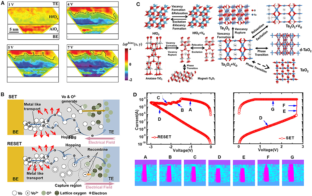
Figure 1. (A) The bias-induced phases featuring Δφbias(x,y) in the forming process of HfOx- resistive switching random access memory (RRAM). The intrinsic inner potential is removed by using the phase image of the pristine sample without bias. The dash curve is the boundary between the positive and negative phases. TE, top electrode; BE, bottom electrode. (B) Physical effects during SET and RESET processes. (C) Ab initio calculation results for various metal oxide materials such as HfO2, TiO2, and Ta2O5. (D) I–V curves and the corresponding CF evolutions simulated by the kinetic Monte Carlo method during RESET and SET processes. Reprinted from Kang et al. (2015), Huang et al. (2013), and Li et al. (2017).
To explain the physical origin of generation and rupture of the CF, multiple switching mechanisms have been proposed in recent years (Russo et al., 2007; Wei et al., 2008; Degraeve et al., 2010; Kwon et al., 2010; Goux et al., 2011; Kang et al., 2015). Combining with the experimental evidence, one widely accepted physical mechanism is the generation and combination of Vo with O2− (Gao et al., 2011; Guan et al., 2012; Huang et al., 2013; Kang et al., 2015). Based on the mechanism, the microscopic physical processes of switching of the typical TiN/HfOx/Pt device are shown in Figure 1B. In the SET process, O2− are ionized from the HfOx lattice accompanied by the generation of Vo. The O2− will be driven toward TE under the electric field and restored at the oxygen reservoir, which is the TiN electrode in the TiN/HfOx/Pt structure. The probability of above microscopic processes can be described as Guan et al. (2012):
where f is the vibration frequency of the oxygen atom, E0 denotes the average active energy of VO generation or O2− hopping, Δϕ is the barrier height reduction induced by the electric field, and T is the local temperature. In the RESET process, the electrons in the vicinity of Vo are depleted under the electric field, and then the positively charged Vo would recombine with the dissociated O2− released by the oxygen reservoir. The recombination of Vo and O2− finally results in the rupture of CF.
For other resistive switching materials, such as TiO2 and Ta2O5, the phase transition also takes place during the resistive switching (Wei et al., 2008; Kang et al., 2015). The phase transitions in TiO2 and Ta2O5 were calculated by ab initio calculations as shown in Figure 1C (Kang et al., 2015). In the Ta2O5-based RRAM, the phase transitions take place between Ta2O5 and TaO2, and Ta2O5 is semiconductive, while TaO2 is metallic. During the resistive switching, the CF is composed of both Vo and TaO2. Although the effects of Vo generation/recombination and phase transition coexist during switching, the Vo generation/recombination is the dominant effect based on the device simulation results (Zhao et al., 2016).
Based on the basic principle of Vo generation and recombination, the bipolar and unipolar switching characteristics can be explained by a unified model (Gao et al., 2011). Their physical origins of CF formation and rupture between the bipolar switching and unipolar switching are roughly similar. The difference is the location that stores and releases O2−. In the unipolar RRAM, the dissociated O2− would be absorbed or released by the easily reduced oxide clusters near the CF, and several different phases of oxide clusters coexist in the electrolyte material. The O2− will be thermally activated and recombine with the neighbor Vo in the RESET process. For both bipolar and unipolar RRAM, the electron transport in the CF is metallic, and the conductivity decreases with increasing temperature following the Arrhenius law (Ielmini et al., 2010). In the region with low Vo concentration, the electrons hop among the dispersive Vo, and the hopping rate can be calculated by the Mott hopping model (Mott and Davis, 1972). Therefore, the I–V characteristics are nonlinear for the HRS device as shown in Figure 1D. Based on the physical effects of resistive switching, the kinetic Monte Carlo simulations can be performed to investigate the switching dynamics in atomic scale. Figure 1D shows the CF evolution processes during RESET and SET processes (Huang et al., 2013). In the RESET process, the CF first ruptures at the interface between the TiN and HfOx layer, and then the gap region enlarges gradually. In the SET process, a thin CF first connects the electrode and residual CF, and then the thin CF would grow along the radius direction.
Even the filament effect and the correlated physical effects have been widely accepted for resistive switching, the direct experiment evidences of the physical effects in microscopic characterizations are still lacking. Future breakthroughs in atomic level characterization technologies may finally help people to clarify the underlying physical origins.
The RRAM characteristics can be improved or modified by inserting an assistant layer adjacent with the resistive switching layer, which composes a multifunctional electrolyte stack. A typical example is the Ta2O5/TaOX bilayer stack, which aims to improve the endurance characteristics (Wei et al., 2008; Lee et al., 2011). In the Ta2O5/TaOX stack, the oxygen-deficient TaOX layer, instead of TiN electrode in the HfOX-RRAM, acts as the oxygen reservoir. The generated O2− in the SET process would be absorbed by the TaOx layer, in which part of O2− will continue hopping in the TaOx layer under the electric field, while the rest will take the redox reaction with the oxygen-deficient TaOx and be stored as lattice oxygen. The oxygen concentration in the TaOx layer increases as O2− gradually oxidizes TaOx, leading to the resistance increase in the TaOx assistant layer. In this way, the current during the SET process can be adjusted dynamically and prevented from being too large. This can explain the self-compliance behavior observed in measured I–V characteristics in Ta2O5/TaOX-based RRAM as shown in Figure 2A (Zhao et al., 2016). Besides that, one remarkable characteristic of Ta2O5/TaOX-based RRAM is the superior endurance performance. The endurance can reach up to 1012 as shown in Figure 2A (Lee et al., 2011). Moreover, the endurance can be enhanced when choosing lower oxygen partial pressure during the deposition of TaOx. The enhanced endurance can be attributed to the capability of TaOx to take redox reactions with O2−, which can then be stored concentrated near CF in the TaOx layer. Figure 2A schematically shows the endurance model in the bi-layered TaOx-based RRAM (Zhao et al., 2015). During the resistive switching process, the concentrated distribution of absorbed oxygen guarantees the sufficient supply of O2− in each RESET cycle, otherwise, the O2− would distribute more dispersively in the oxygen reservoir. If the TaOx material is easy to take redox reactions with O2−, the endurance can be highly enhanced, otherwise the endurance behavior would be degraded.
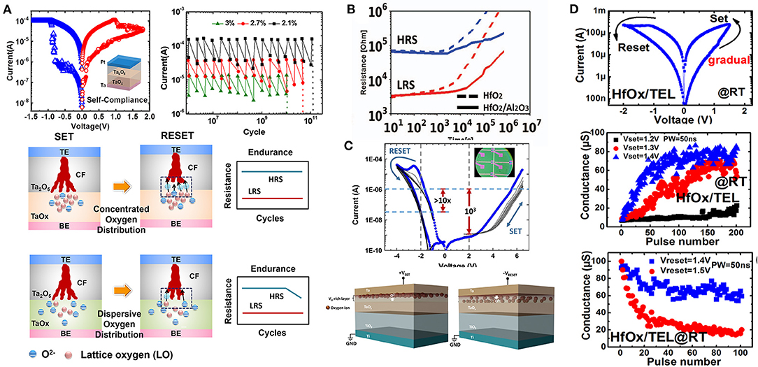
Figure 2. (A) The self-compliance and enhanced endurance characteristics of Ta2O5/TaOX-based RRAM and its schematic endurance model. (B) The retention characteristics at 200°C of the HfO2/Al2O3 device and its comparison with the single-layer HfO2 device. (C) Self-rectifying characteristics in the TaOx/TiO2-based RRAM with 103 rectifying ratio and the schematic mechanism. (D) Analog switching behavior under both SET and RESET pulses in the HfOx/TaOx RRAM. Reprinted from Lee et al. (2011), Azzaz et al. (2015), Chou et al. (2015), Zhao et al. (2015, 2016), Wu W. et al. (2017).
For HfOx-based RRAM, recent studies demonstrated that by introducing a thin Al2O3 layer into the HfO2-based RRAM devices, the switching uniformity, memory window, as well as the operating current can be improved compared with the single-layer HfOx RRAM (Yu et al., 2011; Goux et al., 2012; Azzaz et al., 2015). Figure 2B shows the LRS and HRS retention behaviors for the HfO2/Al2O3 device at 200°C. The comparison between the retention of HfO2 and HfO2/Al2O3 are also shown in Figure 2B. The insertion of the Al2O3 assistant layer greatly improves the device thermal stability. This can be explained by the increase in Vo diffusion barrier due to the incorporation of Al into the HfO2 matrix.
The assistant layer can also help the device realize self-rectifying property. Due to the sneak current issue in the RRAM crossbar array, the maximum array size is limited, which requires an additional selector to suppress the current crosstalk. One solution to reduce the cell area and fabrication complexity is to construct a RRAM device with highly non-linear I–V characteristics, which is also known as selector-less or self-rectifying. A Ta/TaOx/TiO2/Ti RRAM cell is constructed with a high self-rectifying ratio up to 103 for sneak current suppression (Chou et al., 2015). Figure 2C shows the I–V characteristics of the proposed device. No obvious SET transition is observed during the switching from HRS to LRS. Compared with a positive-bias current at 2 V, the device shows a three-order rectifying ratio at +2 V and −2 V. Different from the filamentary switching in a single-layer device, the switching mechanism in the TaOx/TiO2-based device can be attributed to the O2− migration under the electric field and the Schottky barrier modulation at the Ta/TaOx interface as shown in Figure 2C.
Compared with the abovementioned binary RRAM with two stable resistance states, the analog RRAM with hundreds of resistance levels is an attractive device to mimic the function of biological synapse for neuromorphic computing. A gradual resistance change requires analog modulation of CF evolutions, while it contrasts with the presence of the gap, as the current depends exponentially on the band offset and thickness of the gap. Another issue that contrasts the analog switching is the exponential dependence of physical effects on the field (Larcher et al., 2017). Mitigating the strong field dependence is the key to achieve analog switching, which can be achieved by introducing an assistant layer in the device. Several methods have been used to form the assistant layer such as introducing an AlOx layer in the HfOx-based RRAM (Woo et al., 2016a; Chuang et al., 2019), introducing a SiO2 layer at the TiN/TaOx interface (Wang et al., 2016), insertion of a TiO2 layer in the TaOx/Ti interface (Gao et al., 2015), and the Ar plasma treatment at the Ti/HfO2 interface (Ku et al., 2019). Figure 2D shows the analog switching behavior by introducing an oxygen-deficient TaOx layer in the HfOx/Ti RRAM cell at room temperature (Wu W. et al., 2017; Wu et al., 2018). For the HfOx/Ti RRAM cell, the experimental measurements indicate that when increasing the temperature in the HfOx layer, the abrupt switching changes to analog switching due to the thermal effect. Based on this principle, a thermal enhanced layer is designed with less thermal conductivity than metal, therefore it will confine the heat in the HfOx switching layer. In the HfOx/TaOx RRAM, the DC I–V characteristics exhibits gradual current change in both SET and RESET processes. For the operation scheme of identical pulses, the gradual conductance modulations are achieved in both SET and RESET processes as shown in Figure 2D. Besides the thermal effect, simulations also show that the slower diffusion of O2− in the bi-layer device would benefit the gradual resistance change (Larcher et al., 2017). The slower diffusion is due to the lower electric field within the oxygen reservoir layer, originated by the voltage distribution and the lower dielectric constant of the assistant layer compared with the resistive switching layer. Therefore, a careful thermal and electric design is required to achieve analog switching behavior.
For the analog RRAM, the distribution of multi-level resistance states is widely spread. The wide conductance distribution causes the overlap of neighboring conductance states, resulting in retention degradation (Huang et al., 2018). In addition, after programming the device to the target conductance state, the conductance of the device may experience a notable change in a short time scale, forming tail bits (Xu et al., 2020). This is called conductance relaxation effect, which is different from retention degradation. The relaxation effect and retention degradation are mainly due to the stochastic diffusion of O2− and Vo, thus can be suppressed by the restriction of O2− and Vo diffusion. For instance, Al doping in HfOx-based RRAM and HfO2/Al2O3 multilayer stack are used to suppress the Vo diffusion (Chen et al., 2013; Fantini et al., 2014). However, doping may introduce dopant variations with the device scaling down to a small size. A post annealing process after Hf/HfO2 RRAM formation was used to form an HfOx interface layer to enhance retention by slowing down the oxygen diffusion (Huang X. et al., 2016). Devices with worse state instability and retention need a short refresh interval to ensure accuracy of neural network, which brings extra power consumption.
The compact model is very important for the development of emerging devices. It can provide fast calculations of the device electrical properties and be implemented into standard IC design software to evaluate the performance of the target system. Moreover, a compact model involving the device physics can act as an interface between the device and the circuit. For RRAM device, based on the understanding on the microscopic properties of CF evolution and the correlated device characteristics, the physics-based compact models are investigated to capture the essential characteristics, which can be used to design and optimize the brain-inspired systems.
The first model of RRAM is the memristor model proposed by Chua (1971). Then a physical model for the device that behaves like a perfect memristor is proposed with a simplified explanation of current–voltage anomalies (Strukov et al., 2008). With the development of understanding of physical effects in RRAM, a compact model by considering the generation and recombination of Vo is proposed and implemented in Ngspice (Guan et al., 2012). Numerical compact models have also been developed based on the temperature and field-driven ion migrations (Larentis et al., 2012; Kim et al., 2013). By invloving the electro-themal effect, a physics-based compact model is proposed by bridging the switching behaviors with the evolution of CF configuration (Huang et al., 2013). The model is implemented into HSPICE and used for simulation of large-scale circuit by Verilog-A. In this section, this physics-based electro-thermal model will be discussed in detail.
Based on the kinetic Monte Carlo simulations in Figure 1D, the model with 3-D CF evolution process is developed as shown in Figure 3A (Huang et al., 2013). For the initial state of RESET, a cylindrical CF with the diameter w0 bridges two electrodes. The RESET process is modeled by the increase in gap distance x between the CF tip and the top electrode when the bias increases. The increase rate of x is expressed as dx/dt. The x determines the HRS resistance, and dx/dt determines the RESET speed. The dx/dt can be calculated by the slowest process among: (1) electrode releasing O2−, (2) O2− hopping in the switching layer, and (3) recombination between O2− and VO.
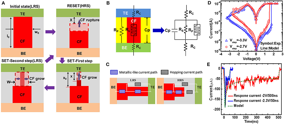
Figure 3. (A) Schematic of the conductive filament (CF) evolution model in the RESET and SET process. (B) Equivalent circuit with parasitic effects. (C) The low resistance state (LRS) and high resistance state (HRS) conduction model. (D) Measured and calculated DC and (E) AC characteristics for different operation schemes. Reprinted from Huang et al. (2013).
As an example, to illustrate the modeling process, we consider the O2− hopping process as the slowest process, which is also called the dominant process. During RESET, the amount of O2− flowing through the unit area of cross-section per unit time can be written as:
where is the O2− flow rate, a is the distance between two VO. The coefficient 1/2 is due to the two hopping directions of O2−. In dt, the amount of O2− hopping to VO is:
and the amount of VO that take recombination reaction with O2− is:
Combining Equations (3) and (4), we can get:
where Eh is the hopping barrier of O2−, E is the electric field, αh is the enhancement factor of the electric field for the lowering of Eh, and Z is the charge number of oxygen ion. If the O2− releasing or Vo recombination is the dominant process, the dx/dt can be calculated similarly.
For the SET process, the CF evolution is divided into two steps as shown in Figure 3A. First, a thin CF would grow from the residual CF and then connect to the electrode. Then, the thin CF would expand laterally along the radius direction. The reduction speed of gap distance dx/dt and the increase in speed of CF radius dw/dt can be calculated similarly, which are the two factors that influence the SET operation. The equivalent circuit of RRAM is shown in Figure 3B. It consists of a parallel capacitance (Cp), a parallel resistance (Rp), contact resistance (Rc), and the resistive switching elements (Rs). The conduction of the switching element can be modeled with metallic conduction in the CF region and hopping conduction in the gap region as shown in Figure 3C (Huang et al., 2013). The temperature also plays a very important role in resistive switching. In the model, we assume uniform temperature in the electrolyte layer, and the temperature at LRS can be written as Russo et al. (2009):
where T0 is the environment temperature, Rth is the effective thermal resistance of the electrolyte. Involving the model of conduction and temperature, the I–V characteristics can be calculated.
The calculated DC and AC electrical characteristics are shown in Figures 3D,E. The compact model can accurately reproduce the gradual RESET and the abrupt SET in the DC I–V characteristics. The transient response current waveforms for different RESET programming schemes of −2 V/500 ns and −2.3 V/50 ns can also be successfully reproduced. The excellent agreement between the modeling and measured results shows the validity and universality of this compact model to capture the main features of the RRAM devices. Using the model, the critical parameters during switching can be extracted from the physical view, thus providing design space for device optimization and device–circuit co-design.
Besides the basic resistive switching characteristics, the compact model for synaptic features of HfOx-based RRAM is developed to satisfy the co-design requirements of RRAM synapses and the CMOS neurons in the neuromorphic computing systems (Huang et al., 2017). The conductance change in HfOx-based RRAM can emulate the activating or deactivating ion channels of biological synapse, and the gradual RESET and stochastic SET can emulate the biological depression and potentiation processes. During RESET process, multiple intermediate states can be achieved under proper spike pulses, and they can be divided into three stages as shown in Figure 4A (Huang et al., 2017). Figure 4B schematically shows the model of gradual RESET with three stages. In the first stage, with O2− released by the electrode, the Vo density near the electrode would decrease, resulting in the slimming of CF. The conductance in this stage is linear with CF width, so the conductance decrease is relatively low. In the second stage, CF is ruptured from the tip, and the O2− released by the electrode would continue recombining with VO in the CF. In this stage, the resistance is approximately exponentially dependent on the gap distance, and thus, the conductance decreases fast. In the third stage, due to the decrease in electric field in the gap, the reaction rates of O2− hopping and Vo recombination decreases; hence, the resistance would tend to saturate.
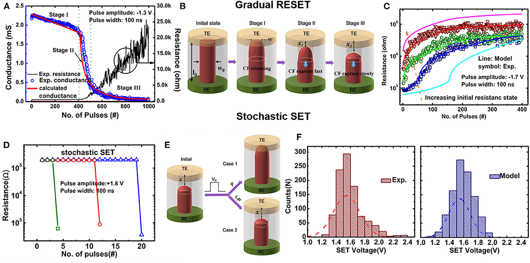
Figure 4. (A) Measured gradual RESET under consecutive identical pulses. (B) CF evolution model of gradual RESET. (C) Measured and calculated gradual RESET with different initial states. (D) Measured binary stochastic SET under consecutive identical pulses. (E) Model for stochastic SET. (F) Measured and calculated SET voltage distributions in 1,000 cycles. Reprinted from Huang et al. (2017).
The SET process in the single-layer HfOx-based RRAM is typically abrupt; thus, only binary states can be achieved. The SET also demonstrates the stochastic transition behavior as shown in Figure 4D. Figure 4E shows the model of stochastic SET. The device will be switched to LRS with the probability P after a positive pulse, which is related with the pulse amplitude V and pulse width Tw. The probability P can be written as:
P follows a distribution even for the same device.
The proposed model is verified with measurement data as shown in Figure 4C. The gradual resistance modulation under consecutive identical pulses can be well-reproduced. The figure indicates that more intermediate states can be achieved with lower initial LRS, which is beneficial for synapse application. Figure 4F shows the measured and calculated SET voltage distributions in 1,000 cycles for the same device. They both roughly follow a normal distribution with similar mean value and standard variation. Good agreements between measurements and calculations demonstrate the validity of the model to capture the RRAM synaptic features. In addition, the SET stochasticity can be employed to generate stochastic numbers, which demonstrates great potential in the application of stochastic computing. This will be further discussed in the Stochastic Computing section.
As discussed in the Device Optimization With Multifunctional Assistant Layer section, analog RRAM devices have been realized by introducing an assistant layer. Many efforts have been made to mitigate the non-ideal effects of analog RRAM including the programming non-linearity and asymmetry, variability, and tuning voltage sensitivity (Woo et al., 2016a; Wu W. et al., 2017; Wu et al., 2018). Compact models for analog RRAM have been developed to provide insights into the influence of electrical and thermal effects of assistant layer on the device characteristics and provide guidance for the optimization of non-ideal effects. In addition, the compact models can provide fast and accurate evaluation of the training accuracy. Multiple theories have been used to explain the analog switching behavior. One is the multiple-weak-filament theory, in which the local Vo concentration in the CF region is lower than the binary RRAM; thus, multiple weak CFs are assumed to be formed due to the percolation effect (Liao et al., 2020). The number of weak CFs and their conductivity are strongly dependent on the Vo concentration. Another theory describes CF with one resistive switching (RS) region and one Vo-rich (VR) region (Cai et al., 2020). The Vo concentration varies in the RS region during resistive switching processes, thus, leading to the gradual resistance modulation. Based on above theories, the key factor for analog properties is to control the Vo concentration and distribution in the CF, and the Vo modulation in multiple weak CFs can be treated as the Vo density redistribution in the RS region. The compact model with Vo modulation in the RS region will be introduced in detail in the following part.
In the model, the CF is modeled with the RS region and one VR region as shown in Figure 5A. In the SET process, due to the generation of Vo, the percentage of Vo in the RS region (ΔCV+) increases, which can be described as:
where CV is the Vo concentration. For RESET process, the Vo recombination leads to the decrease in CV. Besides the kinetic barrier Eo, the releasing of O2− also relies on CV at the interface of CF and the intermediate modulation layer (IML). The O2− percentage in the RS region CO is changed by the released O2−, which can be described as:
The reduced percentage of Vo in the RS region is expressed as:
where Er is the recombination barrier. The conduction of the analog RRAM is modeled in Figure 5B. In the RS region, the effective conductivity can be calculated based on the effective medium theory, while the conductivity of IML can be calculated by evolving the O2− concentration in IML. Based on above model, the I–V characteristics of the analog RRAM can be calculated as shown in Figure 5C. Gradual SET and RESET behavior can be well-reproduced by the model, which is in good accordance with measurement data obtained from the TiN/TaOx/HfOx/TiN device in Wu et al. (2018). Based on the model, the continuous conductance accumulation can be reproduced under identical pulses as shown in Figure 5D. By adjusting the resistivity ρ of IML, the compact model shows good agreement with experiments about the linearity improvement. The non-linearity of conductance is influenced by both the electrical and thermal effects of IML. The impacts of electrical and thermal effects of IML on potentiation and depression are investigated as shown in Figures 5E,F. The results indicate that reduced thermal conductivity κ enlarges the tuning window due to the acceleration of Vo generation under high temperature, and the switching window is reduced with increased resistivity ρ. Increasing ρ and κ of IML both improve the linearity of conductance tuning, but the impact of resistivity is more obvious. Therefore, IML material with high resistivity would be more recommended to improve the linearity for learning accuracy in the application of neuromorphic computing.
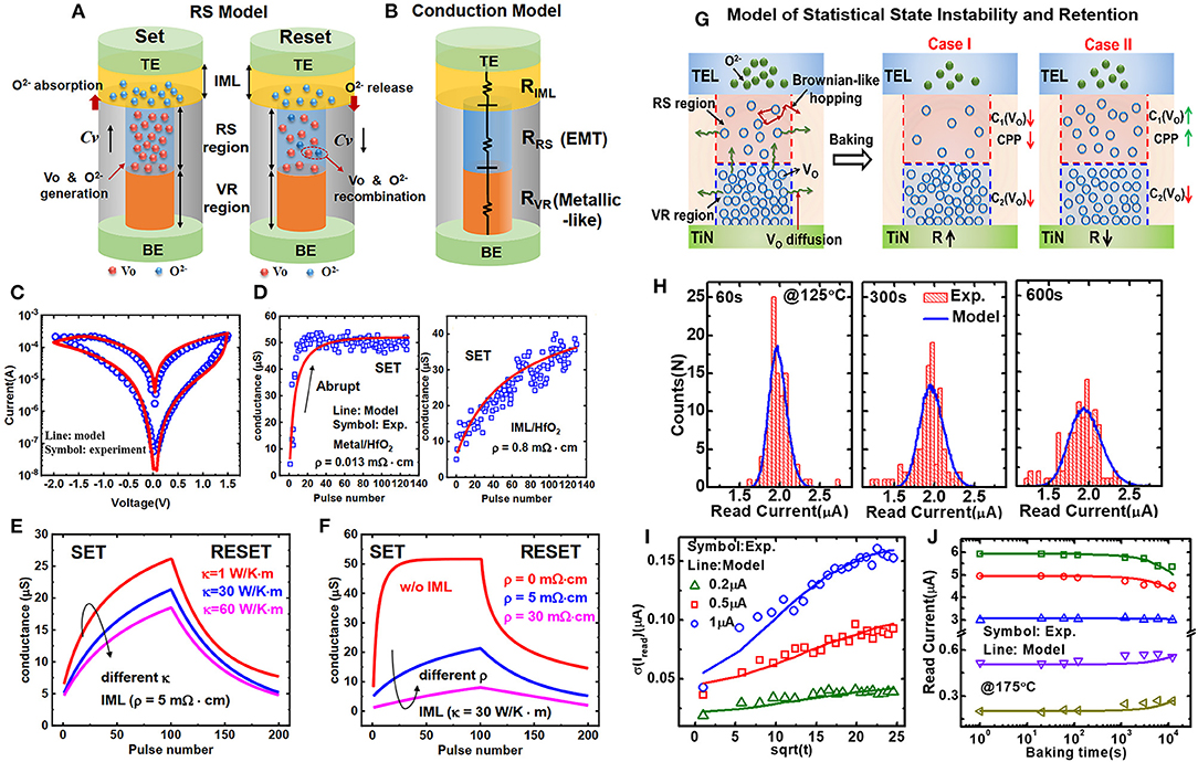
Figure 5. (A) The physical switching model of the analog RRAM. (B) The conduction model. (C) The measured and calculated I–V characteristics. (D) The comparison between abrupt and gradual SET by introducing an intermediate modulation layer (IML). (E) The influence of thermal conductivity and (F) resistivity on the analog switching behavior. (G) Physical model of state instability and retention degradation. (H) Measured and calculated evolution of read current distributions. (I) Measured and calculated standard deviation of read current vs baking time. (J) Measured and calculated retention degradation for a long baking time at 175°C. Reprinted from Cai et al. (2020) and Huang et al. (2018).
Although analog RRAM shows great potential in weight storage and weight updating, it suffers from serious state instability and retention degradation issues, which greatly affect the performance of neural network. A physics-based analytic model is developed to describe the statistical state instability and retention behaviors of analog RRAM (Huang et al., 2018). In the model, the diffusion of Vo, the Brownian-like hopping of Vo during diffusion, and the recombination of Vo are considered. Figure 5G shows the physical model of the state instability and retention degradation. In a relatively short time, the Vo hopping is similar to the random Brownian movement. The Brownian-like hopping of Vo at the critical site of the current percolation path (CPP) results in the fluctuation of conductance, which is also called as the state instability. In a relatively long time, Vo diffuses along the radius direction and recombines with the O2− released by the IML, thus the Vo concentration C(Vo) in the RS/VR region and the corresponding conductance decrease (case I). The diffusion of Vo from the VR region to the RS region will increase the conductance because the cell resistance mainly depends on the C(Vo) in the RS region (case II). To sum up, the diffusion and recombination of Vo will result in the retention degradation. C(Vo) in the RS and VR regions are the key parameters to characterize the state instability and retention degradation. The mean C(Vo) can be obtained as a function of time by calculating the diffusion and recombination of Vo. Figure 5H shows the measured and calculated read current distribution at different baking times. The distribution becomes wide with time. The mean and standard deviation of the read current are in good accordance with the measured data. The measured and calculated standard deviations of the read current at different states are shown in Figure 5I, which indicates that the model can reproduce the statistical state instability. To further verify the model, the 1-kb analog RRAM array is measured under higher temperature and longer time. Figure 5J shows the retention behavior under 175°C of 1.2 × 10⁴s, which agrees well with the model prediction. The results indicate that the mean read current of high current states decrease with time, while the mean read current of low current states increase with time. The model can be used to evaluate and optimize the performance neural network. Optimized synapse structures and refresh operation schemes can be proposed under the guidance of the model to mitigate the performance degradation, which can significantly enhance the reliability of the RRAM-based neural network.
In the era of big data, the amount of data is explosively growing every day especially the non-structured data such as pattern, voice, and video. However, due to the von Neumann bottleneck, the traditional computing paradigm has a hard time in handling the task of a large amount of non-structured data. Fortunately, in recent years, brain-inspired computing has developed rapidly and has demonstrated great advantages in the fields of recognition and information processing, which could supplement the shortcoming of the traditional computing. In this section, the specific applications of RRAM-based brain-inspired computing including neuromorphic computing, computing in memory, and stochastic computing will be introduced.
Neuromorphic computing is a kind of computing paradigm for accelerating neural networks used in data-centric computing, which paves the way for artificial intelligence with low power consumptions, mimicking the synapse- and neuron-interconnected biosystems in the human brain. RRAM is widely regarded as one of the promising candidates of artificial synaptic device, and its crossbar structure can be utilized for the hardware acceleration of the neural networks (Hochreiter and Schmidhuber, 1997; Hinton et al., 2006; Russo et al., 2009; Krizhevsky et al., 2012; Graves et al., 2013; Silver et al., 2016). The Vo/ion-based mechanism of RRAM controlling the device conductance can emulate the synaptic plasticity, acting as the base for learning and memory operations of the brain. RRAM enables high-precision synaptic weight over 6 bits, bidirectional conductance modulation, and tiny weight accumulation, so that a high-performance deep neural network algorithm could be realized; besides, RRAM could also implement the basic functions of biological synaptic, such as spike time-/rate-dependent plasticity (STDP/SRDP) and paired-pulse facilitation (PPF), which provides an approach to establish spike neural networks (SNN) (Yu et al., 2012; Gao et al., 2014, 2016; Prezioso et al., 2015; Wang et al., 2017).
In a neural network composed of neurons and synapses, neurons are connected by synapses with different weights. A two-layer neural network can be directly mapped to a RRAM crossbar array, where WLs are connected to the pre-neurons, and BLs are connected to the post-neurons as shown in Figure 6A. Through the RRAM-based synapse, the signals sent by the pre-neurons can be transmitted to the post-neurons. The synapse weights are mapped to the RRAM conductance. The output current Ij at the jth column can be written as:
where Vi is the voltage applied to the ith row, and Gi, j is the conductance of RRAM at row i and column j. Therefore, the weighted sum, which is a time- and energy-consuming step for neuromorphic computing based on conventional computing system, can be performed by the RRAM crossbar array in one step. Generally, the integrated current at each column will be converted to voltage pulse by the neuron circuit and sent to the post-neuron.
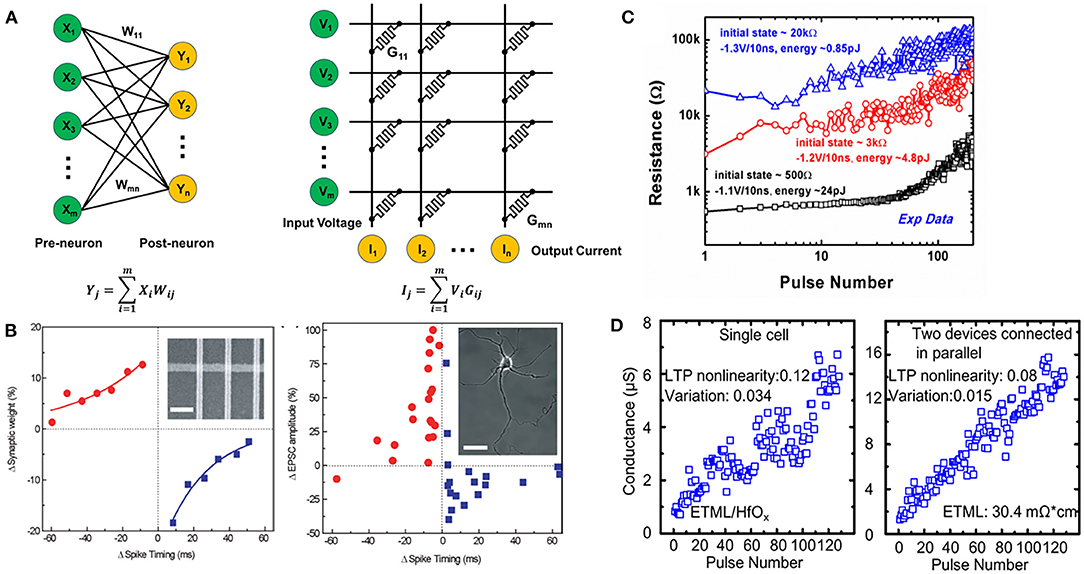
Figure 6. (A) Schematic of the RRAM-based neural network. (B) Demonstration of the spike time-/rate-dependent plasticity (STDP) in the RRAM-based synapse and the excitatory postsynaptic current of rat hippocampal neurons. (C) Measured gradual training process of RRAM under consecutive identical pulses. (D) Improved linearity of conductance tuning in RRAM synaptic devices by introducing an electro-thermal modulation layer. Reprinted from Wu et al. (2018), Yu et al. (2012), and Jo et al. (2010).
The weights of the RRAM-based synapses can be updated in two ways. The first way is based on the working mechanism of the biological neural networks, in which the weight can be updated based on certain modification rules, such as the STDP (Jo et al., 2010; He et al., 2014; Du et al., 2015; Eryilmaz et al., 2015; Prezioso et al., 2016). For an STDP synapse, the weight update direction depends on the time difference Δt of the spikes from the pre-neuron and post-neuron as shown in Figure 6B (Jo et al., 2010). When spikes from the pre-neuron are before (or after) the post-neuron, the synaptic weight increases (or decreases). It can be found that the relation between the change in the synaptic weight and Δt can be well-fitted with exponential decay functions, which is similar to the STDP characteristics of biological synaptic systems as shown in Figure 6B. Arbitrary STDP behaviors, such as anti-STDP, symmetric STDP, and STDP with sin decay function can be achieved with this feature. In addition to STDP, several other synaptic functions have been realized by RRAMs, such as SRDP, short-term plasticity (STP), and long-term plasticity (LTP) (Yu et al., 2012; Gao et al., 2014, 2016; Prezioso et al., 2015; Wang et al., 2017). All these achievements are helpful to the researcher of biological neural network and will significantly enhance the intelligence of neuromorphic hardware. Although various functions of biological synapse have been realized by the RRAM, a large neural network based on such synapse update rule is still lacking due to the fact that the working mechanism of the brain is not clear. Moreover, for the SNN, the training is mainly achieved using the biology-like unsupervised learning rules, which makes it difficult to support complex practical cognitive applications.
Another principle to update the weight is the backpropagation (BP) learning rule, which has shown its advance in pattern and speech recognitions. The HfOx-based RRAM synaptic device has been demonstrated with sub-pJ energy per spike to build a neuromorphic visual system. The measured gradual training process of RRAM under consecutive identical pulses are shown in Figure 6C (Yu et al., 2012). According to the BP algorithm, the desirable characteristic of the RRAM synapse is multilevel (states > 64) and low power (<0.1 pJ/spiking) switching, and the linear and symmetric responses of synapses to electric pulses are required for the training process. However, that is a quite difficult task for RRAM-based synapse. To modulate the characteristics of the RRAM-based synaptic device, the optimization of linearity and symmetry of conductance modulation is essential to realize efficient training tasks. The programming schemes can be optimized by varying the operation voltage, pulse width, gate voltage in 1T1R structure, and compliance current (Wu et al., 2012; Park et al., 2013; Woo et al., 2016b; Ku et al., 2019). However, this method brings additional circuit overhead and power consumption. Then a more favorable solution was proposed to optimize an identical programming scheme independent of device conductance states, and the abrupt resistance change can be avoided (Woo et al., 2016b). Besides the operation scheme, the non-linearity can be mitigated by the device engineering. As has been discussed in the Device Optimization With Multifunctional Assistant Layer section and the Analog Resistive Switching Random Access Memory section, an electro-thermal modulation layer has been inserted between the top electrode and resistive layer to control the distribution of electric field and temperature in the filament region; the linearity of conductance tuning is improved as shown in Figure 6D (Wu et al., 2018). However, the dynamic range decreases by this method.
The multilevel conductance capability of the RRAM-based synapse can impact the inference accuracy. Figure 7A shows the impact of weight precision on the accuracy of a two-layer fully-connected neural network for MNIST dataset (Chen et al., 2017). At least six bits are required for online training, and one or two bits are sufficient for offline classification. Higher weight precision is required for complicated convolutional neural network as shown in Figure 7B (Yang and Sze, 2019). To meet this requirement, a large ON/OFF ratio with multiple intermediate resistance states is essential. Regarding the issue of non-ideal device characteristics, other possible solutions may be from the interaction and optimization between devices and algorithms or architectures. For example, in the incorporation with recently proposed binarized neural networks (BNNs) based on modified BP algorithm, the impact of non-linearity in RRAM-based synapses on system performance can be effectively eliminated. A new BNN-based hardware implementation approach to utilize the non-linear synaptic cells to achieve highly efficient online training is shown in Figure 7C (Zhou et al., 2018). Based on the presented implementation approach, the conductance tuning non-linearity has little impact on the recognition accuracy of neural network. However, the binarization of weight would lead to the information loss, and the discontinuity of its quantization function increases the difficulty of the optimization of neural networks (Qin et al., 2020).
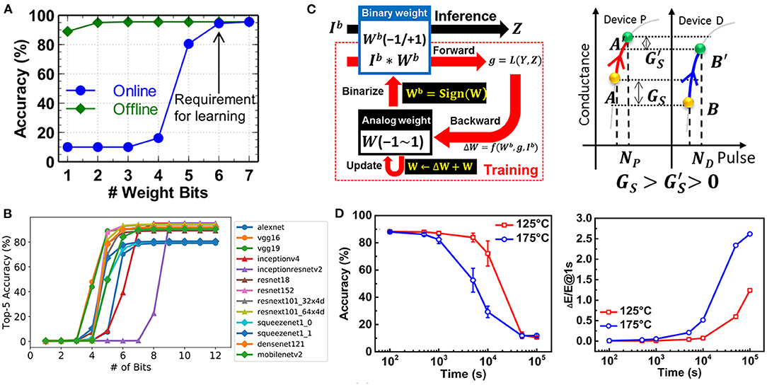
Figure 7. (A) Impact of weight precision on accuracy in a two-layer fully neural network for MNIST dataset. (B) Impact of weight precision on accuracy of representative DNNs. (C) Schematic of binarized neural network (BNN) algorithm and the typical example of weight accumulation process. (D) Recognition accuracy and normalized energy consumption change as a function of baking time. Reprinted from Chen et al. (2017), Yang and Sze (2019), Zhou et al. (2018), and Xiang et al. (2019).
The robustness of RRAM-based neural network is related with the reliability of the RRAM-based synapse such as retention, endurance, and immunity to noise. The impacts of device state instability and retention on the performance of DNN was investigated (Xiang et al., 2019). Using the analytic model for RRAM state instability and retention degradation in the Analog Resistive Switching Random Access Memory section, the performance of the 11-layer RRAM-based DNN for CIFAR-10 recognition can be evaluated. Figure 7D shows the dependence of the recognition accuracy on the baking time at 125 and 175°C. The accuracy decreases remarkably with time due to the overlap among neighboring resistance levels. Meanwhile, the energy consumption during the inference increases with time as shown in Figure 7D. This is because, for the proposed neural network, more than 90% of the weight is located near 0, which means most of the RRAMs are in the low conductance states. More importantly, the differential pairs are used to store weight, and one device is in the conductance state at least. Therefore, the conductance of a large proportion of RRAMs increases with the baking time, which dominates the energy consumption. To enhance the reliability of DNN, both the device characteristics and the operation scheme should be optimized.
To design and optimize the RRAM-based neuromorphic system, modeling platforms have been developed to design the neuromorphic computing circuits and find the algorithmic constraints with device properties (Chen et al., 2017; Larcher et al., 2017; Haensch, 2018). A comprehensive model for SNN based on STDP is developed to predict the learning efficiency and time for unsupervised learning from detailed spice-like models to high-level analytical compact models (Pedretti et al., 2017). The analytic model includes all possible pattern/noise and noise/pattern sequences of input spikes as driving forces for potentiation and depression, and can predict the time evolution of pattern weight and noise weight for any set of input variables. Using the model, the impacts of noise density, pattern density, and pattern/noise probabilities on learning efficiency can be investigated, and a learning efficiency improvement up to 92% can be realized by using optimized noise in unsupervised learning of handwritten digits from the MNIST database. In terms of system-level learning accuracy and hardware performance metrics, an integrated device-to-algorithm framework NeuroSim+ for benchmarking synaptic devices and array architectures was developed (Chen et al., 2017). The framework includes the technology and memory models in the device level, the synaptic array architectures and neuron periphery in the circuit level, and the neural network topologies in the algorithm level. The impact of device non-ideal properties on learning accuracy, the area, latency and energy estimation in the circuit level can then be investigated by this framework. A two-layer multilayer perceptron (MLP) neural network with MNIST handwritten digits is adopted as the training and testing dataset to implement online learning and offline classification. In the MLP neural network, the MNIST input images are converted to black and white data to reduce the encoding complexity. The weights are mapped to the synaptic cores, which are the computation units for performing weighted sum and weight update. The synaptic core can be categorized into the binary RRAM and analog RRAM, where binary type is more mature. When a weighted sum or weight update instruction is given during feed forward and BP, the instruction will be sent to the RRAM array and device behavior model for calculating the computation error and sent to NeuroSim to evaluate the circuit performance. The framework facilitates the design space exploration from device to algorithm, which is helpful to benchmark different synaptic device candidates and array architectures for neuromorphic applications.
For RRAM-based neuromorphic computing, although some small-scale neural networks have been demonstrated, it is still far from being applied. The challenges come from the design and fabrication of RRAM arrays with high performances, device characteristic engineering, neuron circuit design, and algorithm modification. Possible solutions should consider the interaction and optimization between devices and algorithm or architectures.
The conventional computation systems process information and store information separately, which brings huge energy cost and time wasting in data transfer between the computing units and memories. In order to break the von Neumann bottleneck in both the device and architecture level and meet the requirement for energy-efficient information system, the RRAM-based logic is proposed as a promising solution, which can perform logic operation and store the output in the same physical location (Borghetti et al., 2010; Li et al., 2015a; Huang P. et al., 2016).
In 2010, the RRAM-based stateful logic operation was first proposed and experimentally demonstrated (Borghetti et al., 2010). The basic logic operation is the implication (IMP), and the operation is based on two RRAM devices (P and Q) and one resistor as shown in Figure 8A. The resistance state stored in P and Q represents the logical value. IMP is performed by two simultaneous pulses applied on P and Q to execute conditional toggling on Q depending on the state of P and Q. The output of the operation is then stored in Q. If we define HRS as “1” and LRS as “0,” the IMP result is summarized in Figure 8A. Based on this principle, other logic computations can also be performed. However, the initial state of Q is covered during the operation, which hinders the logic cascading, and the Q needs a copy operation if the value is used more than once (Li et al., 2015b).
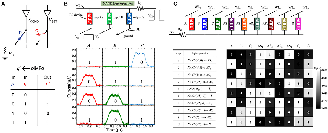
Figure 8. (A) RRAM-based IMP logic operation and the truth table. (B) The subcircuit of the NAND operation by using three RRAM devices with common WL and the corresponding measured results. The logic inputs are stored in devices A and B, while Y stores the output. (C) The subcircuit of one-bit full adder and the corresponding computation procedure. Here “NAND(A, B) → Y” represents that states of devices A and B are executed; the NAND operation and the output are stored into device Y. Reprinted from Borghetti et al. (2010) and Huang P. et al. (2016).
To prevent the input value from being covered, a method to execute NAND and logic operations in one step was proposed (Huang P. et al., 2016). The subcircuit to realize a NAND operation is shown in Figure 8B. In the circuit, the device top electrodes are connected to a common WL. A strong pulse is applied to the WL via a reference resistor, and a small pulse is applied to devices A and B through BL. For device Y, the BL is grounded. The input for the operation is the resistance states of A and B, and the output will be stored in Y, whose initial state has been switched to HRS. If A and B are both “1,” the potential of common WL is close to VDD, then Y will be programmed to “0” after the operation. If any input device is “0,” the potential of common WL is close to VR; thus, the output Y will still be “1.” By this way, the NAND logic operation is performed. The value of VR, VDD, and RG should be carefully designed to guarantee the NAND operation. VDD should be larger than the SET voltage in order to compensate the voltage drop across RG. As for VR, on one side, it should be large enough to avoid the switching of A and B; on the other side, it should be small enough to avoid the switching of Y. The experimental demonstration of the NAND logic is shown in Figure 8B. The logic function of the subcircuit can be reconfigured by changing the applied voltage. For example, the AND logic can also be realized using the same subcircuit by exchanging the VDD and VR.
Besides the basic logic operation, compound logic operation can be executed with latching the NAND logic operation. Figure 8C shows an example of a full adder. The subcircuit is composed of nine RRAM devices including three input devices (addend A, summand B, and carry-in Ci), two output devices (summary S and carry-out Co), and four assisted devices (AS1-AS4). The computation procedure is shown in Figure 8C, which needs 10 sequential steps. The corresponding logical states after each procedure are read out and demonstrated as gray-scale maps. The measured data indicate that the function of a full adder can be realized correctly. In order to realize the logic operation in arbitrary positions in the RRAM array, the structure of devices with the same BL was also proposed and verified (Huang P. et al., 2016). The same computing task can be performed parallelly by cells in different rows or columns in the RRAM array by simultaneously applying the pulses to the corresponding ports of BL and WL.
One challenge for the RRAM-based stateful logic is the device variations, which may cause errors to the logic operation. Therefore, the logic operation should be robust to these device variations, which include the SET voltage variation and resistance variation. To quantitatively describe the robustness of the logic operation, the dependence of maximum tolerance to SET voltage variation on the resistance window (RH/RL) was investigated by HSPICE simulation (Shen et al., 2019). The results indicate that compared with the conventional scheme based on 1R structure, the dual gate voltage scheme in the 1T1R array shows higher robustness to the SET voltage variations as RH/RL changes from 25 to 10,000. The variation of resistance in HRS and LRS will reduce the effective resistance window. For each given SET voltage variation, there exists a tolerable resistance window to ensure the successful logic operation.
The Boolean logic computing is closer to the off-the-shelf system compared with the neuromorphic computing paradigm, which does not require new algorithm or software. However, the development of the RRAM-based in-memory logic is very slow due to the lack of application scenarios, and the demonstration of complete computing and memory unit is still missing.
Stochastic computing (SC) is a highly fault-tolerant and energy-efficient computing paradigm, which can realize complex functions with simple logic units (Gaines, 1969; Lv and Wang, 2017; Hu et al., 2019). Different from the traditional binary computing, SC operates on stochastic bit streams (SBSs), which emulate the neural spikes processed by the brain in the form of long sequences of noisy voltage spikes as shown in Figure 9A. The information contained in the SBS is the frequency at which the spikes appear randomly within a period of time. For example, the value 0.4 can be represented by a 10-bit SBS {1,0,0,1,0,1,0,0,1,0}, where the probability of “1” is 0.4. The position of “1”s in the SBS is random, so different SBSs can represent the same value. Moreover, SC can be implemented with simple arithmetic units. For example, A multiplied by B can be operated with an AND gate, while A plus B can be operated with a MUX (Lv and Wang, 2017; Yang et al., 2017; Hu et al., 2019). Compared with the binary system, the SBS is more fault tolerant because one-bit flip is almost negligible. Therefore, SC can be used in highly fault-tolerant applications such as parity-check decoding, image processing, filter design, and neural networks (Gaudet and Rapley, 2003; Ma et al., 2012; Alaghi et al., 2013; Li P. et al., 2014; Canals et al., 2016; Li B. et al., 2016; Li Z. et al., 2016).
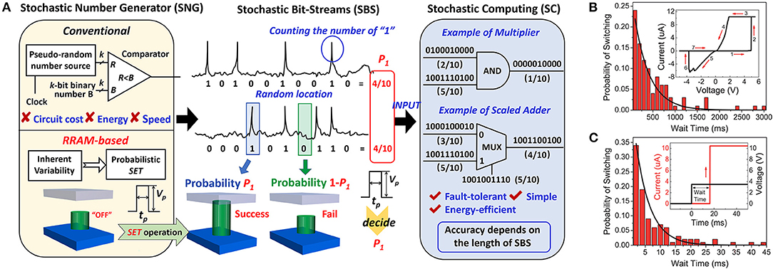
Figure 9. (A) The schematic of the RRAM-based stochastic number generator (SNG) in the stochastic computing (SC) system. The RRAM-based SNG utilizes the probabilistic SET to randomly generate “1” or “0.” (B) The SET waiting time distribution when the pulse amplitude is 2.5 V and (C) 3.5 V. Reprinted from Knag et al. (2014) and Zhao et al. (2019).
The biggest challenge to realize SC is to generate SBS efficiently. The traditional stochastic number generator (SNG) is composed of a pseudo stochastic number-generating unit such as the linear feedback shift register and a comparator. Compared with the simple computation unit of SC, the CMOS-based SNG occupies up to 80% of the system circuit area, which brings huge hardware overhead. RRAM devices, with the feature of inherent variability, shows great potential to be used as low-cost and energy-efficient SNG (Gaba et al., 2013; Suri et al., 2013; Knag et al., 2014; Moons and Verhelst, 2014; Ielmini and Wong, 2018; Wang et al., 2018; Carboni and Ielmini, 2019; Zhao et al., 2019). The inherent variability of RRAM originates from the probabilistic SET process as have been discussed in the Binary Resistive Switching Random Access Memory section (Figure 4). Figures 9B,C are the measurement results of the waiting time distribution during the SET process (Knag et al., 2014). The SET waiting time can be obtained by performing continuous RESET and SET operations on the device and then recording the time before the transition from HRS to LRS during each SET operation. Based on the measurements, the SET waiting time roughly follows the Poisson distribution, and the distribution curve will shift left or right when changing the pulse amplitude. Therefore, when consecutively applying SET and RESET pulses on the device, whether the CF would be generated inside the device is random, so a sequence of different current levels can be obtained, as shown in Figure 10A. Using “1” representing the LRS and “0” representing HRS, an SBS of n bits can be achieved. The SET probability is determined by the intensity of SET pulse; thus, by adjusting the pulse amplitude and pulse width, the numerical value represented by the SBS can be adjusted.
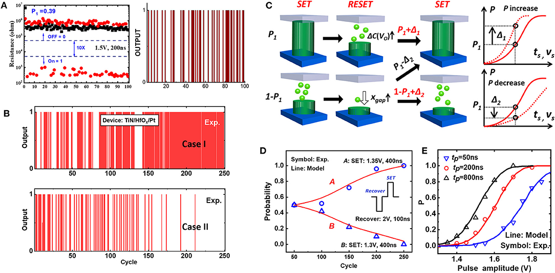
Figure 10. (A) The measured resistance state after 100 consecutive SET and RESET pulses and the corresponding SBS. (B) The measured SBS with probability shift behavior between continuous cycles with the same initial probability. (C) The model of probability shift behavior. (D) The measured and calculated SET probability shift behavior. (E) The measured and calculated SET probability curve with different pulse intensity under optimized operation scheme. Reprinted from Zhao et al. (2019).
To accurately control and predict the SET probability, the probability should be quantitatively modeled considering the device physics, as a small deviation of the input signal could affect the probability significantly. By considering multiple variation sources including the atom thermal vibration, manufacturing parameter variation, and cycle–cycle gap distance fluctuation, the behavior of the RRAM-based SNG can be modeled (Zhao et al., 2019). However, the RRAM SET probability may shift upward or downward between continuous cycles. Figure 10B shows the measured SBS with probability shift behavior of TiN/HfO2/Pt device. The unstable SET probability will influence the accuracy of the SBS, which must be mitigated for the application of RRAM-based SC. The probability shift behavior is modeled as shown in Figure 10C. Due to the different SET results in the N−1th cycle, the SET probability between the N−1th and the Nth cycles will increase or decrease. For example, the upper figure in Figure 10C corresponds to the situation where the CF successfully connected the electrodes during the N−1th SET process, and the device represents “1” after this operation. At this time, the concentration of the remaining Vo increases after RESET. The probability of generating “1” in the next SET operation increases, and the corresponding SET probability distribution curve would shift left. The model can well-reproduce the probability shift behavior observed in experiments as shown in Figure 10D. The increase or decrease of SET probability with cycles is due to the mismatch between SET and RESET pulses; thus, an optimized operation scheme is proposed by the model to suppress the probability shift behavior by applying an additional deterministic SET before each RESET operation. After suppressing the probability shift behavior, the SET probability dependence on pulse amplitude and pulse width can be investigated. Figure 10E shows the calculated and measured SET probability curve with different pulse strengths. The SET probability changes with pulse strength; thus, one can use this curve to obtain the device operation scheme depending on the desired probability, which is the value represented by SBS in the SC application.
In addition to the SET operation, the RESET operation also has a great influence on the SET probability. When increasing the amplitude of RESET pulse, the probability distribution curve shifts to the right. This is because a stronger RESET pulse will increase the gap length before each SET, which will reduce the probability of a successful SET. Therefore, to obtain the expected SET probability in a RRAM-based SNG, the SET and RESET operations should be both carefully designed. Moreover, due to the randomness of resistive switching and the noise in the pulse signal, the length of SBS should be properly selected to avoid a large error. The accuracy of SBS can be improved by using longer SBS, but the energy consumption and calculation time will also increase exponentially (Gaines, 1969). Therefore, according to the requirements of the SC application scenarios, the accuracy, energy consumption, and calculation time should be collaboratively designed.
The challenge facing the RRAM-based SC is the uncontrollable device stochasticity, so the distribution and probability of switching cannot be accurately predicted, which would seriously affect the accuracy of SC. Although the improvement of accuracy can be realized by using a longer bit stream length, the energy consumption will be greatly increased, resulting in the design trade-off between accuracy and energy consumption. The cost-effective design techniques that minimize the disadvantages such as low precision and long bit-streams are highly required.
The RRAM-based brain-inspired computing systems has achieved remarkable progresses in the past decades. Various computing paradigms have been proposed to exploit the device physics to perform neuromorphic computing, in-memory logic, and stochastic computing. However, some key issues still need to be addressed such as the device variability, forming voltage, selector device, and non-linearity/symmetry of RRAM-based synapses; thus, the design and optimization of structures, materials, and operation schemes in the device level, by means of the deeply physical understanding and innovative device-engineering methods, are still required. Moreover, the corresponding architectures and algorithms that can be utilized to construct power-efficient brain-inspired computing systems are still being developed, and it highly desires the persistent and creative research to the interaction and optimization between devices and algorithms or architectures.
YZ and RC contributed to the writing of the manuscript. RC and JK revised the manuscript. PH and JK helped with the supervision of the study. All authors contributed to the article and approved the submitted version.
This work was supported, in part, by the National Key Research and Development (2018YFE0100800), National Natural Science Foundation of China (61841404 and 62004005), and the 111 project (B18001).
The authors declare that the research was conducted in the absence of any commercial or financial relationships that could be construed as a potential conflict of interest.
Alaghi, A., Cheng, L., and Hayes, J. P. (2013). “Stochastic circuits for real-time image-processing applications,” in Proceeding Design Automation Conference (Austin: ACM/EDAC/IEEE), 1–6. doi: 10.1145/2463209.2488901
Asamitsu, A., Tomioka, Y., Kuwahara, H., and Tokura, Y. (1997). Current switching of resistive states in magnetoresistive manganites. Nature 388, 50–52. doi: 10.1038/40363
Azzaz, M., Benoist, A., Vianello, E., Garbin, D., Jalaguier, E., Cagli, C., et al. (2015). “Benefit of Al2O3/HfO2 bilayer for BEOL RRAM integration through 16kb memory cut characterization,” in Proceeding European Solid State Device Research Conference (Graz: IEEE), 266–269. doi: 10.1109/ESSDERC.2015.7324765
Baek, G., Lee, M. S., Seo, S., Lee, M. J., Seo, D. H., Suh, D.-S., et al. (2004). “Highly scalable nonvolatile resistive memory using simple binary oxide driven by asymmetric unipolar voltage pulses,” in Proceeding International Electron Devices Meeting (San Francisco, CA: IEEE), 587–590 .
Borghetti, J., Snider, G. S., Kuekes, P. J., Yang, J. J., Stewart, D. R., and Williams, R. S. (2010). 'Memristive' switches enable 'stateful' logic operations via material implication. Nature 464, 873–876. doi: 10.1038/nature08940
Cai, L., Chen, W., Zhao, Y., Liu, X., Kang, J., Zhang, X., et al. (2020). A physics-based analytic model of analog switching resistive random access memory. IEEE Electron Device Lett. 41, 236–239. doi: 10.1109/LED.2019.2961697
Canals, V., Morro, A., Oliver, A., Alomar, M. L., and Rosselló, J. L. (2016). A new stochastic computing methodology for efficient neural network implementation. IEEE Trans. Neural Netw. Learn. Syst. 27, 551–564. doi: 10.1109/TNNLS.2015.2413754
Carboni, R., and Ielmini, D. (2019). Stochastic memory devices for security and computing. Adv. Electron. Mater. 5:1900198. doi: 10.1002/aelm.201900198
Chen, P.-Y., Peng, X., and Yu, S. (2017). “NeuroSim+: an integrated device-to-algorithm framework for benchmarking synaptic devices and array architectures,” in Proceeding International Electron Devices Meeting (San Francisco: IEEE), 135–138. doi: 10.1109/IEDM.2017.8268337
Chen, Y. S., Lee, H. Y., Chen, P. S., Gu, P. Y., Chen, C. W., Lin, W. P., et al. (2009). “Highly scalable hafnium oxide memory with improvements of resistive distribution and read disturb immunity,” in Proceeding International Electron Devices Meeting (Washington, DC: IEEE), 105–108. doi: 10.1109/IEDM.2009.5424411
Chen, Y. Y., Komura, M., Degraeve, R., Govoreanu, B., Goux, L. A., et al. (2013). “Improvement of data retention in HfO2/Hf 1T1R RRAM cell under low operating current,” Proceeding International Electron Devices Meeting (Washington, DC: IEEE), 252–255. doi: 10.1109/IEDM.2013.6724598
Chi, P., Li, S., Xu, C., Zhang, T., Zhao, J., Liu, Y., et al. (2016). “PRIME: a novel processing-in-memory architecture for neural network computation in ReRAM-based main memory,” in Proceeding Annual International Symposium on Computer Architecture (Seoul: IEEE), 27–39. doi: 10.1145/3007787.3001140
Chien, W. C., Chen, Y. R., Chen, Y. C., Chuang, A. T. H., Lee, F. M., Lin, Y. Y., et al. (2010). “A Forming-free WOX resistive memory using a novel self-aligned field enhancement feature with excellent reliability and scalability,” in Proceeding International Electron Devices Meeting (San Francisco, CA: IEEE), 440–443. doi: 10.1109/IEDM.2010.5703390
Chou, C.-T., Hudec, B., Hsu, C.-W., Lai, W.-L., Chang, C.-C., and Hou, T.-H. (2015). Crossbar array of selector-less TaOx/TiO2 bilayer RRAM. Microelectron. Reliab. 55, 2220–2223. doi: 10.1016/j.microrel.2015.04.002
Chua, L. (1971). Memristor—missing circuit element. IEEE Trans. Circuit Theory 18, 507–519. doi: 10.1109/TCT.1971.1083337
Chuang, K. C., Chu, C. Y., Zhang, H. X., Luo, J. D., Li, W. S., Li, Y. S., et al. (2019). Impact of the stacking order of HfOx and AlOx dielectric films on RRAM switching mechanisms to behave digital resistive switching and synaptic characteristics. IEEE J. Electron Device Soc. 7:589. doi: 10.1109/JEDS.2019.2915975
Degraeve, R., Roussel, P., Goux, L., Wouters, D., Kittl, J., Altimime, L., et al. (2010). “Generic learning of TDDB applied to RRAM for improved understanding of conduction and switching mechanism through multiple filaments,” in Proceeding International Electron Devices Meeting (San Francisco, CA: IEEE), 632–635. doi: 10.1109/IEDM.2010.5703438
Du, C., Ma, W., Chang, T., Sheridan, P., and Lu, W. D. (2015). Biorealistic implementation of synaptic functions with oxide memristors through internal ionic dynamics. Adv. Funct. Mater. 25, 4290–4299. doi: 10.1002/adfm.201501427
Eryilmaz, S. B., Kuzum, D., Yu, S., and Wong, H. S. P. (2015). “Device and system level design considerations for analog-non-volatile-memory based neuromorphic architectures,” in Proceeding International Electron Devices Meeting (Washington, DC: IEEE), 64–67. doi: 10.1109/IEDM.2015.7409622
Fantini, A., Goux, L., Clima, S., Degraeve, R., Redolfi, A., Adelmann, C., et al. (2014). “Engineering of Hf1−xAlxOy amorphous dielectrics for high-performance RRAM applications,” in Proceeding International Memory Workshop (Taipei: IEEE), 1–4.
Gaba, S., Sheridan, P., Zhou, J., Choi, S., and Lu, W. (2013). Stochastic memristive devices for computing and neuromorphic applications. Nanoscale 5, 5872–5878. doi: 10.1039/c3nr01176c
Gaines, B. R. (1969). “Stochastic computing systems,” in Advances in Information Systems Science, ed J. T. Tou (Boston, MA: Springer), 37–172. doi: 10.1007/978-1-4899-5841-9_2
Gao, B., Bi, Y., Chen, H.-Y., Liu, R., Huang, P., Chen, B., et al. (2014). Ultra-low-energy three-dimensional oxide-based electronic synapses for implementation of robust high-accuracy neuromorphic computation systems. ACS Nano 8, 6998–7004. doi: 10.1021/nn501824r
Gao, B., Kang, J. F., Chen, Y. S., Zhang, F. F., Chen, B., Huang, P., et al. (2011). “Oxide-based RRAM: unified microscopic principle for both unipolar and bipolar switching,” in Proceeding International Electron Devices Meeting (Washington, DC: IEEE), 417–420. doi: 10.1109/IEDM.2011.6131573
Gao, L., Chen, P.-Y., and Yu, S. (2016). Demonstration of convolution kernel operation on resistive crossbar array. IEEE Electron Device Lett. 37, 870–873. doi: 10.1109/LED.2016.2573140
Gao, L., Wang, I.-T., Chen, P.-Y., Vrudhula, S., Seo, J., Cao, Y., et al. (2015). Fully parallel write/read in resistive synaptic array for accelerating on-chip learning. Nanotechnology 26:455204. doi: 10.1088/0957-4484/26/45/455204
Gaudet, V. C., and Rapley, A. C. (2003). Iterative decoding using stochastic computation. Electron. Lett. 39, 299–301. doi: 10.1049/el:20030217
Goux, L., Degraeve, R., Govoreanu, B., Chou, H.-Y., Afanas'ev, V. V., Meersschaut, J., et al. (2011). “Evidences of anodic-oxidation reset mechanism in TiN/NiO/Ni RRAM cells,” in Proceeding Symposium on VLSI Technology (Kyoto: IEEE), 24–25.
Goux, L., Fantini, A., Kar, G., Chen, Y.-Y., Jossart, N., Degraeve, R., et al. (2012). “Ultralow sub-500nA operating current high-performance TiN/Al2O3/HfO2/Hf/TiN bipolar RRAM achieved through understanding based stack-engineering,” in Proceeding Symposium on VLSI Technology (Honolulu: IEEE), 159–160. doi: 10.1109/VLSIT.2012.6242510
Govoreanu, B., Kar, G. S., Chen, Y.-Y., Paraschiv, V., Kubicek, S., Fantini, A., et al. (2011). “10x10nm2 Hf/HfOx crossbar resistive RAM with excellent performance, reliability and low-energy operation,” in Proceeding International Electron Devices Meeting (Washington: IEEE), 729–732. doi: 10.1109/IEDM.2011.6131652
Graves, A., Mohamed, A., and Hinton, G. (2013). “Speech recognition with deep recurrent neural networks,” in Proceeding International Conference on Acoustics, Speech and Signal Processing, Vancouver, BC: IEEE), 6645–6649. doi: 10.1109/ICASSP.2013.6638947
Guan, X., Yu, S., and Wong, H. S. P. (2012). On the switching parameter variation of metal-oxide RRAM—Part I: physical modeling and simulation methodology. IEEE Trans. Electron Devices 59, 1172–1182. doi: 10.1109/TED.2012.2184545
Haensch, W. (2018). “Analog computing for deep learning: algorithms, materials & architectures,” in Proceeding International Electron Devices Meeting (San Francisco, CA: IEEE), 59–62. doi: 10.1109/IEDM.2018.8614681
He, W., Huang, K., Ning, N., Ramanathan, K., Li, G., Jiang, Y., et al. (2014). Enabling an integrated rate-temporal learning scheme on memristor. Sci. Rep. 4:4755. doi: 10.1038/srep04755
Hickmott, T. W. (1962). Low-frequency negative resistance in thin anodic oxide films. J. Appl. Phys. 33:2669. doi: 10.1063/1.1702530
Hinton, E., Osindero, S., and Teh, Y.-W. (2006). A fast learning algorithm for deep belief nets. Neural Comput. 18, 1527–1554. doi: 10.1162/neco.2006.18.7.1527
Hochreiter, S., and Schmidhuber, J. (1997). Long short-term memory. Neural Comput. 9, 1735–1780. doi: 10.1162/neco.1997.9.8.1735
Hsu, C.-W., Wang, Y.-F., Wan, C.-C., Wang, I.-T., Chou, C.-T., Lai, W.-L., et al. (2014). Homogeneous barrier modulation of TaOx/TiO2 bilayers for ultra-high endurance three-dimensional storage-class memory. Nanotechnology 25:165202. doi: 10.1088/0957-4484/25/16/165202
Hu, J., Li, B., Ma, C., Lilja, D., and Koester, S. J. (2019). Spin-hall-effect-based stochastic number generator for parallel stochastic computing. IEEE Trans. Electron Devices 66, 3620–3627. doi: 10.1109/TED.2019.2920401
Huang, P., Kang, J., Zhao, Y., Chen, S., Han, R., Zhou, Z., et al. (2016). Reconfigurable nonvolatile logic operations in resistance switching crossbar array for large-scale circuits. Adv. Mater. 28, 9758–9764. doi: 10.1002/adma.201602418
Huang, P., Liu, X. Y., Chen, B., Li, H. T., Wang, Y. J., Deng, Y. X., et al. (2013). A physics-based compact model of metal-oxide-based RRAM DC and AC operations. IEEE Trans. Electron Devices 60, 4090–4097. doi: 10.1109/TED.2013.2287755
Huang, P., Xiang, Y. C., Zhao, Y. D., Liu, C., Gao, B., Wu, H. Q., et al. (2018). “Analytic model for statistical state instability and retention behaviors of filamentary analog RRAM array and its applications in design of neural network,” in Proceeding International Electron Devices Meeting, San Francisco, CA: IEEE), 937–940. doi: 10.1109/IEDM.2018.8614567
Huang, P., Zhu, D., Chen, S., Zhou, Z., Chen, Z., Gao, B., et al. (2017). Compact model of HfOx-based electronic synaptic devices for neuromorphic computing. IEEE Trans. Electron Devices 62, 614–621. doi: 10.1109/TED.2016.2643162
Huang, X., Wu, H., Gao, B., Sekar, D. C., Dai, L., Kellam, M., et al. (2016). HfO2/Al2O3 multilayer for RRAM arrays: a technique to improve tail-bit retention. Nanotechnology 27, 395201. doi: 10.1088/0957-4484/27/39/395201
Ielmini, D., Nardi, F., Cagli, C., and Lacaita, A. L. (2010). Size-dependent retention time in NiO-based resistive-switching memories. IEEE Electron Device Lett. 31, 353–355. doi: 10.1109/LED.2010.2040799
Ielmini, D., and Wong, H. S. P. (2018). In-memory computing with resistive switching devices. Nat. Electron. 1, 333–343. doi: 10.1038/s41928-018-0092-2
Janousch, M., Meijer, G. I., Staub, U., Delley, B., Karg, S. F., and Andreasson, B. P. (2007). Role of oxygen vacancies in Cr-doped SrTiO3 for resistance-change memory. Adv. Mater. 19, 2232–2235. doi: 10.1002/adma.200602915
Jeong, D. S., Kim, K. M., Kim, S., Choi, B. J., and Hwang, C. S. (2016). Memristors for energy-efficient new computing paradigms. Adv. Electron. Mater. 2:1600090. doi: 10.1002/aelm.201600090
Jo, S. H., Chang, T., Ebong, I., Bhadviya, B. B., Mazumder, P., and Lu, W. (2010). Nanoscale memristor device as synapse in neuromorphic systems. Nano Lett. 10, 1297–1301. doi: 10.1021/nl904092h
Kang, J. F., Gao, B., Huang, P., Li, H. T., Zhao, Y. D., Chen, Z., et al. (2015). “Oxide-based RRAM: Requirements and challenges of modeling and simulation,” in Proceeding International Electron Devices Meeting (Washington, DC: IEEE), 113–116. doi: 10.1109/IEDM.2015.7409634
Kim, S., Kim, S.-J., Kim, K. M., Lee, S. R., Chang, M., Cho, E., et al. (2013). Physical electro-thermal model of resistive switching in bi-layered resistance-change memory. Sci. Rep. 3:1680. doi: 10.1038/srep01680
Knag, P., Lu, W., and Zhang, Z. (2014). A native stochastic computing architecture enabled by memristors. IEEE Trans. Nanotechnol. 13, 283–293. doi: 10.1109/TNANO.2014.2300342
Krizhevsky, A., Sutskever, I., and Hinton, G. E. (2012). “ImageNet classification with deep convolutional neural networks,” in Proceeding International Conference on Neural Information Processing Systems (Lake Tahoe: ACM), 1097–1105.
Ku, B., Abbas, Y., Kim, S., Sokolov, A. S., Jeon, Y. R., and Choi, C. (2019). Improved resistive switching and synaptic characteristics using Ar plasma irradiation on the Ti/HfO2 interface. J. Alloy Compd. 797, 277–283. doi: 10.1016/j.jallcom.2019.05.114
Kwon, D.-H., Kim, K. M., Jang, J. H., Jeon, J. M., Lee, M. H., Kim, G. H., et al. (2010). Atomic structure of conducting nanofilaments in TiO2 resistive switching memory. Nat. Nanotechnol. 5, 148–153. doi: 10.1038/nnano.2009.456
Larcher, L., Padovani, A., and Lecce, V. D. (2017). “Multiscale modeling of neuromorphic computing: from materials to device operations,” in Proceeding International Electron Devices Meeting (San Francisco, CA: IEEE), 282–285. doi: 10.1109/IEDM.2017.8268374
Larentis, S., Nardi, F., Balatti, S., Ielmini, D., and Gilmer, D. C. (2012). “Bipolar-switching model of RRAM by field- and temperature-activated ion migration,” in Proceeding International Memory Workshop (Milan: IEEE), 1–4. doi: 10.1109/IMW.2012.6213648
Lee, H. Y., Chen, P. S., Wu, T. Y., Chen, Y. S., Wang, C. C., Tzeng, P. J., et al. (2008). “Low power and high speed bipolar switching with a thin reactive Ti buffer layer in robust HfO2 based RRAM,” in Proceeding International Electron Devices Meeting (San Francisco, CA: IEEE), 297–300. doi: 10.1109/IEDM.2008.4796677
Lee, J., Shin, J., Lee, D., Lee, W., Jung, S., Jo, M., et al. (2010). “Diode-less nano-scale ZrOx/HfOx RRAM device with excellent switching uniformity and reliability for high-density crossbar memory applications,” in Proceeding International Electron Devices Meeting (San Francisco, CA: IEEE), 452–453. doi: 10.1109/IEDM.2010.5703393
Lee, M.-J., Lee, C. B., Lee, D., Lee, S. R., Chang, M., Hur, J. H., et al. (2011). A fast, high-endurance and scalable non-volatile memory device made from asymmetric Ta2O5−x/TaO2−x bilayer structures. Nat. Mater. 10, 625–630. doi: 10.1038/nmat3070
Lee, M.-J., Lee, D., Kim, H., Choi, H.-S., Park, J.-B., Kim, H. G., et al. (2012). “Highly-scalable threshold switching select device based on chaclogenide glasses for 3D nanoscaled memory arrays,” in Proceeding International Electron Devices Meeting (San Francisco, CA: IEEE), 33–35. doi: 10.1109/IEDM.2012.6478966
Li, B., Majafi, M. H., and Lilja, D. J. (2016). “Using stochastic computing to reduce the hardware requirements for a restricted Boltzmann machine classifier,” in Proceeding International Symposium on Field-Programmable Gate Arrays (Monterey: ACM/SIGDA), 36–41. doi: 10.1145/2847263.2847340
Li, C., Gao, B., Yao, Y., Guan, X., Shen, X., Wang, Y., et al. (2017). Direct observations of nanofilament evolution on switching processes in HfO2-based resistive random access memory by in situ TEM studies. Adv. Mater. 29:1602976. doi: 10.1002/adma.201602976
Li, H., Chen, Z., Ma, W., Gao, B., Huang, P., Liu, L., et al. (2015b). Nonvolatile logic and in situ data transfer demonstrated in crossbar resistive RAM array. IEEE Electron Device Lett. 36, 1142–1145. doi: 10.1109/LED.2015.2481439
Li, H., Gao, B., Chen, Z., Zhao, Y., Huang, P., Ye, H., et al. (2015a). A learnable parallel processing architecture towards unity of memory and computing. Sci. Rep. 5:13330. doi: 10.1038/srep13330
Li, K. S., Ho, C., Lee, M.-T., Chen, M.-C., Hsu, C.-L., Lu, J. M., et al. (2014). “Utilizing sub-5 nm sidewall electrode technology for atomic-scale resistive memory fabrication,” in Proceeding Symposium on VLSI Technology (Honolulu: IEEE), 164–165.
Li, P., Lilja, D. J., Qian, W., Bazargan, K., and Riedel, M. D. (2014). Computation on stochastic bit streams digital image processing case studies. IEEE Trans. Very Large Scale Integrat. Syst. 22, 449–462. doi: 10.1109/TVLSI.2013.2247429
Li, Z., Ren, A., Li, J., Qiu, Q., Wang, Y., and Yuan, B. (2016). “DSCNN: Hardware-oriented optimization for stochastic computing based deep convolutional neural networks,” in Proceeding International Conference on Computer Design (Scottsdale: IEEE), 678–681. doi: 10.1109/ICCD.2016.7753357
Liao, Y., Gao, B., Xu, F., Yao, P., Chen, J., Zhang, W., et al. (2020). A compact model of analog RRAM with device and array nonideal effects for neuromorphic systems. 67, 1593–1599. doi: 10.1109/TED.2020.2975314
Lv, Y., and Wang, J.-P. (2017). “A single magnetic-tunnel-junction stochastic computing unit,” in Proceeding International Electron Devices Meeting (San Francisco, CA: IEEE), 800–803. doi: 10.1109/IEDM.2017.8268504
Ma, C., Zhong, S., and Dang, H. (2012). “High fault tolerant image processing system based on stochastic computing,” in Proceeding International Conference on Computer Science and Service System (Nanjing: IEEE), 1587–1590. doi: 10.1109/CSSS.2012.397
Moons, B., and Verhelst, M. (2014). Energy-efficiency and accuracy of stochastic computing circuits in emerging technologies. IEEE J. Emerg. Select. Topics Circu. Syst. 4, 475–486. doi: 10.1109/JETCAS.2014.2361070
Mott, F., and Davis, E. A. (1972). Electronic processes in non-crystalline materials. Phys. Today 25:55. doi: 10.1063/1.3071145
Pan, F., Gao, S., Chen, C., Song, C., and Zeng, F. (2014). Recent progress in resistive random access memories: materials, switching mechanisms, and performance. Mater. Sci. Eng. R. 83, 1–59. doi: 10.1016/j.mser.2014.06.002
Park, S., Sheri, A., Kim, J., Noh, J., Jang, J., Jeon, M., et al. (2013). “Neuromorphic speech systems using advanced ReRAM-based synapse,” in Proceeding International Electron Devices Meeting (Washington, DC: IEEE), 625–628. doi: 10.1109/IEDM.2013.6724692
Pedretti, G., Bianchi, S., Milo, V., Calderoni, A., Ramaswamy, N., and Ielmini, D. (2017). “Modeling-based design of brain-inspired spiking neural networks with RRAM learning synapses,” in Proceeding International Electron Devices Meeting (San FranciscoCA: IEEE), 653–656. doi: 10.1109/IEDM.2017.8268467
Philip Wong, H. S., and Salahuddin, S. (2015). Memory leads the way to better computing. Nat. Nanotechnol. 10, 191–194. doi: 10.1038/nnano.2015.29
Prezioso, M., Bayat, F. M., Hoskins, B., Likharev, K., and Strukov, D. (2016). Self-adaptive spike-time-dependent plasticity of metaloxide memristors. Sci. Rep. 6:21331. doi: 10.1038/srep21331
Prezioso, M., Merrikh-Bayat, F., Hoskins, B. D., Adam, G. C., Likharev, K. K., and Strukov, D. B. (2015). Training and operation of an integrated neuromorphic network based on metal-oxide memristors. Nature 521, 61–64. doi: 10.1038/nature14441
Qin, H., Gong, R., Liu, X., Bai, X., Song, J., and Sebe, N. (2020). Binary neural networks: a survey. Pattern Recognition 107281. doi: 10.1016/j.patcog.2020.107281
Russo, U., Ielmini, D., Cagli, C., and Lacaita, A. L. (2009). Self-accelerated thermal dissolution model for reset programming in unipolar resistive switching memory (RRAM) devices. IEEE Trans. Electron Devices 56, 193–200. doi: 10.1109/TED.2008.2010584
Russo, U., Ielmini, D., Cagli, C., Lacaita, A. L., Spiga, S., Wiemer, C., et al. (2007). “Conductive-filament switching analysis and self-accelerated thermal dissolution model for reset in NiO-based RRAM,” in Proceeding International Electron Devices Meeting (Washington, DC: IEEE), 775–778. doi: 10.1109/IEDM.2007.4419062
Sawa, A. (2008). Resistive switching in transition metal oxides. Mater. Today 11, 28–36. doi: 10.1016/S1369-7021(08)70119-6
Shen, W., Huang, P., Fan, M., Han, R., Zhou, Z., Gao, B., et al. (2019). Stateful logic operations in one-transistor-one-resistor resistive random access memory array. IEEE Electron Device Lett. 40, 1538–1541. doi: 10.1109/LED.2019.2931947
Silver, D., Huang, A., Maddison, C. J., Guez, A., Sifre, L., Driessche, G., et al. (2016). Mastering the game of Go with deep neural networks and tree search. Nature 529, 484–489. doi: 10.1038/nature16961
Strukov, D. B., Snider, G. S., Stewart, D. R., and Williams, R. S. (2008). The missing memristor found. Nature 453, 80–83. doi: 10.1038/nature06932
Suri, M., Querlioz, D., Bichler, O., Palma, G., Vianello, E., Vuillaume, D., et al. (2013). Bio-inspired stochastic computing using binary CBRAM synapses. IEEE Trans. Electron Devices 60, 2402–2409. doi: 10.1109/TED.2013.2263000
Wang, X. P., Fang, Z., Li, X., Chen, B., Gao, B., Kang, J. F., et al. (2012). “Highly compact 1T-1R architecture (4F2 footprint) involving fully CMOS compatible vertical GAA nano-pillar transistors and oxide-based RRAM cells exhibiting excellent NVM properties and ultra-low power operation,” in Proceeding International Electron Devices Meeting (San Francisco, CA: IEEE), 493–496. doi: 10.1109/IEDM.2012.6479082
Wang, Z., Joshi, S., Savel've, S. E., Jiang, H., Midya, R., Lin, P., et al. (2017). Memristors with diffusive dynamics as synaptic emulators for brain-inspired computing. Nat. Mater. 16, 101–108. doi: 10.1038/nmat4756
Wang, Z., Midya, R., Joshsi, S., Jiang, H., Li, C., Lin, P., et al. (2018). “Unconventional computing with diffusive memristors,” in Proceeding International Symposium on Circuits and Systems (Florence: IEEE), 1–5. doi: 10.1109/ISCAS.2018.8351882
Wang, Z., Yin, M., Zhang, T., Cai, Y., Wang, Y., Yang, Y., et al. (2016). Engineering incremental resistive switching in TaOx based memristors for brain-inspired computing. Nanoscale 8:14015. doi: 10.1039/C6NR00476H
Waser, R., Dittmann, R., Staikov, G., and Szot, K. (2009). Redox-based resistive switching memories - nanoionic mechanisms, prospects, and challenges. Adv. Mater. 21, 2632–2663. doi: 10.1002/adma.200900375
Wei, Z., Kanzawa, Y., Arita, K., Katoh, Y., Kawai, K., Muraoka, S., et al. (2008). “Highly reliable TaOx ReRAM and direct evidence of redox reaction mechanism,” in Proceeding International Electron Devices Meeting (San Francisco, CA: IEEE), 293–296. doi: 10.1109/IEDM.2008.4796676
Wong, H. S. P., Lee, H.-Y., Yu, S., Chen, Y.-S., Wu, Y., Chen, P.-S., et al. (2012). Metal-oxide RRAM. Proc. IEEE 100, 1951–1970. doi: 10.1109/JPROC.2012.2190369
Woo, J., Moon, K., Song, J., Kwak, M., Park, J., and Hwang, H. (2016b). Optimized programming scheme enabling linear potentiation in filamentary HfO2 RRAM synapse for neuromorphic systems. IEEE Trans. Electron Devices 63, 5064–5067. doi: 10.1109/TED.2016.2615648
Woo, J., Moon, K., Song, J., Lee, S., Kwak, M., Park, J., et al. (2016a). Improved synaptic behavior under identical pulses using AlOx/HfO2 bilayer RRAM array for neuromorphic systems. IEEE Electron Device Lett. 37, 994–997. doi: 10.1109/LED.2016.2582859
Wu, H., Wang, X. H., Gao, B., Deng, N., Lu, Z., Haukness, B., et al. (2017). Resistive random access memory for future information processing system. Proc. IEEE 105, 1770–1789. doi: 10.1109/JPROC.2017.2684830
Wu, W., Wu, H., Gao, B., Deng, N., Yu, S., and Qian, H. (2017). Improving analog switching in HfOx-based Resistive memory with a thermal enhanced layer. IEEE Electron Device Lett. 38, 1019–1022. doi: 10.1109/LED.2017.2719161
Wu, W., Wu, H., Gao, B., Yao, P., Zhang, X., Peng, X., et al. (2018). “A methodology to improve linearity of analog RRAM for brain-inspired computing,” in Proceeding Symposium on VLSI Technology (Hawaii: IEEE), 103–104. doi: 10.1109/VLSIT.2018.8510690
Wu, Y., Yu, S., Wong, H. S. P., Chen, Y.-S., Lee, H.-Y., Wang, S.-M., et al. (2012). “AlOx-based resistive switching device with gradual resistance modulation for neuromorphic device application,” in Proceeding International Memory Workshop (Milan: IEEE), 1–4. doi: 10.1109/IMW.2012.6213663
Xiang, Y., Huang, P., Zhao, Y., Zhao, M., Gao, B., Wu, H., et al. (2019). Impacts of state instability and retention failure of filamentary analog RRAM on the performance of deep neural network. IEEE Trans. Electron Devices 66, 4517–4522. doi: 10.1109/TED.2019.2931135
Xu, F., Gao, B., Xi, Y., Tang, J., Wu, H., and Qian, H. (2020). “Atomic-device hybrid modeling of relaxation effect in analog RRAM for neuromorphic computing,” in Proceeding International Electron Devices Meeting (Online: IEEE), 263–266. doi: 10.1109/IEDM13553.2020.9372114
Yang, J. J., Strukov, D. B., and Stewart, D. R. (2013). Memristive devices for computing. Nat. Nanotechnol. 8, 13–24. doi: 10.1038/nnano.2012.240
Yang, M., Hayes, J. P., Fan, D., and Qian, W. (2017). “Design of accurate stochastic number generators with noisy emerging devices for stochastic computing,” in Proceeding International Conference on Computer-Aided Design (Irvine: IEEE/ACM), 638–644. doi: 10.1109/ICCAD.2017.8203837
Yang, T.-J., and Sze, V. (2019). “Design considerations for efficient deep neural networks on processing-in-memory accelerators,” in Proceeding International Electron Devices Meeting (San Francisco, CA: IEEE), 514–517. doi: 10.1109/IEDM19573.2019.8993662
Yang, Y., Gao, P., Gaba, S., Chang, T., Pan, X., and Lu, W. (2012). Observation of conductive filament growth in nanoscale resistive memories. Nat. Commun. 3:732. doi: 10.1038/ncomms1737
Yu, S. (2018). Neuro-inspired computing with emerging nonvolatile memory. Proc. IEEE 106, 260–285. doi: 10.1109/JPROC.2018.2790840
Yu, S., Gao, B., Fang, Z., Yu, Y., Kang, J., and Wong, H. S. P. (2012). “A neuromorphic visual system using RRAM synaptic devices with sub-pJ energy and tolerance to variability: experimental characterization and large-scale modeling,” in Proceeding International Electron Devices Meeting, San Francisco, CA: IEEE), 239–242. doi: 10.1109/IEDM.2012.6479018
Yu, S., Wu, Y., Chai, Y., Provine, J., and Philip Wong, H. S. (2011). “Characterization of switching parameters and multilevel capability in HfOx/AlOx bi-layer RRAM devices,” in Proceeding VLSI Technology, Systems and Applications (Hsinchu: IEEE), 1–2. doi: 10.1109/VTSA.2011.5872251
Yun, J.-B., Kim, S., Seo, S., Lee, M.-J., Kim, D.-C., Ahn, S.-E., et al. (2007). Random and localized resistive switching observation in Pt/NiO/Pt. Phys. Stat. Sol. 1, 280–282. doi: 10.1002/pssr.200701205
Zhao, Y., Huang, P., Chen, Z., Liu, C., Li, H., Chen, B., et al. (2016). Modeling and optimization of bilayered TaOx-RRAM based on defect evolution and phase transition effects. IEEE Trans. Electron Devices 63, 1524–1532. doi: 10.1109/TED.2016.2532470
Zhao, Y., Shen, W., Huang, P., Xu, W., Fan, M., Liu, X., et al. (2019). “A Physics-based model of RRAM probabilistic switching for generating stable and accurate stochastic bit-streams,” in Proceeding International Electron Devices Meeting (San Francisco, CA: IEEE), 767–770. doi: 10.1109/IEDM19573.2019.8993559
Zhao, Y. D., Huang, P., Chen, Z., Liu, C., Li, H. T., Ma, W. J., et al. (2015). “Understanding the underlying physics of superior endurance in bi-layered TaOx-RRAM,” in Proceeding Silicon Nanoelectronics Workshop (Kyoto: IEEE), 1–2.
Keywords: memristive devices, RRAM, physics-based models, brain-inspired computing, neuromorphic computing, computing in-memory, stochastic computing
Citation: Zhao Y, Chen R, Huang P and Kang J (2021) Modeling-Based Design of Memristive Devices for Brain-Inspired Computing. Front. Nanotechnol. 3:654418. doi: 10.3389/fnano.2021.654418
Received: 16 January 2021; Accepted: 24 February 2021;
Published: 28 April 2021.
Edited by:
Huanglong Li, Tsinghua University, ChinaReviewed by:
Peng Yao, Tsinghua University, ChinaCopyright © 2021 Zhao, Chen, Huang and Kang. This is an open-access article distributed under the terms of the Creative Commons Attribution License (CC BY). The use, distribution or reproduction in other forums is permitted, provided the original author(s) and the copyright owner(s) are credited and that the original publication in this journal is cited, in accordance with accepted academic practice. No use, distribution or reproduction is permitted which does not comply with these terms.
*Correspondence: Yudi Zhao, emhhb3lkQHBrdS5lZHUuY24=; Jinfeng Kang, a2FuZ2pmQHBrdS5lZHUuY24=
Disclaimer: All claims expressed in this article are solely those of the authors and do not necessarily represent those of their affiliated organizations, or those of the publisher, the editors and the reviewers. Any product that may be evaluated in this article or claim that may be made by its manufacturer is not guaranteed or endorsed by the publisher.
Research integrity at Frontiers
Learn more about the work of our research integrity team to safeguard the quality of each article we publish.