 Vittorio Fra
 Elmira Shahrabi2
 Carlo Ricciardi
- 1Department of Applied Science and Technology (DiSAT), Politecnico di Torino, Turin, Italy
- 2Microelectronic Systems Laboratory (LSM), Swiss Federal Institute of Technology (EPFL), Lausanne, Switzerland
Resistive switching (RS) devices, also referred to as resistive random access memories (ReRAMs), rely on a working principle based on the change of electrical resistance following proper external electrical stimuli. Since the demonstration of the first resistive memory based on a binary transition metal oxide (TMO) enclosed in a metal–insulator–metal (MIM) structure, this class of devices has been considered a key player for simple and low-cost memories. However, successful large-scale integration with standard complementary metal–oxide–semiconductor (CMOS) technologies still needs systematic investigations. In this work, we examine the beneficial effect titanium has when employed as a buffer layer between CMOS-compatible materials like hafnium dioxide and tungsten. Hindering the tungsten oxidation, Ti provides RS stabilization and allows getting faster responses from the devices. Through an extensive comparative study, the effect of both thickness and composition of Ti-based buffer layers is investigated. The reported results show how titanium can be effectively employed to stabilize and tailor the RS behavior of the devices, and they may open the way to the definition of new design rules for ReRAM–CMOS integration. Moreover, the gradual switching and the response speed tunability observed employing titanium might also extend the domain of interest of these results to brain-inspired computing applications.
Introduction
Devices with tunable electrical resistance find application in information and communication technologies (ICTs) since the end of the 19th century, when the so-called coherer was employed as receiver in Marconi's wireless telegraph (Marconi, 1899) thanks to the possibility of changing, and retaining, its electrical conductivity upon external stimuli. Some decades later, in the 1960s, attention started focusing on oxide materials with similar properties (Gibbons and Beadle, 1964; Lamb and Rundle, 1967), opening the way for the wide class of devices nowadays identified as resistive memories. Also referred to as resistive random access memories (ReRAMs) or oxide RAMs (OxRAMs), these resistive switching (RS) devices typically rely on a simple metal–insulator–metal (MIM) structure composed of two metallic electrodes enclosing an insulating oxide layer (Waser and Aono, 2007), but similar stacks without metals have been demonstrated too (Yen et al., 2019). As for the coherer, their working principle is based on the change of electrical resistance as a response to proper external electrical stimuli. The condition of low conductivity is defined as high-resistance state (HRS), and it can be turned into a more conductive low-resistance state (LRS) through the so-called SET process. The opposite transition, resulting in a resistance increase, namely the transition from LRS to HRS, is instead named RESET. When both the state transitions occur with the same polarity, RS devices are classified as unipolar, while they are defined as bipolar if SET and RESET require opposite polarities (Ielmini and Waser, 2016). In most cases, before exhibiting successful switching between these states, RS devices require the so-called forming process, which gives the first transition of the pristine device to a highly conductive state. Since the demonstration of the first resistive memory based on a binary transition metal oxide (TMO) (Baek et al., 2005), this class of devices has been considered a key player for simple and low-cost memories able to compete with the market-leading technologies (Wong et al., 2012; Meena et al., 2014). Such a perspective translated into an unceasing driving force for research efforts to continuously improve features like low power consumption, high density, fast switching, high endurance, long retention, and compatibility with complementary metal–oxide–semiconductor (CMOS) technologies (Cai et al., 2019; Tang et al., 2019; Xia and Yang, 2019; Wang et al., 2020). In seeking to fulfill these requirements, many studies have been carried out on subjects ranging from the physical behavior to the hardware implementation. As a result, it is now well-established that both interface-type (Celano et al., 2017; Govoreanu et al., 2017) and filamentary-type (Joshua Yang et al., 2009; Lee et al., 2009; Celano et al., 2014) resistive switching exist, and it is widely accepted that the formation of a conductive filament involves ion motion within the insulating layer of the MIM structure (Valov, 2014; Sun et al., 2019; Wang et al., 2020). In-memory computing systems have been shown (Zidan et al., 2018) and brain-inspired functionalities have been demonstrated (Xia and Yang, 2019). Despite these outstanding findings, successful large-scale integration with standard CMOS technologies is only just at the beginning and still needs further systematic investigations able to provide new design rules. In this context, many materials have been studied for both the insulating layer and the electrodes. Silver and copper have been employed in the so-called electrochemical metallization (ECM) memory cells, where they work as electrochemically active electrodes to release cations for metallic filament formation upon electromigration through the “I” layer (Valov et al., 2011). Platinum and titanium nitride have been shown to be suitable for inert electrodes (Tappertzhofen et al., 2014), while oxidizing metals like tungsten, titanium, hafnium, and tantalum have been studied as electrodes in valence change memory (VCM) devices (Chen et al., 2013; Lin et al., 2013; Shahrabi et al., 2019) and many oxides have been tested as an insulating layer. Among them, resounding success has been achieved by HfO2 (Chen et al., 2009), Ta2O5 (Kim et al., 2016), TaOx (Yang et al., 2010), TiO2 (Chen et al., 2017), and ZnO (Conti et al., 2019). Moreover, it has been pointed out by different works that the whole material stack of each ReRAM cell, and not only the single layers, is the ultimate responsible for the device performances (Gilmer et al., 2011; Walczyk et al., 2012; Chen et al., 2013; Kim et al., 2016; Rahaman et al., 2017; Singh et al., 2018; Ambrosi et al., 2019; Kindsmüller et al., 2019; Lee et al., 2019; Shahrabi et al., 2019). Particularly, in the framework of VCM devices, a key role is played by the interaction between the metal oxide in the “I” layer and the oxidizing electrode. Such devices, indeed, rely on the formation and rupture of a conductive filament resulting from local valence changes of the metal within the oxide, which, in turn, results from the migration of O2− ions and the subsequent formation of oxygen vacancies () under the action of an applied voltage (Celano et al., 2016). The motion of these species strongly depends on the oxygen exchange between the oxide film and the oxidizing electrode and can be described by the reaction:
where M is the oxidizing electrode and TMO is the oxide in the “I” layer.
In view of the upcoming CMOS integration, tungsten turns out to be a feasible choice for the oxidizing electrode due to its already established employment for vertical interconnect accesses (VIAs). However, when used in direct contact with an oxide, its multiple and metastable oxide forms introduce relevant instability in the memory cell performances, so that the insertion of a buffer layer becomes necessary (Shahrabi et al., 2019). In order to efficiently mitigate the effect of the non-stable oxides tungsten can form, a suitable candidate to play this role is titanium. Thanks to the lower energy it requires for reaction (1) with respect to tungsten (Guo and Robertson, 2014; Kim et al., 2016), titanium can indeed extract oxygen from the “I” layer more effectively, and so hinder the formation of metastable tungsten oxides. Furthermore, in the perspective of possible future applications and integrations, the strength of titanium as a suitable candidate for buffer layers comes from its capability to allow gradual RESET transitions for multiple resistance levels tuning (Shahrabi et al., 2019).
In this work, a systematic study of the effect of titanium-based buffer layers enclosed between a tungsten electrode and an oxide layer is carried out on RS devices exhibiting hafnium oxide (HfO2) as the insulating layer of the MIM structure and platinum as the inert electrode. The role played by Ti in modulating the interaction between the oxidizing electrode and the oxide is investigated through an extensive, comparative investigation of devices with buffer layers having different thicknesses and different compositions. Devices without a buffer layer, namely with the tungsten electrode in direct contact with the HfO2 film, are also tested and kept as performance references. A clear effect of thickness is observed in both static and dynamic operations, with lower and tunable forming, SET and RESET voltages, better endurance, and faster response achieved through a thicker Ti-based buffer layer. Especially, with respect to devices without any buffer layer, the early HRS failure is fixed and pulses down to three orders of magnitude shorter can be employed. These results, coupled with gradual RESET transitions, make the Ti buffer/W electrode stack a versatile candidate for CMOS-compatible ReRAM cells to be employed in brain-inspired applications.
Materials and Methods
Device Fabrication
For our devices, a cross-point geometry was adopted, with VIA openings defining the active region of the ReRAM cells. Using a standard 4-in. Si wafer with a 500-nm-thick SiO2 layer as a substrate, platinum electrodes were first defined, starting with sputtering deposition of a 5-nm-thick titanium adhesion layer and a 125-nm-thick Pt film by a Pfeiffer Spider 600. Patterning was then performed through photolithography and dry etching, carried out with an STS Multiplex ICP etcher. Afterwards, in order to assure electrical isolation between the electrodes, a 100-nm-thick low thermal oxide (LTO) was deposited at 425°C by means of low-pressure chemical vapor deposition (LPCVD). Once the Pt electrodes were patterned and isolated, VIA openings of different sizes were defined across the LTO passivation layer performing photolithography and buffer oxide etch (BOE). Thereafter, HfO2 and the Ti-based buffer layers were deposited, the latter with thickness varying sample by sample (1, 3, and 5 nm) and the former always 5 nm thick. Concerning the oxide, atomic layer deposition (ALD) at 200°C was performed by means of a BENQ TFS200, while the buffer layers were deposited by room temperature sputtering, with an Alliance Concept DP650, employing two different targets: pure titanium (99.9995%) and mixed titanium–tungsten (99.99% of purity with 10% in weight of Ti). By means of the same sputtering tool, the tungsten electrode and a titanium nitride capping layer were then deposited, with thicknesses of 60 and 15 nm, respectively. Finally, to pattern the electrode and define the arrays of cross-point cells, photolithography and dry etching were performed, employing again the STS Multiplex ICP dry etcher.
Device Characterization
The device characterization was carried out through electrical tests in three different configurations, all of them performed in air at room temperature. DC sweeping mode was first adopted to evaluate the forming voltage and to inspect the cycling operation. To this aim, a parameter analyzer (Agilent B1500) was employed, applying voltage ramps at the tungsten electrode and keeping grounded the platinum one. During these measurements, a compliance current, Icc, intended to prevent irreversible damages to the devices, was imposed through the internal modules of the characterization tool. Pulse measurements were instead performed to test the dynamic behavior in terms of endurance, response speed, and retention. In this case, since parameter analyzers generally suffer from pure accuracy in current limitation due to a certain delay with respect to the characteristic times of forming and SET processes (Tirano et al., 2011; Nafria et al., 2017), an external n-channel transistor (n-MOSFET) was used to control the compliance current. The device under test was connected in series to the drain of the transistor (bit line), while the source (source line) was grounded and voltages were applied at the gate (word line) to adjust the current limitation. Additionally, conductive atomic force microscopy (C-AFM), by an Asylum Research Cipher VRS, was employed to investigate the forming process directly probing the HfO2 layer on top of the W/Ti buffer/HfO2 stacks. Full-platinum AFM tips from Rocky Mountain Nanotechnologies were used as the top electrode in order to reproduce the same MIM structure as for the cross-point cells characterized by means of the parameter analyzer.
Results
All the different stacks employed for the tested devices are summarized in Table 1. A 3D sketch of the device structure is then reported in Figure 1A, while the field emission scanning electron microscope (FESEM) image in Figure 1B shows the actual geometry with a top view of a single ReRAM cell. The micrograph in Figure 1C highlights the periodic arrangement of the devices adopted on each sample, with the different VIA diameters of 1.5, 2, 3, 5, and 10 μm. A topography image acquired by AFM in contact mode is also reported in Figure 1D, where a 10-μm VIA is shown.
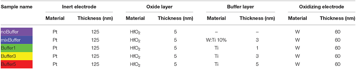
Table 1. Material stacks of all the tested devices.
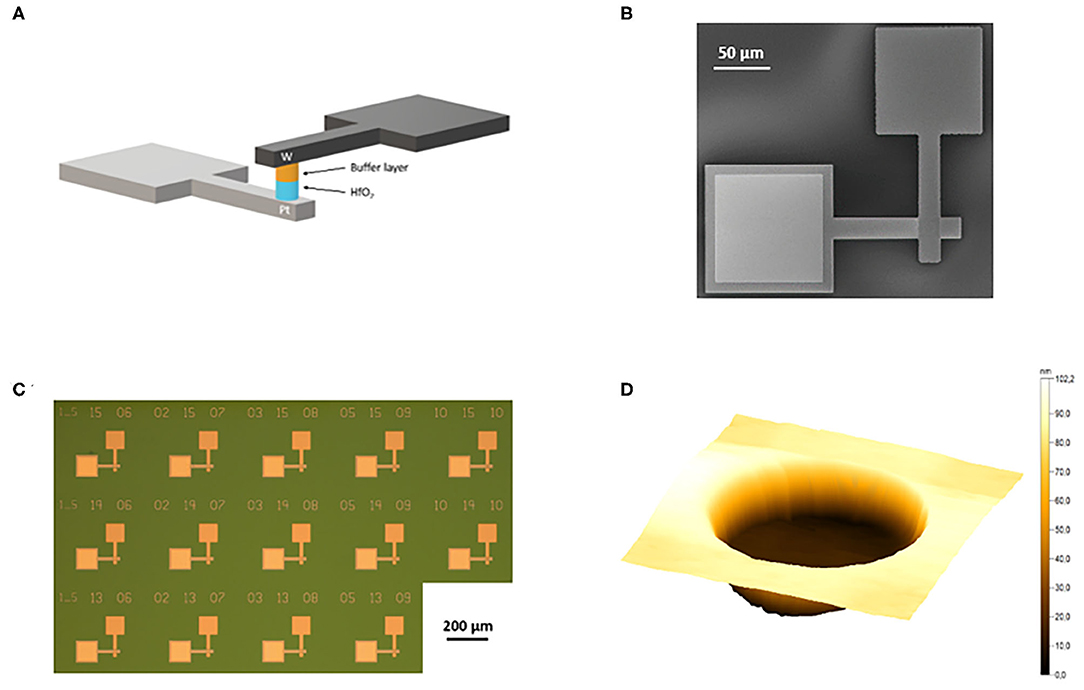
Figure 1. The cross-point geometry of the tested devices is shown through a 3D sketch (A) and a field emission scanning electron microscope (FESEM) image in top view (B). In the first case, the schematic, not to scale, focuses on a single device emphasizing the material stack, while in the second picture the actual geometry is shown. The periodic arrangement of the resistive random access memory (ReRAM) cells with all the different vertical interconnect access (VIA) dimensions is then highlighted by a micrograph (C). In (D), a single VIA with a diameter of 10 μm is shown by a topography image obtained with contact mode atomic force microscopy (AFM).
In order to carry out a complete performance analysis suited to compare the material stacks and investigate the effect of the Ti-based buffer layers, 25 devices for each sample were first subjected to a systematic DC characterization made of forming and cycling steps. Pristine devices underwent positive voltage sweeps from 0 to 7 V with a compliance current of 1 mA; then, bipolar voltage ramps ranging from −1.5 V to 3 V were applied to the same devices to test the cycling behavior. Bipolar resistive switching, with SET and RESET occurring in positive and negative polarity, respectively, was observed for all the devices regardless of the material stack. The latter, conversely, turned out to play a role in the definition of the device performance. First of all, an impact of the titanium-based buffer layers on the forming process was observed, with a decrease of the forming voltage (VFORMING) for thicker buffer layers (Figure 2A). Particularly, as presented by the box plot in Figure 2B, such a reduction turned out to be well-described by an exponential decay of the median values of VFORMING for the samples with pure Ti buffer layers. The same curve was then employed, the other way around, to define an effective thickness of the mixed buffer layer, which came out to be about 0.5 nm. Such an effective thickness, smaller than the real one of 3 nm, clarifies that the key player in the reduction of the forming voltage is not properly the thickness of the buffer layer but rather the presence, and the amount, of titanium between the hafnium dioxide film and the tungsten electrode.
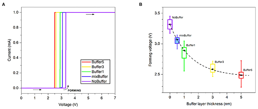
Figure 2. The median values of VFORMING for each material stack show a dependence of the forming process on the buffer layer. In (A), the corresponding I–V characteristics are shown, while in (B) their exponential decay as a function of the Ti-based buffer layer thickness is presented.
Consistent results were shown by the C-AFM characterization too. As reported in Figures 3A–C, three different stacks were investigated, namely NoBuffer, mixBuffer, and Buffer3, with the structure sketched in the insets of Figures 3A–C. As is clear from those pictures, the same MIM geometry as the one schematized in Figure 1A was reproduced thanks to the full-platinum AFM tip, which played the role of the inert electrode. By selecting such triplet of stacks, the key points of the previous analysis were further investigated. Indeed, with this set of devices, two main comparisons were possible, namely (i) the case with or without the buffer layer and (ii) the case of pure or mixed titanium with a fixed thickness. For each sample investigated by means of C-AFM, forming was induced first and current maps were produced afterwards. For both the measurements, the platinum tip was kept grounded and voltages were applied at the tungsten electrode. To achieve forming, voltage sweeps from 0 to 7 V were employed as for the analysis carried out through the parameter analyzer, with a current compliance set at 1 μA. Current maps were instead produced applying fixed voltages. Similarly to Figures 2A, 3A–C show a reduction of VFORMING depending on the presence of titanium between the oxidizing electrode and the oxide layer. Furthermore, in accordance with Figure 2B, such a reduction turned out to be related to the amount of titanium in the buffer layer rather than to the physical thickness of the Ti-based layer only. Indeed, both the buffer layers employed for the mixBuffer and Buffer3 samples are 3 nm thick, but their compositions differ from one another, with the mixBuffer sample exhibiting a tungsten film with 10% in weight of titanium instead of a pure Ti film. The current maps, produced after forming was induced, are then reported in Figures 3D–F. They show a nanometer-sized conductive spot for each sample, which strongly suggests a filamentary nature of the resistive switching in the tested devices. The topography images, acquired simultaneously with the creation of the current maps, are reported too (Figures 3G–I), and a superposition of the current maps on the topography images is presented in Figures 3J–L as the result of a point-by-point analysis of the electrical conduction. Particularly, in the case of Buffer3 samples, the presence of morphological changes is reported (Figure 3I), and Figure 3L highlights that such modifications turn out to perfectly match with the conductive spot found in the current map.
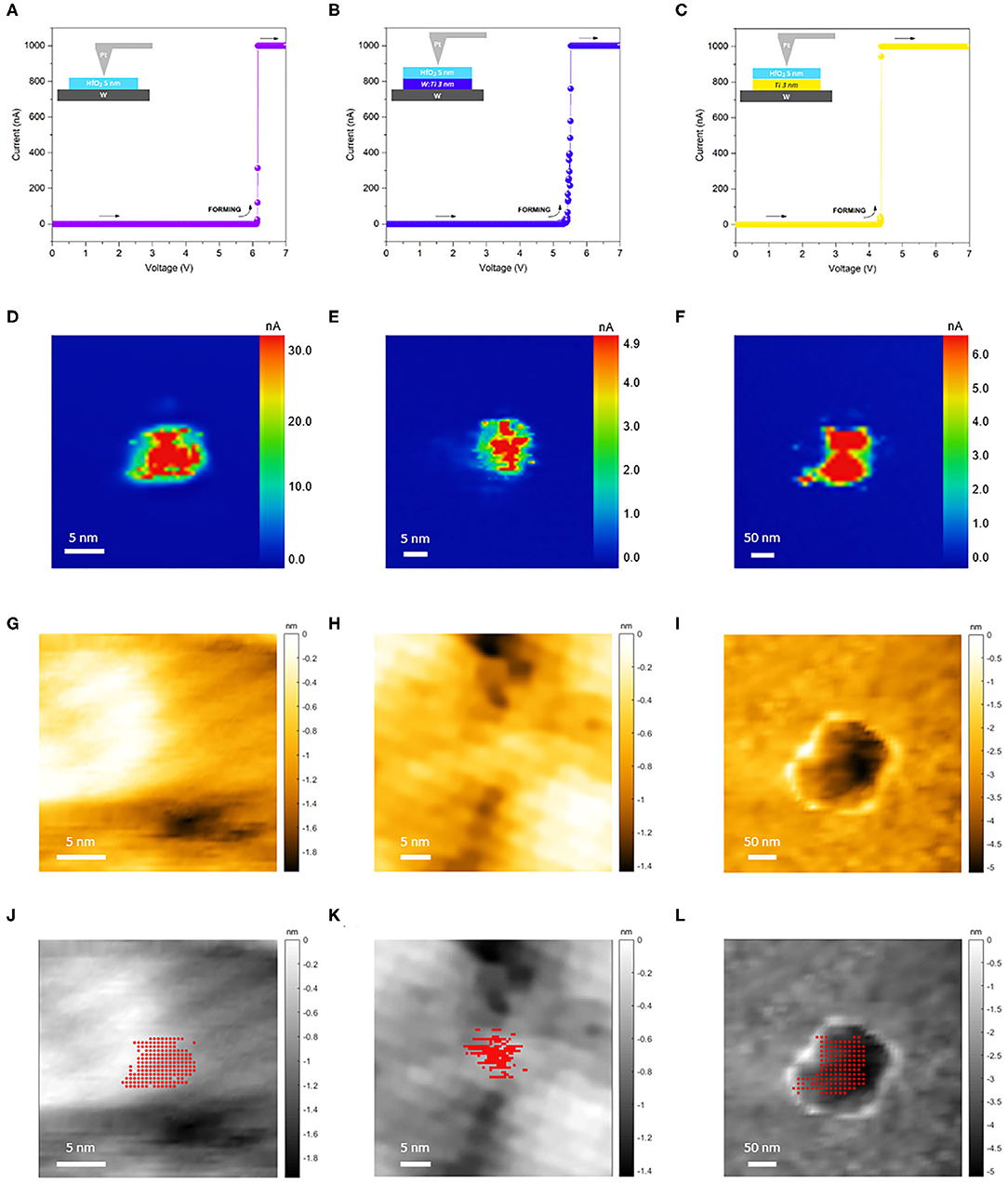
Figure 3. Investigation of the forming process was performed with conductive atomic force microscopy (C-AFM) directly probing the oxide layer by means of full-platinum tips. The resulting I–V characteristics are reported in (A–C), where VFORMING is reported to decrease with increasing amount of titanium in the buffer layer. In (D–F), the current maps acquired after the forming process are reported, with conductive spots clearly shown for all the tested material stacks. The topography images obtained at the same time with the current maps are then reported in (G–I), showing the presence of morphological changes in the case of the Buffer3 samples (I). In (J–L), the superposition of topographical and electrical images is presented.
Even though the C-AFM analysis clearly reported the presence, in all the tested material stacks, of conductive spots at the HfO2/Pt interface, suggesting resistive switching of filamentary type, a statistical DC characterization was performed to exclude a dependence of the RS on the device area as a consequence of interfacial effects at the W/HfO2 or buffer layer/HfO2 interface. By means of the parameter analyzer, bipolar voltage sweeps in the range −1.5 to 3 V were applied on 25 devices for the NoBuffer, mixBuffer, and Buffer5 samples. As summarized by the box plots in Figure 4, such characterization revealed that RS parameters like the resistance levels, VSET, and VRESET are independent of the device area since no correlation was found between these quantities and the diameter of the VIAs (1.5, 2, 3, 5, and 10 μm). Therefore, we can conclude that the observed resistive switching can be truly ascribed to a filamentary mechanism.
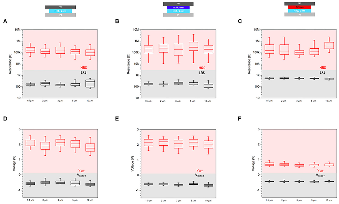
Figure 4. The resistance levels (A–C) and the switching voltages (D–F) for all the vertical interconnect access (VIA) diameters were compared in a triplet of material stacks: NoBuffer (A,D), mixBuffer (B,E), and Buffer5 (C,F).
Through the same DC characterization, that is to say applying consecutive cycles of bipolar voltage sweeps 0 V → −1.5 V → 3 V → 0 V, the switching behavior of the devices was investigated. As is reported in Figure 5, where I–V characteristics representative of a typical cycle for each material stack are shown, two different behaviors can be highlighted in the DC operation regime for Ti-based buffer layers thinner or thicker than 3 nm, respectively. More in detail, starting from Figure 5A, which reports the cycling behavior of the devices with no buffer layer, clear current fluctuations can be appreciated in the HRS for positive voltages. Interpreted from a different, but complementary, perspective, Figure 5A shows that the devices without a buffer layer exhibit some instability during the SET process, with sharp transitions from HRS to LRS occurring at relatively high voltages only after quick, repeated current variations. A similar behavior can be observed in the case of the mixBuffer (Figure 5B) and Buffer1 (Figure 5C) samples too, while a clear change occurs in the Buffer3 (Figure 5D) and Buffer5 (Figure 5E) samples. The latter two, indeed, still exhibit abrupt switching from HRS to LRS, but the sharp transition takes place at lower voltages and the I–V characteristics in HRS in positive polarity are much more stable, with no fluctuations. Moreover, as is graphically summarized in Figure 6A, which reports the statistical variations of VSET and VRESET obtained from the DC characterization, such improved stability in the device operation is coupled to a significantly reduced device-to-device variability.
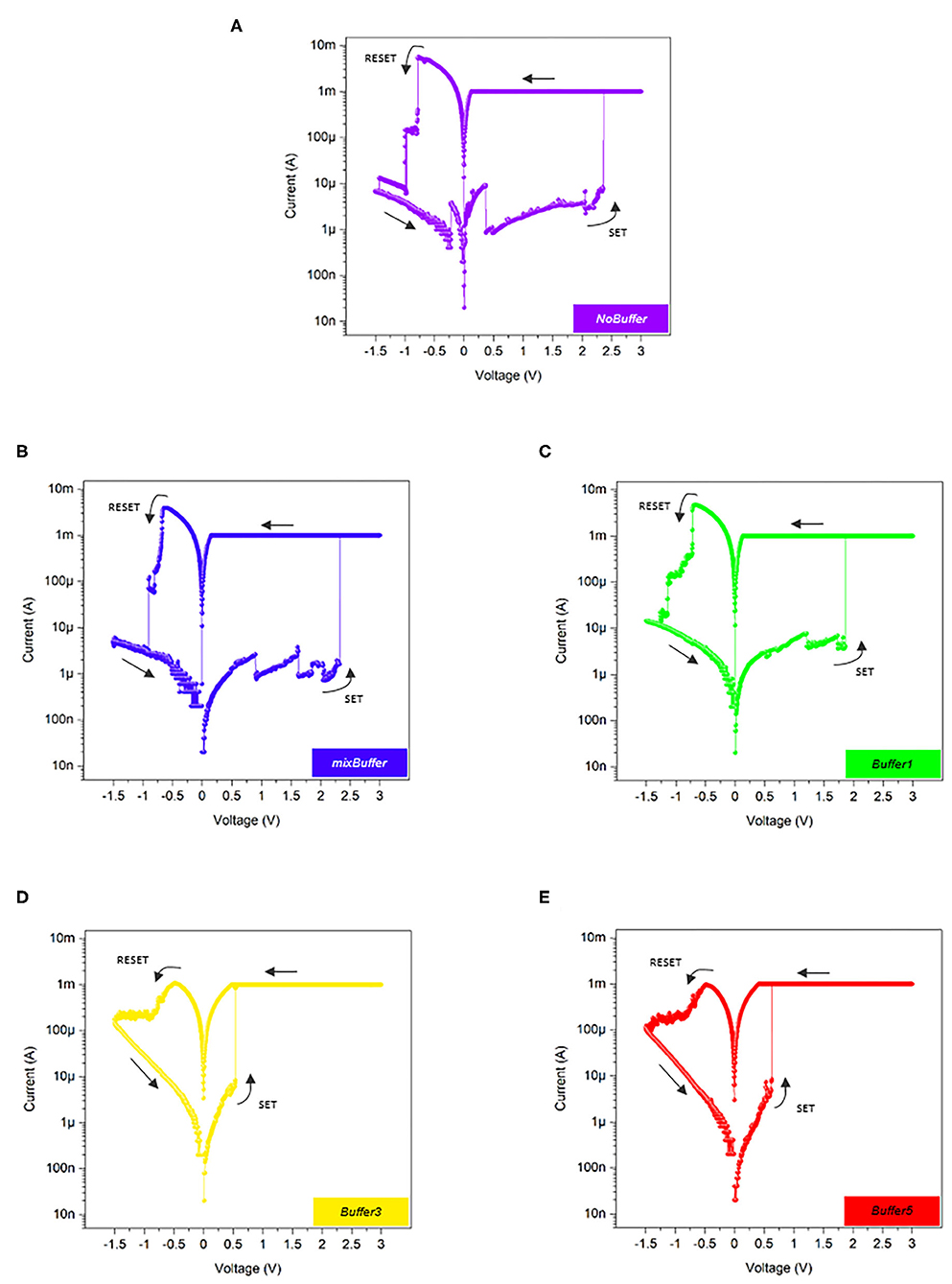
Figure 5. Applying bipolar voltage sweeps, the switching behavior of the tested device was investigated through the resulting I–V characteristics. The reported graphs are representative curves for each material stack. In the NoBuffer samples (A), current fluctuations occur before the SET process and RESET takes place abruptly. A similar behavior is shown by the mixBuffer (B) and Buffer1 (C) samples also. In the Buffer3 (D) and Buffer5 (E) samples, instead, the current fluctuations in the high-resistance state (HRS) in positive polarity are not observed; a lower VSET is found and gradual RESET occurs as it is flagged by a smooth current decrease for negative voltages close to VRESET.
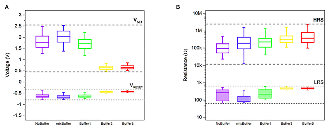
Figure 6. The statistical analysis of the DC characterization performed on 25 devices for each material stack is presented by means of box plots. In (A), the switching voltages are reported, while the resistance levels are shown in (B). In both cases, for the sake of clarity, dashed lines are employed to distinguish the different ranges of data.
The second major result arising from the insertion of a Ti-based buffer layer, which becomes apparent for Buffer3 and Buffer5 samples as for the HRS stability above-mentioned, involves the opposite polarity and the opposite transition. In Figures 5D,E, indeed, a fairly different behavior in the transition from LRS to HRS can be appreciated, with a gradual resistance variation instead of an abrupt switch. Interestingly, such change does not reflect into an increased device stability or reduced device-to-device variability. As reported in Figure 6A, indeed, differently from VSET, the RESET voltage does not significantly vary neither from a device to another nor from a sample to another. Similar observations can be made for the resistance values also, whose statistical analysis is reported in Figure 6B. In this case, the effect of Ti-based buffer layers as a stabilizer can be appreciated looking at the variability of the LRS in the different samples. As is clear from the box plot, the resistance value of the highly conductive state is significantly more stable in Buffer3 and Buffer5 samples, while a relevant device-to-device variability affects the devices based on the other material stacks.
The statistical parameters resulting from the DC characterization performed on a total of 125 devices are summarized in Table 2.
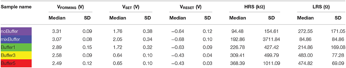
Table 2. Median values and standard deviations from the statistical DC characterization.
Based on reaction (1), both the current fluctuations before SET occurs and the gradual RESET can be interpreted referring to oxygen exchanges, which, in turn, involve the oxidizing activity of the layers in contact with the hafnium dioxide. Since, as already mentioned, one of these layers is always made of platinum, which is inert, the two phenomena must be related to the buffer layer, or to the tungsten electrode when the former is not present. In this view, the interpretation of the observed behavior in the DC regime can be traced back to the different oxidizing characteristics of titanium and tungsten. Current fluctuations may be related to the multiple, metastable oxides tungsten can form before reaching the stable WO3 (Lassner and Schubert, 1999; Shahrabi et al., 2019) since the emergence of such fluctuations can be appreciated in the NoBuffer, mixBuffer, and Buffer1 samples only. In the Buffer3 and Buffer5 samples, indeed, the thickness of the buffer layers is such that a large enough amount of titanium is present to effectively hinder the formation of metastable tungsten oxides (Shahrabi et al., 2019). On the other hand, concerning the transition from an abrupt to a gradual RESET, similar arguments hold, and the smoother resistance change can be again ascribed to the oxidizing behavior of the buffer layer. The gradual transition, indeed, takes place in the Buffer3 and Buffer5 samples only, that is to say, once more, only in those devices with a large enough amount of titanium between the tungsten electrode and the hafnium dioxide.
A further confirmation of the stabilizing effect given by the titanium buffer layer was then found with pulse tests aimed at investigating the endurance of the devices, namely their cycling reliability. For each material stack, an initial optimization procedure was first performed on the pulse parameters in order to find the best combinations of pulse width and pulse amplitude. As is shown in Figure 7, pulses were optimized for both SET and RESET since, as shown by the DC characterization, the bipolar RS of the tested devices is not symmetrical. Specifically, |VSET| turned out to be higher than |VRESET|, while identical pulse widths were used in both polarities. Finally, a delay of 200 ms was always employed between a pulse and the following one. Figure 7 clearly shows that such an optimization revealed a key impact of titanium on the dynamical operation regime of the tested devices. Indeed, besides the reduction of pulse amplitude needed for successful RS, which was already pointed out with the DC characterization, pure Ti buffer layers turned out to lead to a pulse width reduction down to three orders of magnitude with respect to the devices without a buffer layer.
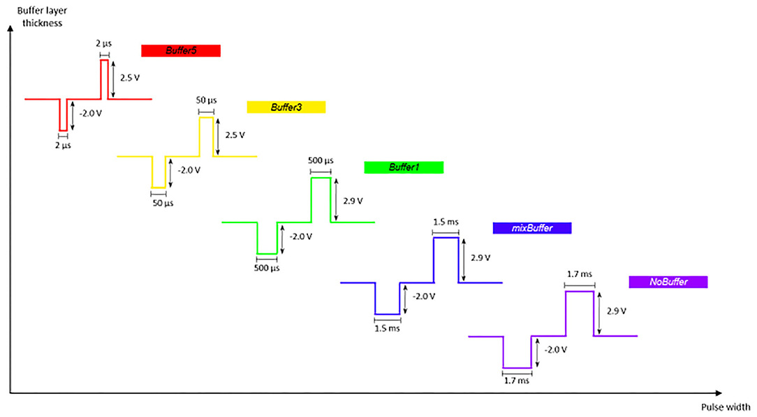
Figure 7. The insertion of buffer layers with increasing amount of titanium translates into a faster response of the devices, as shown by the pulse width reduction achieved with thicker Ti-based buffer layers.
Once the pulse parameter optimization was completed, a common test procedure was defined and adopted for all the material stacks, so that a clear performance comparison among the different samples was possible. Specifically, all the devices subjected to the endurance test were subjected to 2,000 SET–RESET pulse pairs aimed at continuously switching between HRS and LRS. The results of this characterization, reported in Figure 8, show how, besides improving the device stability, pure Ti buffer layers also have a beneficial effect on the endurance itself. Figures 8A,B, indeed, reveal that the NoBuffer and mixBuffer samples suffered for HRS failures preventing them from reaching the common test length of 2,000 cycles. Particularly, the devices from both material stacks were not able to overcome 1,500 cycles. Conversely, the Buffer1, Buffer3, and Buffer5 samples were all able to reach the fixed benchmark of 2,000 cycles, thus demonstrating an improvement of about 30%. Moreover, as already mentioned, the stability of the devices significantly improved, as is highlighted in Figures 8C–E by the much less scattered data as the amount of titanium in the buffer layers increases. A quantitative evaluation of the data dispersion can be made through the relative uncertainty (Table 3), which, in the case of HRS, turns out to be smaller than 100% for the Buffer3 and Buffer5 samples only. In more detail, such samples provide relative uncertainties of 87 and 41%, respectively, while 119% is found for the NoBuffer samples, 156% in the case of the mixBuffer ones, and 180% for the devices coming from the Buffer1 samples. The relative uncertainties are instead much smaller for the LRS during the endurance tests, and they do not show any trend related to the material stack.
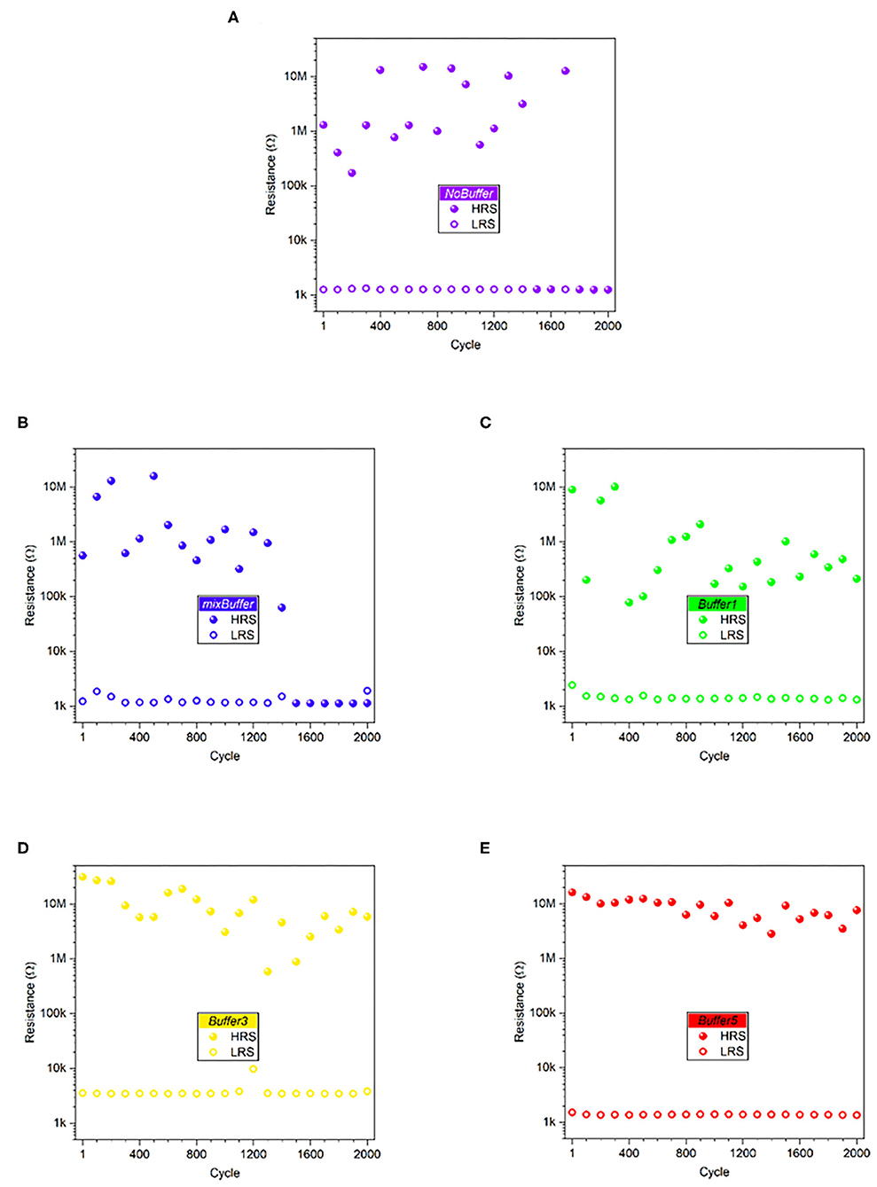
Figure 8. Endurance tests were performed with a fixed sequence of 2,000 SET–RESET pulse pairs. The NoBuffer (A) and mixBuffer (B) samples showed high-resistance state (HRS) failure after about 1,500 cycles, while the devices from the other material stacks (C–E) successfully completed the fixed-length test. Additionally, a stabilization of the HRS was observed for the Buffer1 (C), Buffer3 (D), and Buffer5 (E) samples.
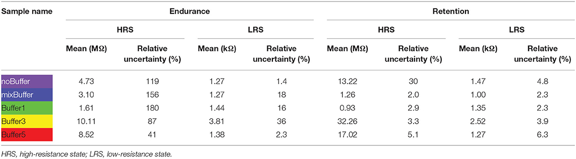
Table 3. Summary of resistance values during endurance and retention measurements.
To complete the set of electrical characterizations, retention tests were performed on new samples to compare the capability of the different material stacks of preserving each resistance state. A summary of the mean values, together with their relative uncertainties, for both HRS and LRS during pulse operations is presented in Table 3. As for the endurance, a common benchmark was set for the retention tests too, and 2 × 10⁴ s was adopted as the fixed length for the measurements in order to define a standard procedure for all the samples. The results are shown in Figure 9, where a good stability is reported for all the material stacks. In this case, no significant difference can be appreciated depending on the buffer layer, with all the devices able to reach the fixed value of 2 × 10⁴ s and small relative uncertainties on the resistance values, in both HRS and LRS. As a consequence, the retention tests, which rely on the stability of the conductive filament rather than on its formation and rupture, seem to suggest that the Ti-based buffer layers actively play a role only when oxygen exchanges, as in reaction (1), occur, while they remain silent otherwise. The performance tunability and improvement titanium allows to achieve can hence be directly related to the stabilization of the interactions between the oxidizing electrode and the oxide layer. Compared to tungsten, titanium indeed requires a much lower energy to create oxygen vacancies in HfO2, and this significantly hinders the slower tungsten oxidation (Kim et al., 2016). As a consequence, titanium efficiently mitigates the fluctuations induced by the formation of metastable tungsten oxides (Lassner and Schubert, 1999) and allows faster responses from the devices.
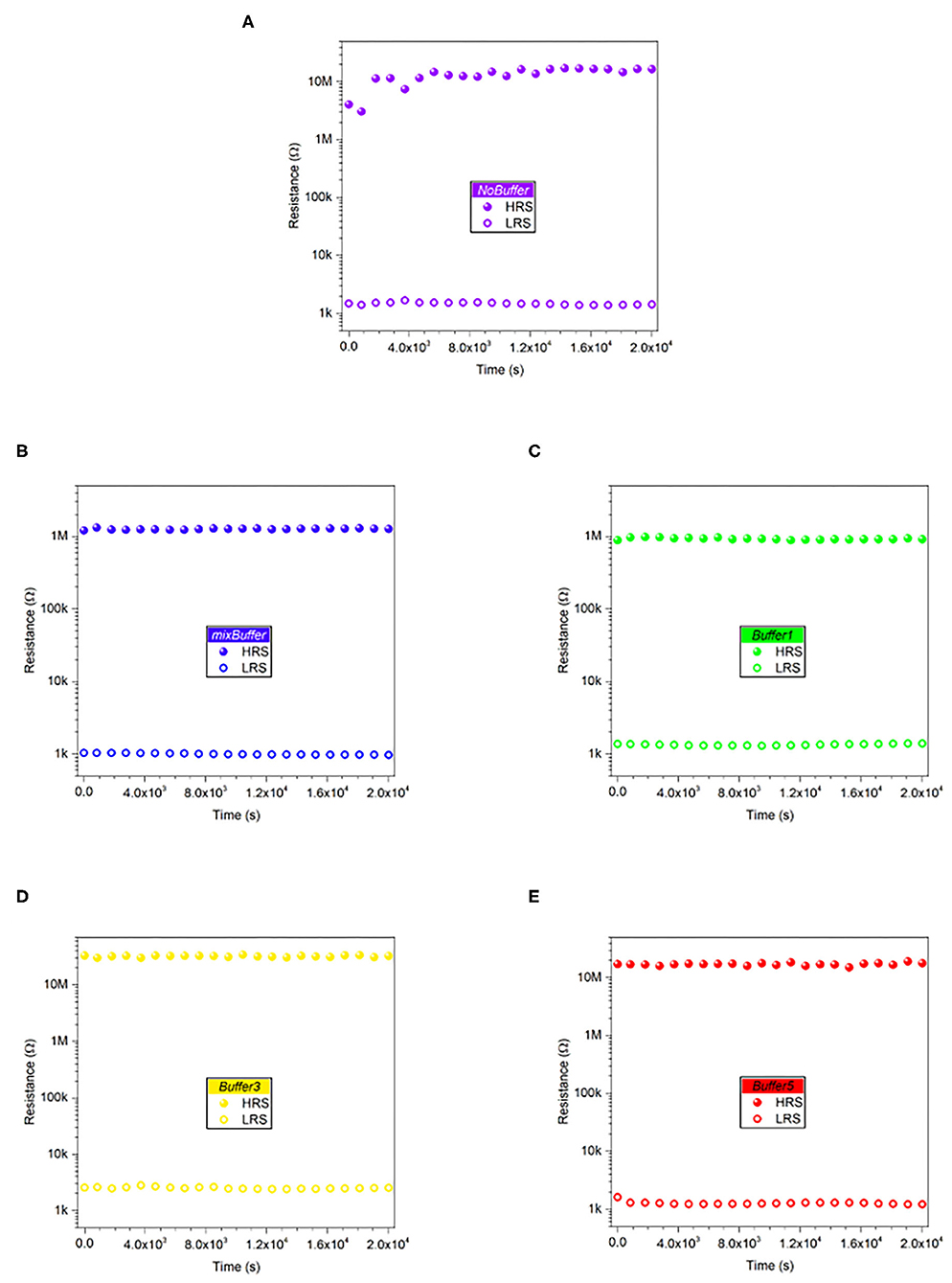
Figure 9. (A–E) Retention measurements, performed for a fixed time of 2 × 10⁴ s, highlighted that a good resistance state stability is provided by all the material stacks, with no significant contribution given by titanium.
Discussion
With this work, we have shown how titanium can be employed, as a buffer layer, to stabilize and tune the RS performances of ReRAM cells based on CMOS-compatible materials like HfO2 and tungsten. With an extensive, systematic approach, 125 devices with different material stacks have been tested. Investigating different thicknesses and compositions of the Ti-based films, a dependence of the device performances on the buffer layer properties was found, and the amount of titanium in the buffer layer turned out to play a key role. The presented results can be ascribed to the different oxidizing characteristics of titanium and tungsten. The latter, indeed, suffers from a relatively slower oxidation process, producing a variety of metastable oxides, responsible for the RS instability which clearly appears in both DC switching and pulse operations. Employing buffer layers with a high enough amount of titanium, relevant changes in the device performances have been reported. More in detail, the response speed has been shown to significantly increase according to the pulse width reduction of three orders of magnitude; an improvement of about 30% has been achieved in terms of endurance performance, and an increased stability of the resistance states, especially the HRS, has been obtained in the dynamic operation regime. In light of these results, the Ti buffer/W stack turns out to be a suitable choice for CMOS-compatible ReRAM cells that have to solve reliability issues coming from tungsten electrodes. Furthermore, the possibility of tuning the device performances according to the Ti-based buffer layer properties may open the way to the definition of new design rules for ReRAM integration with standard CMOS technology.
Data Availability Statement
The raw data supporting the conclusions of this article will be made available by the authors, without undue reservation.
Author Contributions
VF and ES contributed to the design and fabrication of the devices. VF performed device characterization. VF and CR wrote and revised the manuscript. CR and YL helped with supervision. All authors contributed to the article and approved the submitted version.
Funding
This research was partially supported by Compagnia di San Paolo through the project for internationalization of research of Politecnico di Torino.
Conflict of Interest
The authors declare that the research was conducted in the absence of any commercial or financial relationships that could be construed as a potential conflict of interest.
Acknowledgments
The help and the technical support given by the staff of the Center of Micro-nano Technology (CMi) of EPFL are gratefully acknowledged. A hearthfelt thank goes to P. Charpilloz for his supervision during AFM measurements.
References
Ambrosi, E., Bricalli, A., Laudato, M., and Ielmini, D. (2019). Impact of oxide and electrode materials on the switching characteristics of oxide ReRAM devices. Faraday Discuss. 213, 87–98. doi: 10.1039/C8FD00106E
Baek, I. G., Lee, M. S., Sco, S., Lee, M. J., Seo, D. H., Suh, D.-S., et al. (2005). “Highly scalable non-volatile resistive memory using simple binary oxide driven by asymmetric unipolar voltage pulses,” in IEDM Technical Digest. IEEE International Electron Devices Meeting, 2004. (San Francisco, CA), 587–590.
Cai, F., Correll, J. M., Lee, S. H., Lim, Y., Bothra, V., Zhang, Z., et al. (2019). A fully integrated reprogrammable memristor–CMOS system for efficient multiply–accumulate operations. Nat. Electron 2, 290–299. doi: 10.1038/s41928-019-0270-x
Celano, U., Fantini, A., Degraeve, R., Jurczak, M., Goux, L., and vandervorst, W. (2016). Scalability of valence change memory: from devices to tip-induced filaments. AIP Adv. 6:085009. doi: 10.1063/1.4961150
Celano, U., Gastaldi, C., Govoreanu, B., Richard, O., Bender, H., Goux, L., et al. (2017). Evidences of areal switching in vacancy-modulated conductive oxide (VMCO) memory. Microelectron. Eng. 178, 122–124. doi: 10.1016/j.mee.2017.04.046
Celano, U., Goux, L., Belmonte, A., Opsomer, K., Franquet, A., Schulze, A., et al. (2014). Three-dimensional observation of the conductive filament in nanoscaled resistive memory devices. Nano Lett. 14, 2401–2406. doi: 10.1021/nl500049g
Chen, Y., Li, L., Yin, X., Yerramilli, A., Shen, Y., Song, Y., et al. (2017). Resistive switching characteristics of flexible TiO2 thin film fabricated by deep ultraviolet photochemical solution method. IEEE Electron Device Lett. 38, 1528–1531. doi: 10.1109/LED.2017.2756444
Chen, Y. S., Lee, H. Y., Chen, P. S., Gu, P. Y., Chen, C. W., Lin, W. P., et al. (2009). “Highly scalable hafnium oxide memory with improvements of resistive distribution and read disturb immunity,” in Tech Dig Int Electron Devices Meet IEDM (Baltimore, MD), 105–108. doi: 10.1109/IEDM.2009.5424411
Chen, Y. Y., Goux, L., Clima, S., Govoreanu, B., Degraeve, R., Kar, G. S., et al. (2013). Endurance/retention trade-off on HfO2/Metal Cap 1T1R Bipolar RRAM. IEEE Trans. Electron Device 60, 1114–1121. doi: 10.1109/TED.2013.2241064
Conti, D., Laurenti, M., Porro, S., Giovinazzo, C., Bianco, S., Fra, V., et al. (2019). Resistive switching in sub-micrometric ZnO polycrystalline films. Nanotechnology 30:065707. doi: 10.1088/1361-6528/aaf261
Gibbons, J. F., and Beadle, W. E. (1964). Switching properties of thin NiO films. Solid State Electron 7, 785–790. doi: 10.1016/0038-1101(64)90131-5
Gilmer, D. C., Bersuker, G., Park, H. Y., Park, C., Butcher, B., Wang, W., et al. (2011). “Effects of RRAM stack configuration on forming voltage and current overshoot,” in 2011 3rd IEEE Int Mem Work IMW (Monterey, CA), 1–4. doi: 10.1109/IMW.2011.5873225
Govoreanu, B., Redolfi, A., Zhang, L., Adelmann, C., Popovici, M., Clima, S., et al. (2017). “Vacancy-modulated conductive oxide resistive RAM (VMCO-RRAM): an area-scalable switching current, self-compliant, highly nonlinear and wide on/off-window resistive switching cell,” in 2013 IEEE International Electron Devices Meeting (Washington, DC: IEEE), 10.2.1–10.2.4.
Guo, Y., and Robertson, J. (2014). Materials selection for oxide-based resistive random access memories. Appl. Phys. Lett. 105:223516. doi: 10.1063/1.4903470
Ielmini, D., and Waser, R. (2016). Resistive Switching. Weinheim, Germany: Wiley-VCH Verlag GmbH & Co. KGaA. doi: 10.1002/9783527680870
Joshua Yang, J., Miao, F., Pickett, M. D., Ohlberg, D. A. A., Stewart, D. R., Lau, C. N., et al. (2009). The mechanism of electroforming of metal oxide memristive switches. Nanotechnology 20:215201. doi: 10.1088/0957-4484/20/21/215201
Kim, W., Menzel, S., Wouters, D. J., Guo, Y., Robertson, J., Roesgen, B., et al. (2016). Impact of oxygen exchange reaction at the ohmic interface in Ta 2 O 5 -based ReRAM devices. Nanoscale 8, 17774–17781. doi: 10.1039/C6NR03810G
Kindsmüller, A., Meledin, A., Mayer, J., Waser, R., and Wouters, D. J. (2019). On the role of the metal oxide/reactive electrode interface during the forming procedure of valence change ReRAM devices. Nanoscale 11, 18201–18208. doi: 10.1039/C9NR06624A
Lamb, D. R., and Rundle, P. C. (1967). A non-filamentary switching action in thermally grown silicon dioxide films. Br. J. Appl. Phys. 18, 29–32. doi: 10.1088/0508-3443/18/1/306
Lassner, E., and Schubert, W.-D. (1999). Tungsten. Boston, MA: Springer US. doi: 10.1007/978-1-4615-4907-9
Lee, J. H., Wu, C., Sung, S., An, H., and Kim, T. W. (2019). Highly flexible and stable resistive switching devices based on WS2 nanosheets:poly(methylmethacrylate) nanocomposites. Sci. Rep. 9:19316. doi: 10.1038/s41598-019-55637-2
Lee, M.-J., Kang, B. S., Ahn, S.-E., Kim, K. H., Lee, C. B., Kim, C. J., et al. (2009). Electrical manipulation of nanofilaments in transition-metal oxides for resistance-based memory. Nano Lett. 9, 1476–1481. doi: 10.1021/nl803387q
Lin, Y. S., Zeng, F., Tang, S. G., Liu, H. Y., Chen, C., Gao, S., et al. (2013). Resistive switching mechanisms relating to oxygen vacancies migration in both interfaces in Ti/HfOx/Pt memory devices. J. Appl. Phys. 113:064510. doi: 10.1063/1.4791695
Marconi, G. (1899). Wireless telegraphy. J. Inst. Electr. Eng. 28, 273–290. doi: 10.1049/jiee-1.1899.0010
Meena, J. S., Sze, S. M., Chand, U., and Tseng, T. Y. (2014). Overview of emerging nonvolatile memory technologies. Nanoscale Res. Lett. 9:526. doi: 10.1186/1556-276X-9-526
Nafria, M., Rodriguez, R., Porti, M., Martin-Martinez, J., Crespo-Yepes, A., Claramunt, S., et al. (2017). (Invited) advanced measurement techniques for the characterization of ReRAM devices. ECS Trans. 79, 139–148. doi: 10.1149/07901.0139ecst
Rahaman, S. Z., Lin, Y.-D., Lee, H.-Y., Chen, Y.-S., Chen, P.-S., Chen, W.-S., et al. (2017). The role of Ti buffer layer thickness on the resistive switching properties of hafnium oxide-based resistive switching memories. Langmuir 33, 4654–4665. doi: 10.1021/acs.langmuir.7b00479
Shahrabi, E., Giovinazzo, C., Hadad, M., LaGrange, T., Ramos, M., Ricciardi, C., et al. (2019). Switching kinetics control of W-based ReRAM cells in transient operation by interface engineering. Adv Electron Mater. 5:1800835. doi: 10.1002/aelm.201800835
Singh, A. K., Blonkowski, S., and Kogelschatz, M. (2018). Resistive switching study in HfO2 based resistive memories by conductive atomic force microscopy in vacuum. J. Appl. Phys. 124, 014501. doi: 10.1063/1.5025143
Sun, Y. M., Song, C., Yin, J., Qiao, L. L., Wang, R., Wang, Z. Y., et al. (2019). Modulating metallic conductive filaments via bilayer oxides in resistive switching memory. Appl. Phys. Lett. 114:193502. doi: 10.1063/1.5098382
Tang, J., Yuan, F., Shen, X., Wang, Z., Rao, M., He, Y., et al. (2019). Bridging biological and artificial neural networks with emerging neuromorphic devices: fundamentals, progress, and challenges. Adv. Mater. 31:1902761. doi: 10.1002/adma.201902761
Tappertzhofen, S., Waser, R., and Valov, I. (2014). Impact of the counter-electrode material on redox processes in resistive switching memories. ChemElectroChem 1, 1287–1292. doi: 10.1002/celc.201402106
Tirano, S., Perniola, L., Buckley, J., Cluzel, J., Jousseaume, V., Muller, C., et al. (2011). Accurate analysis of parasitic current overshoot during forming operation in RRAMs. Microelectron. Eng. 88, 1129–1132. doi: 10.1016/j.mee.2011.03.062
Valov, I. (2014). Redox-based resistive switching memories (ReRAMs): Electrochemical systems at the atomic scale. ChemElectroChem 1, 26–36. doi: 10.1002/celc.201300165
Valov, I., Waser, R., Jameson, J. R., and Kozicki, M. N. (2011). Electrochemical metallization memories—fundamentals, applications, prospects. Nanotechnology 22:254003. doi: 10.1088/0957-4484/22/28/289502
Walczyk, D., Bertaud, T., Sowinska, M., Lukosius, M., Schubert, M. A., Fox, A., et al. (2012). “Resistive switching behavior in TiN/HfO2/Ti/TiN devices,” in 2012 International Semiconductor Conference Dresden-Grenoble (ISCDG) (Grenoble: IEEE), 143–146. doi: 10.1109/ISCDG.2012.6360035
Wang, Z., Wu, H., Burr, G. W., Hwang, C. S., Wang, K. L., Xia, Q., et al. (2020). Resistive switching materials for information processing. Nat. Rev. Mater. 5, 173–195. doi: 10.1038/s41578-019-0159-3
Waser, R., and Aono, M. (2007). Nanoionics-based resistive switching memories. Nat. Mater. 6, 833–840. doi: 10.1038/nmat2023
Wong, H. S. P., Lee, H. Y., Yu, S., Chen, Y. S., Wu, Y., Chen, P. S., et al. (2012). Metal-oxide RRAM. Proc. IEEE 100, 1951–1970. doi: 10.1109/JPROC.2012.2190369
Xia, Q., and Yang, J. J. (2019). Memristive crossbar arrays for brain-inspired computing. Nat. Mater. 18, 309–323. doi: 10.1038/s41563-019-0291-x
Yang, J. J., Zhang, M. X., Strachan, J. P., Miao, F., Pickett, M. D., Kelley, R. D., et al. (2010). High switching endurance in TaOx memristive devices. Appl. Phys. Lett. 97, 6–9. doi: 10.1063/1.3524521
Yen, T. J., Gismatulin, A., Volodin, V., Gritsenko, V., and Chin, A. (2019). All nonmetal resistive random access memory. Sci. Rep 9:6144. doi: 10.1038/s41598-019-42706-9
Keywords: resistive switching, ReRAM, tungsten, titanium, buffer layer
Citation: Fra V, Shahrabi E, Leblebici Y and Ricciardi C (2020) Investigation on the Stabilizing Effect of Titanium in HfO2-Based Resistive Switching Devices With Tungsten Electrode. Front. Nanotechnol. 2:592684. doi: 10.3389/fnano.2020.592684
Received: 07 August 2020; Accepted: 29 September 2020;
Published: 30 October 2020.
Edited by:
J. Joshua Yang, University of Southern California, Los Angeles, United StatesReviewed by:
Massood Atashbar, Western Michigan University, United StatesAbhay A. Sagade, SRM Institute of Science and Technology, India
Copyright © 2020 Fra, Shahrabi, Leblebici and Ricciardi. This is an open-access article distributed under the terms of the Creative Commons Attribution License (CC BY). The use, distribution or reproduction in other forums is permitted, provided the original author(s) and the copyright owner(s) are credited and that the original publication in this journal is cited, in accordance with accepted academic practice. No use, distribution or reproduction is permitted which does not comply with these terms.
*Correspondence: Carlo Ricciardi, Y2FybG8ucmljY2lhcmRpQHBvbGl0by5pdA==