 Ya-Chu Lee1
 Chingfu Tsou
 Weileun Fang
95% of researchers rate our articles as excellent or good
Learn more about the work of our research integrity team to safeguard the quality of each article we publish.
Find out more
ORIGINAL RESEARCH article
Front. Mech. Eng. , 17 May 2022
Sec. Micro- and Nanoelectromechanical Systems
Volume 8 - 2022 | https://doi.org/10.3389/fmech.2022.894060
This article is part of the Research Topic Design and Analysis of CMOS-MEMS Transducers View all 9 articles
Environmental sensing units such as gas sensors, humidity sensors, pressure sensors, PM 2.5 sensors, or temperature sensors are widely used in our daily lives. In this study, CMOS-MEMS technology is exploited to fabricate and monolithically integrate the photo-sensors, temperature sensor, and mechanical structures for an optical gas sensing chip. An LED is bonded (heterogeneous integration) on the CMOS-MEMS chip as an excitation light source, and fluorescence quenching technology is employed for the presented optical gas sensor. Finally, the light emitted from the LED is reflected and redirected onto the CMOS-MEMS chip by using an encapsulated optical reflector to increase the sensitivity and reduce the power consumption for the presented sensor. In applications, the sensing materials are, respectively, mixed with C30H24Cl2N6Ru·6H2O and C16H7Na3O10S3 for O2 and CO2 detection. Moreover, the Si-based (by micromachining) and polymer-based (by 3D printing) optical reflectors are used to encapsulate the sensing chip to demonstrate the presented concept. Measurements show that the LED driving currents for gas sensors with reflectors are significantly reduced. Measurements also indicate that the sensitivities of gas sensors for sensing chips without optical reflectors are, respectively, 0.023 μA/% (O2/N2) and 0.12 μA/% (CO2/N2); for sensing chips with hemispherical shell optical reflectors are, respectively, 0.12 μA/% (O2/N2) and 0.19 μA/% (CO2/N2); and for sensing chips with flat plate optical reflectors are, respectively, 0.24 μA/% (O2/N2) and 0.32 μA/% (CO2/N2). The sensitivity of the temperature sensor is 0.07%/°C.
Gas sensors have been widely utilized in various applications, such as automobile, industrial, medical, agricultural, and environmental applications (Gas Sensor Applications, 2021) (SST Sensing Ltd., 2021). For instance, gas sensors could be installed in living rooms, bathrooms, kitchens, etc. for environmental monitoring to realize smart homes for improvement in the quality and safety of our daily lives. Gas sensors could also be employed to monitor the air quality of public and private domains. Thus, gas sensors are considered as a promising component for internet of things (IoT) applications and have the potential to be integrated onto smart phones and devices. Many gas detection technologies have been developed, such as electrochemical (Wan et al., 2018) (Paul et al., 2020), calorimetric (Bartlett and Guerin, 2003), optical-based (Wang et al., 2021) (Chang et al., 2018) (Jorge et al., 2004) (McDonagh et al., 2002), and acoustic-based (Arsat et al., 2009) devices. Among the aforementioned sensing mechanisms, optical detection technologies (including infrared and chemi-luminescence approaches) have the advantages of higher sensitivity and faster response. However, bulky size and relatively high cost are two concerns for optical sensing technologies.
The standard complementary metal-oxide semiconductor (CMOS) processes are mature fabrication technologies offered by many foundries. To date, the CMOS processes have been extended to implement micro-electro-mechanical-systems (MEMS) chips by adding several additional fabrication steps (post-CMOS processes, such as the wet and dry etching on thin films and the Si substrate) (Fedder, 2005) (Fang et al., 2021). In this regard, the monolithic integration of the integrated circuit (IC) and sensing components on a single chip can be achieved (Tzeng et al., 2016) (Lee et al., 2021a). This CMOS-MEMS technology exhibits various advantages, for instance, multiple metal and dielectric layers are available to offer the design flexibility for MEMS structures and electrical routing; and many sensing mechanisms can be realized by the inherent materials of the CMOS process such as the metal/dielectric films, and boron/phosphorus-doped poly-silicon. Various miniaturized environment sensors and sensing hubs have been demonstrated using the CMOS-MEMS approach (Lin et al., 2020), including the gas sensors in Chien et al. (2022). Thus, CMOS-MEMS is a promising technology to achieve the size and cost reduction requirements for gas sensors.
This study extends the concept in Lee et al. (2017); Lee et al. (2019) to adopt the CMOS-MEMS technology to design and implement optical gas sensors. Various key components such as photo-sensors, mechanical structures, and temperature sensors will be integrated on the sensing chip through CMOS-MEMS processes. Based on the TSMC (Taiwan Semiconductor Manufacturing Corp.) 0.35 µm 2P4M (two poly-Si layer and four metal layers) standard processes, the CMOS chip is designed and implemented. The in-house post-CMOS micromachining processes are also developed to realize the gas sensing chip. In addition, this study will also exploit the method of heterogeneous integration to bond an LED (light emitting diode) chip as the light emitting source on the CMOS-MEMS gas sensing chip, through which the size reduction of the optical gas sensor can be achieved. Sensing materials are prepared to realize the fluorescence quenching-based optical gas sensors. To further enhance the performance of the CMOS-MEMS chemi-luminescence gas sensor, this study also exploits the solution in Lee et al. (2021b) to encapsulate the CMOS-MEMS sensing chip by using light reflectors. Thus, the light emitted from the LED chip is reflected and redirected onto the CMOS-MEMS chip by an encapsulated optical reflector to increase the sensitivity and reduce the power consumption for the presented sensor.
The presented sensing chip is designed based on the design rules of standard CMOS processes offered by the foundry. The in-house post-CMOS micromachining and assembly processes are also employed to implement the presented gas sensor shown in Figure 1. As illustrated in Figure 1A, the presented gas sensor consists of the gas sensing chip attached to the PCB (printed circuit board), the blue LED bonded on the central stage of sensing chip, and the light reflector. This study presents and discusses the hemispherical shell and flat plate light reflector designs. The sensing chip consists of a cavity array filled with gas sensing films, the photo-sensors (photodiode element) embedded at the bottom of each cavity, and the RTD (resistance temperature detector). Furthermore, the trenches between the cavity and LED are designed to prevent the overflow of gas sensing materials during dispensing. The cross-section AA’ in Figure 1B indicates that the cavity array could be filled with different sensing films to detect multiple gases. As depicted by the cross-section BB’ in Figure 1C, the photo-sensor will generate the photo-current I0 when the LED light is incident on the reference cavity (cavity with no sensing film). An additional photo-current If will be introduced as the cavity is filled with the sensing material used in this study (sensing cavity). The photo-current If is contributed from the fluorescence of the sensing film. When the gas to be detected is absorbed by the sensing film, fluorescence quenching occurs, causing the photo-current If to drop to If’. Therefore, the gas to be detected is determined by the photo-current If’ which can be measured by subtracting the sensing photo-current (I0+If’) and the reference photo-current (I0).
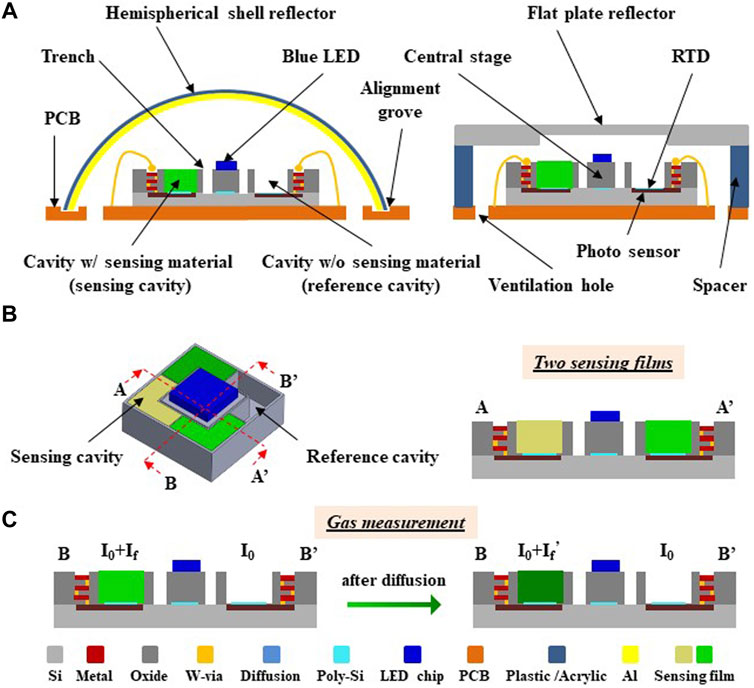
FIGURE 1. (A) Schematic of the presented gas sensor design consisted of the CMOS-MEMS gas sensing chip, the sensing material, the LED chip, and the light reflectors, (B) schematic of the presented CMOS-MEMS gas sensing chip with sensing materials in an isometric view and cross-sectional view.
This study exploits the principle of fluorescence quenching (Jorge et al., 2004) for gas sensing. In this approach, molecules of sensing material will transit from the ground state to the excited state when absorbing a given light. As molecules of sensing material transit back to the ground state, radiation (i.e., fluorescence) will be emitted. The fluorescence intensity will be decreased if the sensing material absorbed the gas to be detected. Thus, the gas concentration can be determined by the variation of fluorescence intensity. Accordingly, the gas to be detected acts as the quencher to inhibit the intensity of fluorescence and operates according to the Stern-Volmer relation (Lakowicz, 2006) (Chu and Lo, 2008)
where F0 and F are the fluorescence intensities, respectively, for the absence and the presence of gas, (Q) is the gas (quencher) concentration, and K is the Stern-Volmer coefficient. Thus, as the fluorescence intensities are determined by the measured photo-current, the gas concentration can be extracted from Eq. 1. Note that photo-sensors in Figure 1 are realized using the Si substrate with doped N+/P+ inherent in the CMOS process. According to Olson et al. (2003), the upper cut-off wavelength λg of the photo-sensor can be expressed as
where Eg is 1.12 eV in this study, h is the Planck’s constant, and c is the speed of light (2.998 × 10⁸ m/s). Thus, the upper cut-off wavelength λg is 1.11 µm. Moreover, sensing materials are fluorophore compounds which could emit fluorescence upon light excitation. In applications, O2 and CO2 detection is demonstrated by the presented gas sensors, and C30H24Cl2N6Ru·6H2O and C16H7Na3O10S3 will be used as the sensing materials. Since the sensing materials have the light excitation wavelengths (λexc) of 470 nm (for O2) and 460 nm (for CO2) (Jorge et al., 2004) (Nivens et al., 2002), the blue LED with a wavelength of 445–455 nm is selected. In addition, the fluorescence emitted from sensing materials has the wavelengths (λemi) of 610 nm (for O2) and 520 nm (for CO2). These wavelengths fulfill the requirement of being smaller than λg.
The light source of the blue LED is mainly top-emitting (Chu et al., 2015) (Liou and Tsou, 2018). To enhance the sensing signal, an optical reflector (two different designs) is employed to cover the sensing chip through the packaging process. Thus, the light emitted from the top-side of the LED could be reflected back and redirected to the sensing chip and photo-sensors. This study employs the commercial software TracePro to predict the light path and intensity. To compare the light intensity and distribution of the designs with and without covers, as depicted in Figure 2, the same incident light emitted from the LED is established in simulation models. The optical reflector has a diameter of 20 mm (to enable manually assembly). Simulations in Figures 2A–C show the light intensity distribution on the sensing chip for these three designs. With the assistance of the optical reflector, the designs in Figures 2B,C have higher light intensity in the regions of photo-sensors. The results in Figure 2D further indicate that the maximum light intensities of these three designs within the photo sensing area are, respectively, 8.4 × 10⁷ lux (no light reflector), 1.07 × 10⁸ lux (hemispherical shell), and 1.82 × 10⁸ lux (flat plate). Thus, the proposed designs with the optical reflector could offer the advantage of improved responsivity.
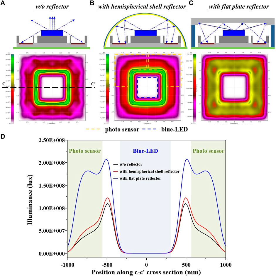
FIGURE 2. Schematic of the light path emitted from the LED to the gas sensing chip and simulation results of the illuminance map for three different gas sensor designs, (A) for the gas sensing chip without reflector, (B,C) respectively, for gas sensing chips with the hemispherical shell and the flat plate reflectors, and (D) simulation results of the light intensity changes.
Figure 3 shows the micromachining processes to implement the proposed gas sensor. Figure 3A depicts the chip fabricated using the standard 0.35 μm 2P4M CMOS processes by the TSMC. The stacking and patterning of multiple Al and SiO2 layers, and tungsten vias are observed. The sacrificial layers consisted of Al metal films; and tungsten vias were then removed by the metal wet etching solution (H2SO4 and H2O2) (Tsai et al., 2009). After that, the structures to act as the cavity array and the stage for LED mounting were realized, as illustrated in Figure 3B. The photo-sensors and RTDs are also exhibited in this chip. As depicted in Figure 3C, the dielectric film was removed by reactive ion etching (RIE) to expose bonding pads for electrical routing of photo-sensors and RTDs. The blue LED chip was then assembled on the stage, as indicated in Figure 3D. In this study, the LED was manually placed on the CMOS-MEMS chip and then bonded by glue. Note that the LED could be bonded on the CMOS-MEMS chip by using the mature pick-and-place technology provided by the commercial packaging houses. The wire bonding between the sensing chip and the PCB board was performed in the process of Figure 3E, and then the sensing chip was deposited with sensing material and baked at the 40°C for 12 h, as show in Figure 3F. Finally, the fabrication and bonding processes for two different optical deflector designs are illustrated in Figure 3G. As displayed in Figure 3Gi, the hemispherical shell optical reflector was bonded to the circular groove on the PCB to cover the fabricated sensing chip. The hemispherical shell plastic optical reflector was fabricated using the 3D printer and then evaporated with the metal film on its inner surface to enhance the light reflection. As shown in Figure 3Gii, the flat plate optical reflector was manually bonded to the PCB through a spacer to cover the fabricated sensing chip. The flat plate optical reflector uses the photolithography process to define the pattern of the reflector area then etched by deep RIE (Lee et al., 2021b).
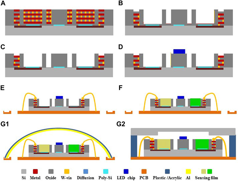
FIGURE 3. Fabrication process steps: (A) CMOS chip fabricated by the TSMC, (B) metal wet etching to define structures on the sensing chip, (C) RIE etching to remove the dielectric layer to open bonding pads for wire bonding, (D) assembly of the blue LED chip on the CMOS-MEMS chip, (E) wire bonding between the CMOS-MEMS chip and the PCB board, (F) dispensing of gas sensing films, and (G) bonding of light reflectors to cover the CMOS-MEMS chip.
Figure 4 shows micrographs of a typical fabricated sensing chip. The optical micrograph in Figure 4A displays the chip fabricated by the CMOS processes of TSMC. The scanning electron microscopy (SEM) micrograph in Figure 4B depicts the sensing chip after the post-CMOS metal wet etching. The inset zoom-in micrographs, respectively, show the cavity and the RTD routing at the bottom of the cavity. The SEM micrograph in Figure 4C exhibits the sensing chip with the blue LED bonded at the center stage. The micrograph in Figure 4D indicates the sensing chip with sensing materials dispensed in the cavity. The left micrograph in Figure 4E shows the hemispherical shell of different diameters prepared using the 3D printer, and the right micrograph in Figure 4E depicts the hemispherical shell coated with metal film for the light reflector. The flat plate reflector is shown in Figure 4F. Figure 5 shows a typical packaged sensing chip as the device under test (DUT). As displayed in the left micrograph of Figure 5A, alignment marks on the PCB were exploited to ensure the sensing chip was placed at the right location. The ventilation holes and circular groove on the PCB are, respectively, used to input the test gases and to mount the hemispherical shell optical reflector. The right micrograph in Figure 5A shows that both the sensing chip and the blue LED are electrically connected to the PCB by wire bonding. Micrographs in Figure 5B show the on/off states of the blue LED after the sensing chip is covered with the hemispherical shell optical reflector (20 mm in diameter). Micrographs in Figure 5C show the on/off states of the blue LED after the sensing chip is covered with the flat plate optical reflector (acrylic as the spacer). To show the operation of blue LED, parts of the optical reflectors were removed. In this study, the footprints of the sensing chip and the blue LED are, respectively, 2.48 × 2.68 mm2 and 890 × 890 μm2. The dimension of the circular groove in Figures 5A,B needs to match with the size of the hemispherical shell optical reflector.
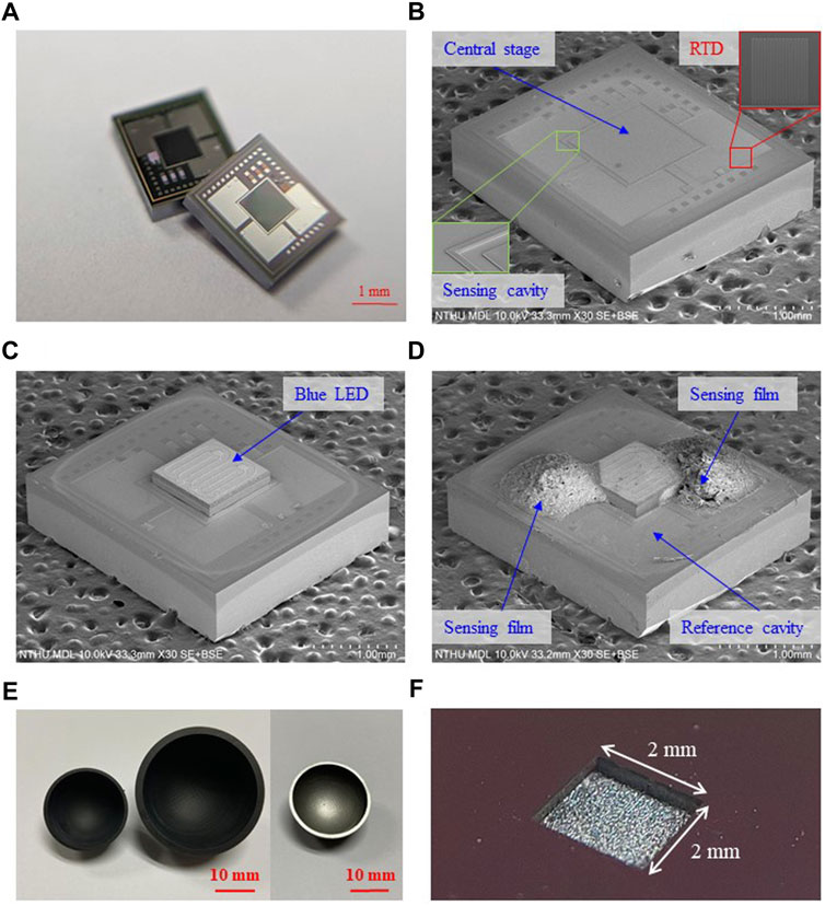
FIGURE 4. Micrographs to exhibit the typical fabrication and assembly results, (A) the CMOS chip fabricated by the TSMC, (B) the gas sensing chip fabricated after the post-CMOS processes, and the RTD and sensing cavity are shown in the inset zoom-in SEM micrographs, (C) the gas sensing chip bonded with the blue LED, (D) the gas sensing chip after the dispensing of sensing materials, (E) the 3D-printed polymer hemispherical shells and after being coated with metal film as the reflector, and (F) the micromachined Si flat plate reflector.
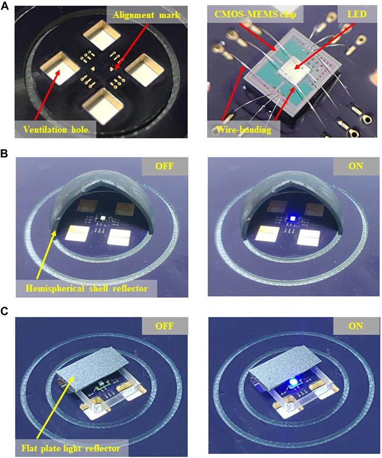
FIGURE 5. (A) Typical fabrication results of the gas sensor before/after wire bonding and assembly on the PCB, with the circular groove designed to align and mount the hemispherical shell reflector, (B) lighting test on the gas sensor with the hemispherical shell reflector, and (C) lighting test on the gas sensor with the flat plate reflector.
Finally, the sensing materials were prepared using the standard sol-gel process. The precursor of sol-gel is tetraethyl orthosilicate (TEOS). As shown in Figure 6A, after dissolving TEOS in ethanol (solvent), ammonia was added to form the porous silica (Rao et al., 2005). Finally, the sensing materials were coated on the surface of the silica particles. The micrograph depicts the porous silica prepared by the sol-gel process. The diameter of these silica particles is near 100 nm. In order to obtain material sensitive to O2, the silica was coated with C30H24Cl2N6Ru·6H2O so that λexc and λemi were, respectively, 470 and 610 nm (Jorge et al., 2004). Moreover, the silica coated with C16H7Na3O10S3 was prepared for CO2 detection, and λexc and λemi were, respectively, 460 and 520 nm (Nivens et al., 2002). Thermal analysis was performed to confirm that the sensing material was properly coated on the silica surface. In this test, the temperature range is 30°C–1,000°C and has a rising rate of 10°C/min. Measurements in Figures 6B,C and Figures 6D,E, respectively, show the thermogravimetric analysis (TGA) and the differential scanning calorimetry (DSC) analysis. According to TGA measurements in Figure 6B, the silica pyrolysis temperature changes from 581.4 °C to 584.3°C after the silica was coated with the O2 sensing material. Moreover, TGA measurements in Figure 6C indicate the silica pyrolysis temperature changes from 581.4 °C to 553.6°C after the silica was coated with the CO2 sensing material. The drift of silica pyrolysis temperature demonstrates that a force is generated between the sensing material and silica (Jaroniec et al., 1997) (Wu et al., 2020). Note that different sensing materials will generate intramolecular or intermolecular forces (Wu et al., 2020). For instance, the O2 sensing material (ionic compound) will generate an ionic bond force with the silica surface. The CO2 sensing material (molecular compound) will generate van der Waals forces and H-bonding with the silica surface. According to DSC measurements in Figure 6D, the energy peak of the silica drifts from 581.8 °C to 584.5°C after the silica was mixed with the O2 sensing material. DSC measurements in Figure 6E depict the energy peak of silica drifts from 581.8 °C to 553.3°C after the silica was mixed with the CO2 sensing material. These drifts are also caused by previously mentioned forces on the material (Jaroniec et al., 1997) (Wu et al., 2020). Since these two sensing materials have different bonding conditions with the silica surface, their energy peak drifts are also different. As a result, measurements show that the fluorescent materials have been coated onto the surface of silica effectively.
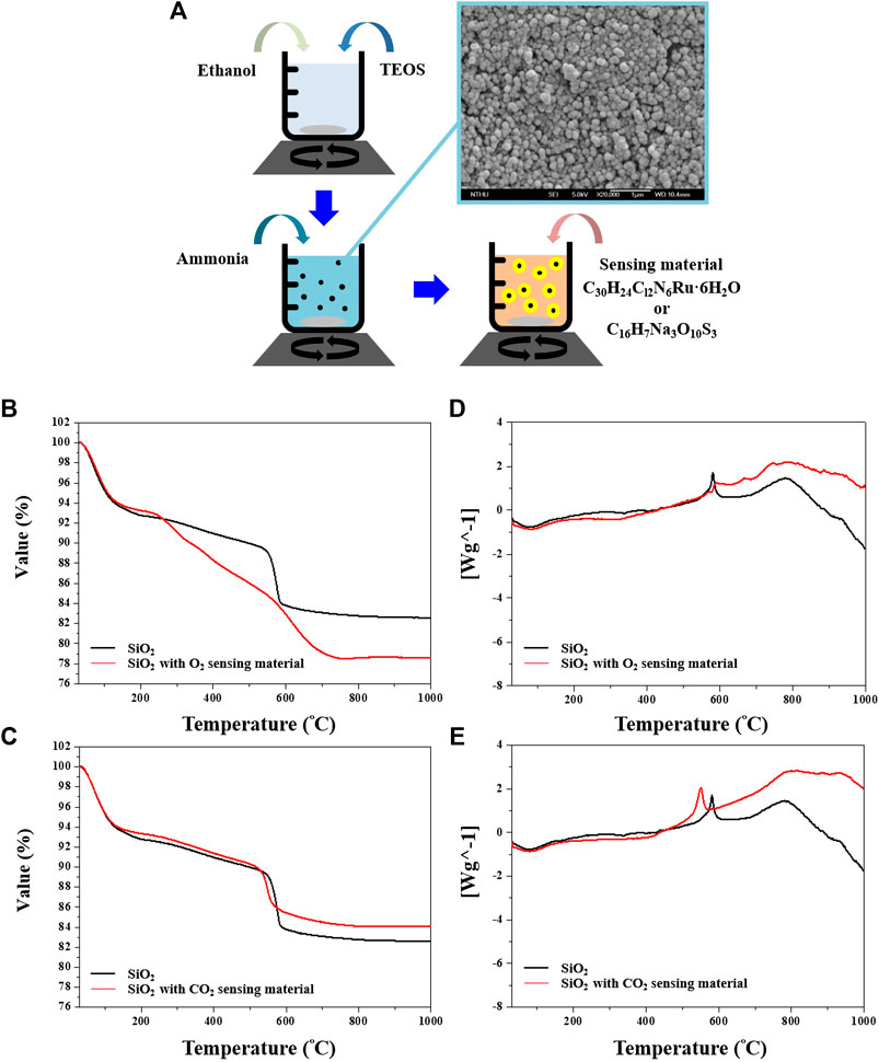
FIGURE 6. Fabrication and characterization of sensing materials: (A) sensing film fabrication process steps and SEM micrographs of sol-gel/silica, (B,C) TGA thermogram results, respectively, for O2 and CO2 sensing materials with silica, and (D,E) DSC thermogram results, respectively, for O2 and CO2 sensing materials with silica.
This study performed measurements to evaluate the sensing performances of the O2 and CO2 sensors with and without optical reflectors. Moreover, the temperature influence of the proposed gas sensor has also been characterized and investigated. Firstly, this study established the measurement setup in Figure 7A to characterize the RTD temperature sensing unit. The temperature controller under the fabricated sensing chip is used to specify a constant ambient temperature (at the range of 30°C–120°C) for testing. The source meter is used to measure the resistance of the RTD. Measurements in Figure 7B show the variation of resistance change with the ambient temperature. The results indicate that the sensitivity of the temperature is 0.07%/°C at the temperature range of 30°C–120°C. Secondly, the characteristics of the blue LED and photo-sensor used in this study are characterized. The spectrometer is employed to measure the wavelength of the LED. Typical measurement results in Figure 8A show that the central wavelength of LED is 452 nm. The overall emission wavelength covers the λexc (470/460 nm) of the sensing material. Thus, this commercially available blue LED fulfills the requirements in this study. Measurements in Figure 8B present the relationship between the reference photo-sensor (photo-sensor at the reference cavity) output current I0 and the LED driving current at room temperature for gas sensors with and without an optical reflector. The input current of the LED ranges from 10 to 250 mA. The results indicate that, for a given output current I0 from the reference photo-sensor (160 μA), the gas sensor without an optical reflector needs a higher input current (100 mA) on the LED, as compared with those for the gas sensor with optical reflectors (20 mA for the flat plate reflector and 70 mA for the hemispherical shell reflector). In other words, the power consumption of the presented sensors can be reduced by adding the light reflector.
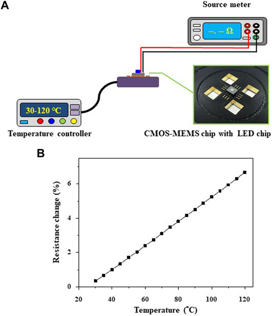
FIGURE 7. (A) Experimental setup for the calibration of the RTD temperature sensor, and (B) measured resistance change versus temperature.
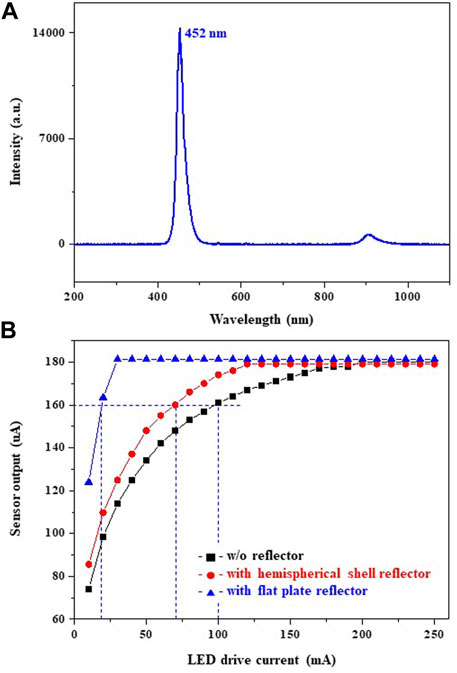
FIGURE 8. (A) Blue LED light spectral response, and (B) the output current from photo-sensors of three different gas sensor designs varying with the driving current on the LED chip.
The test setup in Figure 9 is established to characterize the performance of O2/CO2 sensors at different gas concentrations. The specimen is prepared and tested inside an opaque chamber with a standard O2, CO2, and N2 gas analyzer. The mass flow controllers (MFCs) are employed to control the gas flow and further control the gas concentration. The LED is driven through a constant current source from a power supply. The source meters are employed to measure output currents from the sensing chip at different O2/CO2 gas concentrations. Measurements in Figure 10 show the variation of the output current with gas concentrations for sensors with and without optical reflectors. Note that, based on the results in Figure 8B, this study specified the same I0 for each gas sensor during tests. Thus, the input currents of the LED for gas sensors of three different designs are, respectively, 20 mA (with a flat plate reflector), 70 mA (with a hemispherical shell reflector), and 100 mA (without a reflector). In addition, tests were performed under the humidity condition of 60%–65% RH and room temperature. Measurements indicate that the increase of gas concentration will enhance the fluorescence quenching reaction, so as to decrease the fluorescence intensity. As depicted in Figure 10A, the sensitivities of O2 gas concentration sensing (within the O2 gas concentration range of 14%–50%) are 0.12 μA/% (O2/N2) and 0.24 μA/% (O2/N2), respectively, for sensors with hemispherical shell and flat plate optical reflectors. The sensitivity for the design without an optical reflector is only 0.023 μA/% (O2/N2). Moreover, as shown in Figure 10B, the sensitivities of CO2 gas concentration sensing (within the CO2 gas concentration range of 14%–50%) are 0.19 μA/% (CO2/N2) and 0.32 μA/% (CO2/N2), respectively, for sensors with the hemispherical shell and the flat plate optical reflectors. The sensitivity for the design without an optical reflector drops to 0.12 μA/% (CO2/N2). The results indicate, even when each sensor was normalized at the same I0 during tests (i.e., LED on the gas sensor without a reflector provides much higher light emission), the designs with optical reflectors still have much higher sensitivities. The redirect of the light from the LED by the reflector could be the reason for such sensitivity enhancements. As reported in Coppel et al. (2015), the incidence angle of the light source could change the intensity of the detected fluorescence. Measurements in Figure 11 exhibit the responses of the gas sensor at different ambient temperatures (−25°C–−60°C). As the ambient temperature increases, the response and sensitivity of the gas sensor decreases. For example, the sensitivities of the CO2 sensor are 0.19 μA/% and 0.18 μA/%, respectively, at 25°C and 60°C. Thus, a monolithically integrated RTD temperature sensor can be exploited for temperature compensation. Measurements in Figure 12A indicate that O2 gas was injected into the test chamber at t = 0 s (the background gas is N2) to cause the fluorescence quenching of the O2 sensor, and the induced current If’ of the O2 sensing unit is dropped. However, the induced current of the CO2 sensing unit remained the same. The results show that the presented CO2 sensor has no crosstalk with the O2 gas. Moreover, measurements in Figure 12B demonstrate that the presented O2 sensor has no crosstalk with the CO2 gas. In summary, comparisons of the presented CMOS-MEMS gas sensor with other existing optical gas sensing devices are summarized in Table 1.
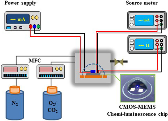
FIGURE 9. Experimental setup for gas sensing tests.
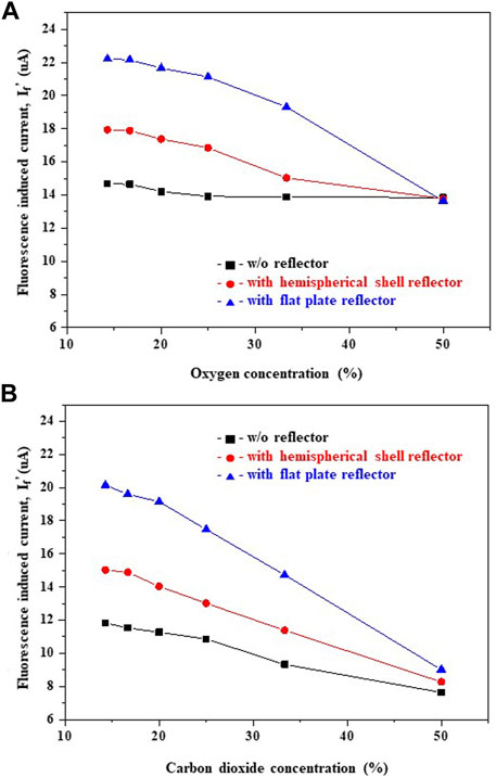
FIGURE 10. Responses for gas sensors of three different designs: (A) fluorescence-induced photo-currents If detected by gas sensors under different O2 concentrations, and (B) fluorescence-induced photo-currents If detected by gas sensors under different CO2 concentrations.
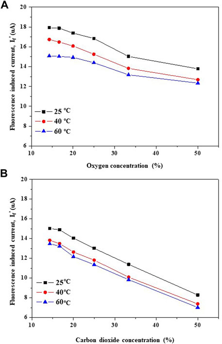
FIGURE 11. (A) Responses of the O2 sensors under different temperatures, and (B) responses of the CO2 sensors under different temperatures.
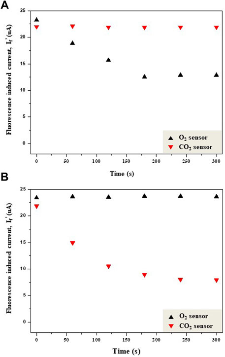
FIGURE 12. Crosstalk measurements of the presented sensor; the responses of O2 and CO2 sensing units when injecting (A) O2 gas, and (B) CO2 gas, into the test chamber.
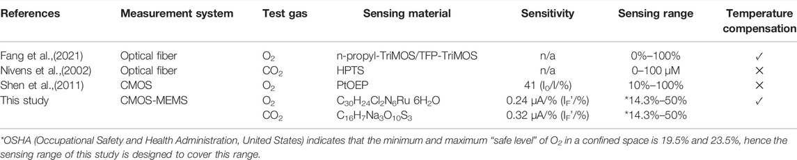
TABLE 1. Comparison of presented CMOS-MEMS optical gas sensors with existing optical-based gas sensors.
In this work, micro fluorescence quenching gas sensors comprised of a CMOS-MEMS sensing chip, LED chip, optical reflector, and sensing materials are designed and implemented. By using the TSMC standard CMOS and the in-house post-CMOS processes, the mechanical structures, temperature sensor, and photo-sensors are fabricated and monolithically integrated on the CMOS-MEMS sensing chip. The LED chip is selected to provide the required wavelength for sensing. The optical reflector can reflect and redirect the light emitted from the blue LED to the sensing cavity, which can effectively reduce the power consumption and can also improve the sensitivity. The vertically integrated temperature sensor on the gas sensor enables on-site temperature monitoring for sensing signal compensation. The O2 and CO2 gas sensors are implemented and tested to demonstrate the feasibility of the presented designs. The sensing materials are, respectively, mixed with C30H24Cl2N6Ru·6H2O and C16H7Na3O10S3 for O2 and CO2 detection. Moreover, two different light reflectors are, respectively, demonstrated using the micromachined Si flat plate and the 3D-printed polymer hemispherical shell. Note that the roughness of the reflector will cause the diffusion of the reflected light, and such an issue could be improved by using other processing methods such as injection molding. Measurements indicate that the designs with an optical reflector (hemispherical shell and flat plate) show an enhancement in sensitivity for sensor detection and also provide the benefit of lower power consumption for the LED. In addition, the flat plate reflector has a better performance (0.24 μA/% in O2/N2 and 0.32μA/% in CO2/N2) compared with the design with the hemispherical shell optical reflector (0.12 μA/% in O2/N2 and 0.19 μA/% in CO2/N2). In conclusion, the presented heterogeneous integration of CMOS-MEMS and LED chips could effectively reduce the size of optical gas sensors. The performance and power consumption of the optical gas sensor can be further improved by using the light reflector.
The original contributions presented in the study are included in the article/Supplementary Material, further inquiries can be directed to the corresponding author.
Y-CL and WF contributed to conception and design of the study. C-SL and CT performed the simulation analysis. YC and T-LC validated and analyzed data. All authors contributed to manuscript revision and read and approved the submitted version.
This research was sponsored in part by the Ministry of Science and Technology of Taiwan under grants MOST 110-2218-E-007-032, MOST 110–2923-E-007-009, and MOST 110–2926-I-007-506.
The authors declare that the research was conducted in the absence of any commercial or financial relationships that could be construed as a potential conflict of interest.
All claims expressed in this article are solely those of the authors and do not necessarily represent those of their affiliated organizations, or those of the publisher, the editors, and the reviewers. Any product that may be evaluated in this article, or claim that may be made by its manufacturer, is not guaranteed or endorsed by the publisher.
The authors want to thank the TSMC and the Taiwan Semiconductor Research Institute (TSRI), Taiwan, for supporting CMOS chip manufacturing. The authors also would like to thank the Center for Nanotechnology, Materials Science, and Microsystems (CNMM) of National Tsing Hua University for providing the process tool.
Arsat, R., Breedon, M., Shafiei, M., Spizziri, P. G., Gilje, S., Kaner, R. B., et al. (2009). Graphene-like Nano-Sheets for Surface Acoustic Wave Gas Sensor Applications. Chem. Phys. Lett. 467, 344–347. doi:10.1016/j.cplett.2008.11.039
Bartlett, P. N., and Guerin, S. (2003). A Micromachined Calorimetric Gas Sensor: an Application of Electrodeposited Nanostructured Palladium for the Detection of Combustible Gases. Anal. Chem. 75, 126–132. doi:10.1021/ac026141w
Chang, Y., Hasan, D., Dong, B., Wei, J., Ma, Y., Zhou, G., et al. (2018). All-Dielectric Surface-Enhanced Infrared Absorption-Based Gas Sensor Using Guided Resonance. ACS Appl. Mat. Interfaces 10, 38272–38279. doi:10.1021/acsami.8b16623
Chien, T.-L., Lee, Y.-C., Chou, T., Lin, Y.-Y., Chen, H.-Y., and Fang, W. (2022). “Fabrication and Integration of Soc Environment Sensing Hub with Gas/Pressure/Temperature Sensors,” in 2022 IEEE 35th International Conference on Micro Electro Mechanical Systems Conference (MEMS), 138–141. doi:10.1109/mems51670.2022.9699821
Chu, C.-S., and Lo, Y.-L. (2008). A Plastic Optical Fiber Sensor for the Dual Sensing of Temperature and Oxygen. IEEE Phot. Technol. Lett. 20, 63–65. doi:10.1109/lpt.2007.912568
Chu, Y., Chen, C., and Tsou, C. (2015). A Silicon-Based LED Packaging Substrate with an Island Structure for Phosphor Encapsulation Shaping. IEEE Trans. Compon. Packag. Manufact. Technol. 5, 155–162. doi:10.1109/tcpmt.2014.2379255
Coppel, L. G., Johansson, N., and Neuman, M. (2015). Angular Dependence of Fluorescence from Turbid Media. Opt. Express 23, 19552–19564. doi:10.1364/oe.23.019552
Fang, W., Li, S.-S., Chiu, Y., and Li, M.-H. (2021). 3D and Circuit Integration of MEMS. 1st Ed. Berlin, Germany: Wiley VCH.
Gas Sensor Applications (2021). CO2Meter. Available at https://www.co2meter.com/blogs/news/gas-sensor-applications.
Jaroniec, C. P., Gilpin, R. K., and Jaroniec, M. (1997). Adsorption and Thermogravimetric Studies of Silica-Based Amide Bonded Phases. J. Phys. Chem. B 101, 6861–6866. doi:10.1021/jp964002a
Jorge, P. A. S., Caldas, P., Rosa, C. C., Oliva, A. G., and Santos, J. L. (2004). Optical Fiber Probes for Fluorescence Based Oxygen Sensing. Sensors Actuators B Chem. 103, 290–299. doi:10.1016/j.snb.2004.04.086
Lee, Y.-C., Cheng, S.-W., Cheng, C.-L., and Fang, W. (2017). “Design and Implementation of Gas Sensor Array Based on Fluorescence Quenching Detection Using CMOS-MEMS Process,” in 2017 19th International Conference on Solid-State Sensors, Actuators and Microsystems (Transducers), 672–675. doi:10.1109/transducers.2017.7994138
Lee, Y.-C., Cheng, S.-W., and Fang, W. (2019). “Monolithic Integrated CMOS-MEMS Fluorescence Quenching Gas Sensor and Resistive Temperature Detector (RTD) for Temperature Compensation,” in 2019 20th International Conference on Solid-State Sensors, Actuators and Microsystems & Eurosensors XXXIII (Transducers & Eurosensors XXXIII), 1293–1296. doi:10.1109/transducers.2019.8808639
Lee, Y.-C., Hsieh, M.-L., Lin, P.-S., Yang, C.-H., Yeh, S.-K., Do, T. T., et al. (2021). CMOS-MEMS Technologies for the Applications of Environment Sensors and Environment Sensing Hubs. J. Micromechanics Microengineering 31, 074004. doi:10.1088/1361-6439/ac0514
Lee, Y.-C., Lin, S.-W., Liou, C.-S., Tsou, C., and Fang, W. (2021). “A CMOS-MEMS Fluorescence Quenching Gas Sensor Encapsulated with Silicon-Based LED Reflector,” in 2021 21st International Conference on Solid-State Sensors, Actuators and Microsystems (Transducers), 783–786. doi:10.1109/transducers50396.2021.9495443
Lin, Y.-C., Hong, P.-H., Yeh, S.-K., Chang, C.-C., and Fang, W. (2020). “Monolithic Integration of Pressure/Humidity/Temperature Sensors for CMOS-Mems Environmental Sensing Hub with Structure Designs for Performances Enhancement,” in 2020 IEEE 33rd International Conference on Micro Electro Mechanical Systems (MEMS), 54–57. doi:10.1109/mems46641.2020.9056401
Liou, C., and Tsou, C. (2018). Compact Dual-LED Packaging with a 3-D Free-form Lens for Uniform Rectangular Illumination. IEEE Trans. Compon. Packag. Manufact. Technol. 8, 578–587. doi:10.1109/tcpmt.2017.2781279
McDonagh, C., Bowe, P., Mongey, K., and MacCraith, B. D. (2002). Characterisation of Porosity and Sensor Response Times of Sol-Gel-Derived Thin Films for Oxygen Sensor Applications. J. Non-Crystalline Solids 306, 138–148. doi:10.1016/s0022-3093(02)01154-7
Nivens, D., Schiza, M. V., and Angel, S. M. (2002). Multilayer Sol-Gel Membranes for Optical Sensing Applications: Single Layer pH and Dual Layer CO2 and NH3 Sensors. Talanta 58, 543–550. doi:10.1016/s0039-9140(02)00323-5
Olson, J. M., Friedman, D. J., and Kurtz, S. (2003). “High-Efficiency III-V Multijunction Solar Cells,” in Handbook of Photovoltaic Science and Engineering. Editors Antonio Luque, and Steven Hegedus (Orlando, Fla: Academic Press).
Paul, A., Muthukumar, S., and Prasad, S. (2020). Review—Room-Temperature Ionic Liquids for Electrochemical Application with Special Focus on Gas Sensors. J. Electrochem. Soc. 167, 037511. doi:10.1149/2.0112003jes
Rao, K. S., El-Hami, K., Kodaki, T., Matsushige, K., and Makino, K. (2005). A Novel Method for Synthesis of Silica Nanoparticles. J. Colloid Interface Sci. 289, 125–131. doi:10.1016/j.jcis.2005.02.019
Shen, L., Ratterman, M., Klotzkin, D., and Papautsky, I. (2011). A CMOS Optical Detection System for Point-Of-Use Luminescent Oxygen Sensing. Sensors Actuators B Chem. 155, 430–435. doi:10.1016/j.snb.2011.01.001
SST Sensing Ltd (2021). How Is Gas Sensing Used in Transportation? Available at https://sstsensing.com/how-is-gas-sensing-used-in-transportation/.
Tsai, M.-H., Sun, C.-M., Liu, Y.-C., Wang, C., and Fang, W. (2009). Design and Application of a Metal Wet-Etching Post-process for the Improvement of CMOS-MEMS Capacitive Sensors. J. Micromechanics Microengineering 19 (7), 105017. doi:10.1088/0960-1317/19/10/105017
Tzeng, T.-H., Kuo, C.-Y., Wang, S.-Y., Huang, P.-K., Huang, Y.-M., Hsieh, W.-C., et al. (2016). A Portable Micro Gas Chromatography System for Lung Cancer Associated Volatile Organic Compound Detection. IEEE J. Solid-State Circuits 51, 259–272.
Wan, H., Yin, H., Lin, L., Zeng, X., and Mason, A. J. (2018). Miniaturized Planar Room Temperature Ionic Liquid Electrochemical Gas Sensor for Rapid Multiple Gas Pollutants Monitoring. Sensors Actuators B Chem. 255, 638–646. doi:10.1016/j.snb.2017.08.109
Wang, Y., Chen, W., Wang, P., Dai, S., Li, J., Li, Y., et al. (2021). Ultra-high-power-confinement-factor Integrated Mid-infrared Gas Sensor Based on the Suspended Slot Chalcogenide Glass Waveguide. Sensors Actuators B Chem. 347, 130466.
Keywords: CMOS-MEMS, environment sensor, gas sensor, fluorescence quenching, encapsulate
Citation: Lee Y-C, Liou C-S, Chien T-L, Tsou C and Fang W (2022) Integration and Encapsulation of Light-Emitting Diode and CMOS-MEMS Chips for Fluorescence Quenching Gas Sensor. Front. Mech. Eng 8:894060. doi: 10.3389/fmech.2022.894060
Received: 11 March 2022; Accepted: 14 April 2022;
Published: 17 May 2022.
Edited by:
Arantxa Uranga, Universitat Autònoma de Barcelona, SpainReviewed by:
Wei Xu, Shenzhen University, ChinaCopyright © 2022 Lee, Liou, Chien, Tsou and Fang. This is an open-access article distributed under the terms of the Creative Commons Attribution License (CC BY). The use, distribution or reproduction in other forums is permitted, provided the original author(s) and the copyright owner(s) are credited and that the original publication in this journal is cited, in accordance with accepted academic practice. No use, distribution or reproduction is permitted which does not comply with these terms.
*Correspondence: Weileun Fang, ZmFuZ0BwbWUubnRodS5lZHUudHc=
Disclaimer: All claims expressed in this article are solely those of the authors and do not necessarily represent those of their affiliated organizations, or those of the publisher, the editors and the reviewers. Any product that may be evaluated in this article or claim that may be made by its manufacturer is not guaranteed or endorsed by the publisher.
Research integrity at Frontiers
Learn more about the work of our research integrity team to safeguard the quality of each article we publish.