 Yi Chiu
 Cheng-Yen Lin2
 Hao-Chiao Hong
95% of researchers rate our articles as excellent or good
Learn more about the work of our research integrity team to safeguard the quality of each article we publish.
Find out more
ORIGINAL RESEARCH article
Front. Mech. Eng. , 12 May 2022
Sec. Micro- and Nanoelectromechanical Systems
Volume 8 - 2022 | https://doi.org/10.3389/fmech.2022.876714
This article is part of the Research Topic Design and Analysis of CMOS-MEMS Transducers View all 9 articles
MEMS accelerometers have been widely used in various applications with a wide range of signal levels and bandwidth. Therefore it is desired to have a sensor whose characteristics such as sensitivity and bandwidth can be reconfigured/tuned depending on specific applications. This paper presents a reconfigurable/tunable z-axis accelerometer whose mechanical resonant frequency, sensitivity and sensing bandwidth can be tuned by the electrostatic spring softening effect. The proposed accelerometer was designed using a commercial 0.35 μm CMOS foundry service. The tuning electrodes were implemented in the metal and polysilicon layers in the standard CMOS process. An on-chip chopper stabilized readout circuit was designed to convert the capacitance signal to a voltage readout. The sensing structure was released by post-CMOS wet metal etching. Measurement results showed the proposed accelerometer had a sensitivity of 12 mV/g in the range of 0–5 g. The sensitivity and bandwidth tuning ranges are 50% and 18%, respectively, for an applied tuning voltage of 25 V. The demonstrated device is the first reconfigurable/tunable CMOS-MEMS accelerometer in the literature to our best knowledge.
MEMS accelerometers have been widely used in various applications such as automotives, consumer electronics, industrial sensing, and health monitoring. The signal bandwidth in these applications varies significantly, as shown in Table 1. For example, the acceleration frequency range in automotive application is up to 400 Hz (Yazdi et al., 1998). In human activity monitoring, the acceleration signals are typically sampled at 25–40 Hz (Mathie et al., 2001; Bulling et al., 2014). For physiological signals, the normal respiration rate is 0.1–0.5 Hz (Morillo et al., 2010) while the cardiac signals has a bandwidth of 5–35 Hz (Kwon et al., 2011). Accelerometers are also used to measure heart sound between 20 and 500 Hz (Hu and Xu, 2012). Therefore it is desired to have a sensor whose characteristics such as the bandwidth and sensitivity can be reconfigured/tuned depending on the requirements from specific applications.
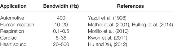
TABLE 1. Signal bandwidth for accelerometer applications.
Tunable MEMS accelerometers have been demonstrated over the past years. Most tunable accelerometers use electrostatic force to tune the effective spring constants in the device. For example, SOI technology was employed to implement an in-plane tunable resonant accelerometer where back-to-back tuning electrodes were used to enhance the sensitivity via the electrostatic spring softening effect (Xiong et al., 2021). For a bias voltage of 67 V, the sensitivity was increased from 492 Hz/g to 2,277 Hz/g in static tests. In (Daeichin et al., 2019), a two-layer polysilicon surface micromachining process was employed to fabricate a torsional out-of-plane accelerometer. In contrast to the more commonly used electrostatic attractive force, electrostatic repulsive force due to a bias voltage of 40–60 V was used in this device to tune its resonance frequency and sensitivity without suffering from the pull-in effect. In (Fain et al., 2018), a standard MEMS fabrication process was used to fabricate an in-plane rotational accelerometer. The tuning voltage up to 4.5 V was applied to the seismic mass through a RC network to control the sensing bandwidth. The resulting electromechanical torque effectively changed the quality factor and inertia in the equation of the motion of the sensor.
The tuning electrode configuration in tunable accelerometers based on the spring softening effect can be roughly divided into two categories: comb fingers for in-plane movement/sensing (Park et al., 1999; Zotov et al., 2015; Ding et al., 2017) and parallel-plate electrodes for out-of-plane movement/sensing (Lee et al., 2000; Caspani et al., 2014). In (Guo et al., 2021), both comb fingers and parallel-plate capacitors were used to control the in-plane stiffness-tunable accelerometer. As will be discussed in the following sections, the tunability and tuning voltage of electrostatic tuning are closely related to the gaps of the tuning electrodes. The smaller the gaps, the lower the tuning voltage and the easier the accelerometers can be tuned. For comb fingers, the vertical gaps are typically defined by photolithography and etching processes. In contrast, the gaps in parallel-plate electrodes are the thickness of deposited thin films if the gaps are formed by removing the sacrificial layers. Even though these parameters depend on specific device design and fabrication processes, the parallel-plate electrodes adopted in this study would have potentially smaller gaps and better tuning characteristics than the comb finger electrodes.
Design and fabrication of MEMS sensors using commercial CMOS foundry services enable on-chip integration with front-end readout circuits to reduce the effects of parasitics and noises and improve the sensor performance. The integration of sensors and readout circuits on a single chip can also help reduce the overall packaging and manufacturing cost. Such integrated CMOS-MEMS sensors have been demonstrated in accelerometers (Lemkin and Boser, 1999; Jiangfeng Wu et al., 2004; Hongwei Qu et al., 2008; Tan et al., 2011; Tsai et al., 2012; Chiu et al., 2013; Chiu et al., 2014; Chiu et al., 2016; Chiu et al., 2017; Chiu et al., 2019), gyroscopes (Jiang et al., 2000; Xie and Fedder, 2001; Sun et al., 2011), pressure sensors (Jang and Yun, 2017; Liao et al., 2021), inclinometers (Chiu et al., 2015), mass sensors (Verd et al., 2008; Wei and Lu, 2012), humidity sensors (Dai, 2007; Lazarus et al., 2010) and flow sensors (Liao et al., 2013). In addition to reducing noise and amplifying signals, the on-chip circuitry can also be used to drive actuators for feedback control and self testing (Lemkin and Boser, 1999). Among these integrated sensors, accelerometers have been under intensive studies. However, tunability has not been demonstrated in integrated CMOS-MEMS accelerometers to the best of our knowledge.
This paper presents a reconfigurable/tunable z-axis accelerometer implemented with the CMOS-MEMS technology. The mechanical resonant frequency and thus the sensing bandwidth and sensitivity can be tuned by the electrostatic softening effect. The proposed sensor was designed using a commercial 0.35 μm CMOS foundry service. The tuning electrodes were implemented in the metal2 (M2) and polysilicon layers in the standard CMOS process. The sensing structure was released by post-CMOS wet metal etching. In the device design, the sub-micron tuning gap formed by removing the metal1 (M1) layer in the CMOS process allows low tuning voltage and good tunability. An on-chip chopper stabilized readout circuit was designed to convert the capacitance signal to a voltage readout and reduce the effects of parasitics and noises.
An accelerometer can be modeled as a second-order spring-mass-damper system. As shown in Figure 1A, the equation of motion of a conventional micro accelerometer is
where a is the acceleration to be measured, z is the displacement of the shuttle mass, m is the mass, b is the damping constant, and km is the mechanical spring constant. Under a harmonic excitation at angular frequency ω, the above equation can be written as
where A and Z are the amplitudes of acceleration and displacement, respectively, ω0 = (km/m)1/2 is the resonance frequency, and Q = mω0/b is the quality factor. Eq. (2) is in fact the mechanical sensitivity of the accelerometer Sm. For quasi-static operation, the signal frequency ω is much lower than the resonance frequency ω0. Thus the accelerometer sensitivity Sm can be approximated as
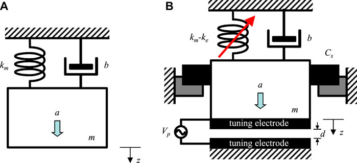
FIGURE 1. Operation principles of (A) conventional micro accelerometer and (B) proposed reconfigurable/tunable accelerometer.
The above equation shows there is a trade-off between the sensitivity and the bandwidth of a conventional accelerometer, and both parameters are pre-determined by the mechanical design of the device. For tunable accelerometers whose characteristics such as bandwidth and sensitivity can be controlled by an external signal, the spring constant is typical used as the tuning parameter since the mass is difficult to change. As shown in Figure 1B of the proposed tunable accelerometer, a pair of tuning electrodes is added to the bottom of the shuttle mass to tune the total spring constant and thus the resonance frequency of the device. When a tuning voltage Vp is applied to the tuning electrodes, an electrostatic force Fe is generated,
where
where the negative spring constant
The resonance frequency and thus the sensing bandwidth and sensitivity can be tuned by Vp according to specific application requirements. In Eqs 5, 6, the spring softening effect is inversely proportional to d3. Therefore, devices with small tuning gap d, such as the proposed device in this study, will have potentially low tuning voltage and good tunability.
The sensing structures of the proposed accelerometer, including the shuttle mass, suspension springs and sensing electrodes, were implemented in the back-end-of-line (BEOL) metal and oxide stacks in a standard 0.35 μm CMOS process that offers two polysilicon layers and four metal layers. The tuning electrodes were implemented in the metal and polysilicon layers. The sensing capacitances Cs in Figure 1B are out-of-plane comb finger capacitances. An on-chip chopper stabilized readout circuit was designed to convert the capacitance change to a voltage signal.
The schematic top view of the proposed accelerometer is shown in Figure 2A. The shuttle mass of 315 × 315 μm2 area is suspended by four springs. Comb fingers are used for capacitive sensing. Etching holes of 10 × 10 μm2 area and spaced by 15 μm are designed to facilitate the post-CMOS release etching. The meander springs have a width of 3 μm and segment length of 118 μm. The total thickness of the structure is 5.73 μm, as shown in Figure 2B. Among the multiple metal layers in the CMOS process, only the M2 layer is used in the shuttle mass and springs for signal routing. The mass, spring constants, and resonance frequencies obtained by theoretical calculation and finite-element-method (FEM) simulation by using Coventorware are summarized in Table 2.
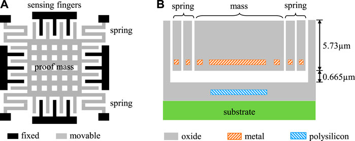
FIGURE 2. (A) Top view and (B) cross sectional view of proposed accelerometer.
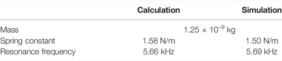
TABLE 2. Device design parameters.
As shown in Figure 2B, the tuning electrodes are implemented in the M2 and Poly1 layers. The electrodes are covered by 1 μm thick SiO2 and have a gap of 0.665 μm. The dielectric constant of SiO2 is 3.9, therefore the effective gap deff between the metal electrodes is 1.18 μm. The pull-in voltage VPI for the tuning electrodes can found as.
The small pull-in voltage, enabled by the small tuning gap, indicates typical CMOS circuits can be used to control and tune the characteristics of the sensor. Figure 3 shows the FEM simulation of the electrode displacement vs the applied tuning voltage Vp. The smaller pull-in voltage (∼0.85 V) found in the simulation is attributed to the fringing effect of the edges of the etching holes that contributes extra effective area to the electrode area S.
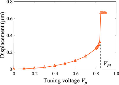
FIGURE 3. Pull-in voltage simulation.
The sensing capacitors are vertical differential capacitors proposed in (Xie and Fedder, 2000). As shown in Figure 4, the M2-M4 layers in the fixed comb fingers are connected by vias to be the common electrodes. The common electrodes form a pair of differential capacitors Ctop and Cbottom between the M4 and M2 electrodes in the moveable electrodes, respectively. In the proposed accelerometer, the gap between the comb fingers electrodes is 1.5 μm. The overlap length between the fingers is 90 μm. From the FEM simulation, the total sensing capacitance at rest is 234 fF and the capacitance sensitivities of the accelerometer are 1.9 fF/g and 2.8 fF/g for Ctop and Cbottom, respectively.
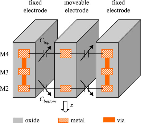
FIGURE 4. Differential sensing capacitors.
An on-chip chopper stabilized circuit was integrated with the sensor to convert the capacitance signal to a voltage output (Lemkin and Boser, 1999; Jiangfeng Wu et al., 2004). The chopper stabilized circuit can reduce the effect of noise and improve the signal-to-noise ratio and resolution of the sensor. The circuit was designed and implemented with a 3.3 V supply voltage. Figure 5A shows the overall schematic of the integrated readout circuit in this work. Four differential sensing capacitors form a fully differential capacitive bridge. The capacitive signals ±ΔC are modulated by the high frequency carriers
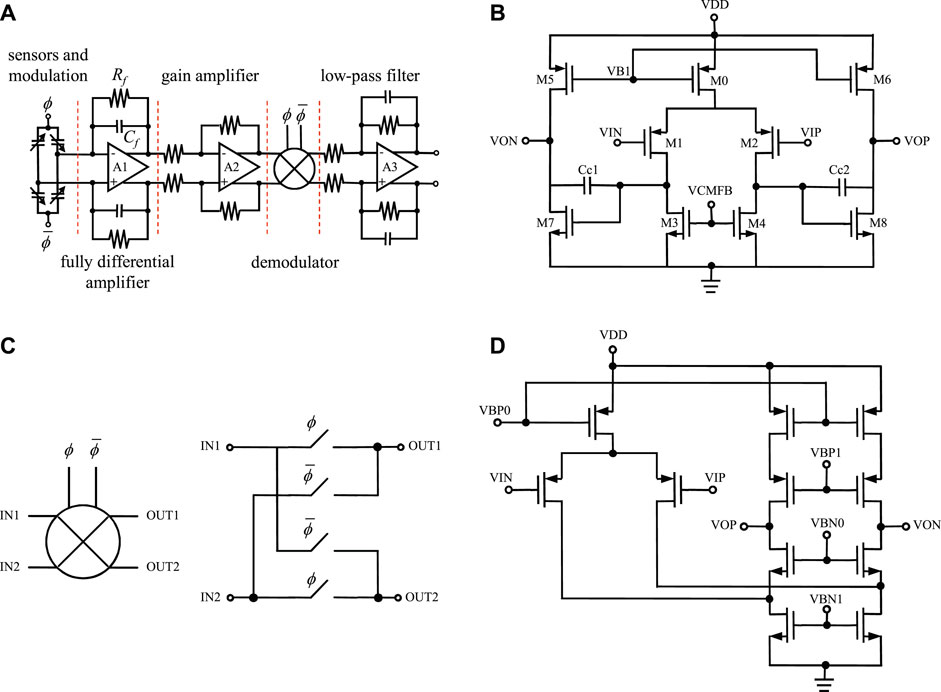
FIGURE 5. Schematics of (A) on-chip chopper stabilized readout circuit, (B) fully differential amplifiers A1 and A2, (C) demodulator, (D) fully differential folded cascode amplifier A3.
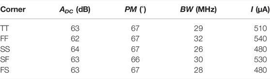
TABLE 3. Simulated characteristics of the two-stage fully differential amplifier in this work.
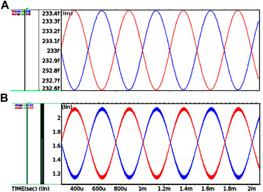
FIGURE 6. Simulation of readout circuit, (A) input signal, (B) demodulated output signal.
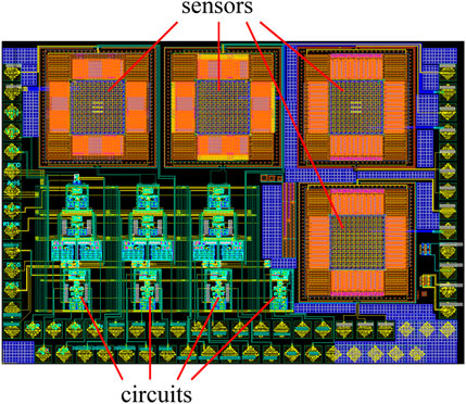
FIGURE 7. Chip layout.
After the chip was fabricated and delivered by the foundry, post-CMOS processes were carried out to release the sensing structure. Various mechanical, electrical, and acceleration tests of the sensor are discussed in the following sections.
Figure 8 shows the process flow of the post-CMOS release process. As shown in Figure 8A, the passivation above the vertical etching paths was removed in the CMOS fab. The as-received chip was immersed in the metal etchant H2SO4+H2O2 (3:1) at 100 °C for 1.5 h to etch the aluminium metal and tungsten via in the etching paths and the M1 sacrificial layer. This process released the movable structure and formed the tuning gap, as shown in Figure 8B. A laser cutting system was used to remove the passivation and expose the contact pads for wire bonding (Figure 8B). Figure 9A shows the scanning electron microscope (SEM) view of the released device. Figure 9B shows a focused ion beam (FIB) cut at the center of the proof mass, showing a gap of 11.8 μm between the proof mass and the substrate surface. The released device was then mounted on a piezoelectric actuator and tested for mechanical resonance by laser Doppler vibrometry. Figure 10 shows a resonance frequency of 10.6 kHz and indicates the device was successfully released.
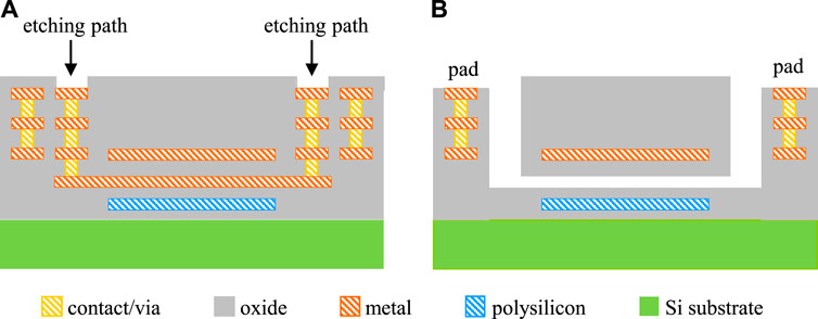
FIGURE 8. Post-CMOS release process, (A) as-received chip, (B) after wet metal etching and laser pad opening.
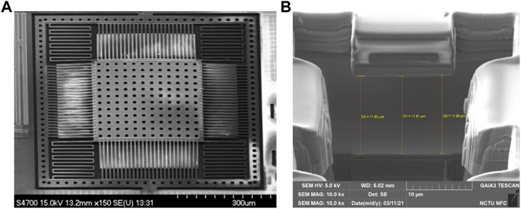
FIGURE 9. Released device, (A) SEM micrograph, (B) FIB cut.
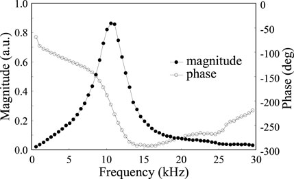
FIGURE 10. Mechanical resonance test.
In acceleration tests, static and dynamic accelerations were applied to the proposed sensor and the signals from the readout sensing circuits were observed. The integrated sensor chip was mounted on a printed circuit board (PCB) with other passive electronic components and connectors for testing. The test board and sensing circuits were powered by a Keithley 2,400 source meter. A Tektronix AFG 3102 function generator was used to supply the chopping/modulation signal. The output signals were observed and recorded with a Rohde and Schwarz RTO 1004 oscilloscope. The data sampling frequency fs was set at 4.5 kHz in the oscilloscope. In static acceleration tests, the test PCB was mounted on a rotation stage and rotated various angles θ with respect the earth gravity. The component of the earth gravity projected on the sensing axis was used as the static acceleration input
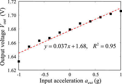
FIGURE 11. Static acceleration test.
In dynamic acceleration tests, the test board was mounted on a Modal Shop 2007E shaker controlled by the Tektronix AFG3102 function generator. The built-in waveform generator in a Keysight DSOX1102G oscilloscope and a PiezoDrive PDX150 amplifier were used to supply the tuning voltage Vp to tune the mechanical resonance frequency of the sensor. A commercial accelerometer (PCB Piezotronics 352C65) was mounted on the shaker to monitor and calibrate the vibration magnitude. The test parameters in the dynamic acceleration tests include the frequency of the acceleration fin, the amplitude of the acceleration aext, and the tuning voltage Vp. Figure 12 shows the outputs from the proposed accelerometer and the commercial accelerometer in a typical experiment. It can be seen that their waveforms match each other quite well. This verifies both the sensor and the sensing circuit were functioning properly.
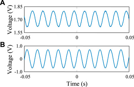
FIGURE 12. Measured output signal waveforms of (A) proposed accelerometer and (B) commercial accelerometer for fin = 100 Hz, aext = 5 grms and Vp = 0 V.
In dynamic tests, a sinusoidal acceleration was applied and the AC output Vout from the sensing circuits was captured by the oscilloscope. The recorded data were processed with Fast Fourier Transform (FFT) to find the corresponding signal strength as well as various harmonics, interferences, and noise components in the frequency domain. Figure 13A shows the measured sensor output Vout for various input acceleration. The measured sensitivity is about 12 mV/g. Figure 13B shows the power spectral density obtained by FFT for aext = 1 grms and fin = 100 Hz. The peak at the excitation frequency 100 Hz is the signal tone; the peaks at multiple excitation frequencies (200 Hz, 300 Hz, etc.) are distortion harmonics; and the peaks at multiples of the 60 Hz power line frequencies are power noise. By excluding the harmonics and power line noise, the noise floor can be calculated as 3.1 mg/rtHz.
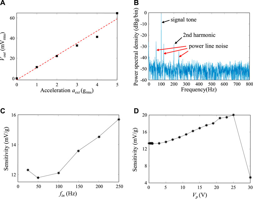
FIGURE 13. Dynamic acceleration test results, (A) Vout vs aext for fin = 100 Hz and Vp = 0 V, (B) output power spectral density for aext = 1 grms, fin = 100 Hz and Vp = 0 V, (C) sensitivity for aext = 5 grms and Vp = 0 V, (D) reconfigurability/tunability test for aext = 5 grms and fin = 100 Hz.
The sensor was also subjected to accelerations at various frequencies and the output is shown in Figure 13C. While remaining relatively constant, the sensitivity does increase slightly in the range of test frequency up to 250 Hz. It was later found that the PCB on which the sensor chip, circuit components and connectors were mounted had a resonance frequency of about 600 Hz. Therefore the PCB resonance can interfere with the tests and cause the apparent increase of sensitivity.
The reconfigurability/tunability of the proposed sensor was verified by applying a tuning voltage Vp to the tuning electrodes while keeping the other test parameters constant. The applied voltage causes the spring softening effect which reduces the total spring constant and increases the sensitivity, according to Eq. 3. As shown in Figure 13D, the sensitivity increases with the applied voltage Vp and has a sudden drop when the applied voltage is above 30 V. The sensitivity drop is attributed to the pull-in effect because the movable shuttle mass is snapped to the substrate by the electrostatic force and can no longer respond to the inertial force due to the external acceleration. For the applied tuning voltage up to 25 V in Figure 13D, the sensitivity tuning range is about 50% and implies a bandwidth tuning range of 18%.
There are certain discrepancies between the characteristics from measurement and design. The possible causes are discussed in the following. The proposed accelerometer was designed based on the nominal process data such as the material properties and thickness of various metal and oxide layers disclosed by the CMOS manufacturing foundry. However, it is known that these BEOL thin films have residual stress that can cause the released MEMS structures to deform. The characteristics of the deformed device will then deviate from the original design. Generally speaking, devices with larger dimensions and more compliant structures, such as inertial sensors, are prone to larger deformation and related reliability problems in the presence of residual stress. On the other hand, devices with smaller dimensions or more rigid anchoring constraints, such as resonators or pressure sensors, tend to have less deformation and more reproducible characteristics. The residual stress in the deposited films in CMOS processes has been studied in the literature (Yen et al., 2011; Cheng et al., 2015; Tsai et al., 2015; Valle et al., 2017; Valle et al., 2021) but has not been well characterized and controlled in the fab. This is one of the reasons that pure monolithic CMOS MEMS devices are rare in the commercial products.
The accelerometer proposed in this study has a 315 × 315 μm2 proof mass which is suspended by four springs. The tuning gap underneath the square proof mass is designed to be 0.665 μm, which is the thickness of the sacrificial M1 layer. However, as shown in Figure 9B, the gap between the release structure and the bottom tuning electrode can be as larger as 11.8 μm. Figure 14A further shows the white light interferometric measurement of the surface topology of a released device. Figure 14B is a line scan of the surface height through the center of the proof mass. It can be seen that the suspended proof mass is warped and elevated from the surface of the chip by up to about 13 μm, agreeing with the results from the FIB experiment. The raised structure and enlarged gap have several effects on the device performance:
1. The movable and fixed sensing fingers will no longer level with each other in the z axis as shown in Figure 4. Thus the sensing capacitance C0 can be reduced and the differential capacitance signal ±ΔC may not work as expected. This is potentially the main reason why the measured sensitivity is much smaller than the designed value.
2. Since the tuning gap increases from less than 1 μm in the original design to more than 10 μm in the measured device, the pull-in voltage VPI and thus the tuning voltage Vp will be increased significantly. The pull-in voltage estimated in Eq. 7 based on the ideal gap of 0.665 μm is about 1.0 V. If the gap is increased to 12 μm but the other device parameters remain ideal, the pull-in voltage will increase to about 47 V, which is close to the measured value.
3. In addition to the enlarged tuning gap, the residual stress and/or the post-CMOS release process may cause non-uniform deformation. As shown in Figure 14C, while the proof mass is successfully released and suspended, the free ends of the springs bend down toward the substrate surface. If any of the free ends of the meander springs touches and sticks to the substrate, the effective spring constant will increase and possibly cause the measured resonance frequency (10.6 kHz) in Figure 10 to be higher than the simulation value (5.7 kHz) in Table 2. The increased resonance frequency also contributes to the reduction of sensitivity.
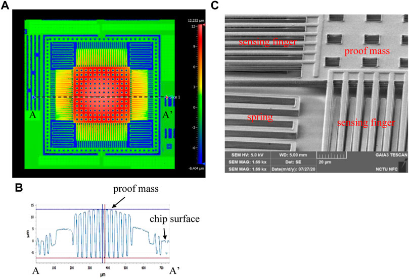
FIGURE 14. (A) White light interferometric measurement of the surface topology of a released device, (B) line scan of surface height through AA′, (C) SEM view of suspended proof mass and bent down spring.
The stress-induced deformation in CMOS MEMS devices with various BEOL metal layers and metal-oxide stacking structures have been studied in (Cheng et al., 2015; Tsai et al., 2015; Yen et al., 2011; Valle et al., 2017; Valle et al., 2021). However, it is known from the literature and our own experience that the residual stress and induced deformation is difficult to control and reproduce. The effect of stress induced deformation on the performance of capacitive CMOS-MEMS accelerometers can be alleviated by curl matching frames (Xie and Fedder, 2000), which were adopted in the proposed device. In the thermomechanical simulation in the device design, proof mass deformation similar to the measured result in Figure 14 was observed, but the deformed movable and fixed sensing fingers remained leveled to each other relatively well thanks to the matching frame. In the actual released device in Figures 9, 14, however, the height difference between the two sets of fingers are 3–5 μm, which is much higher than expected from simulation. Since the residual stress in CMOS processes is difficult to control and predict, this issue needs to be tackled from other aspects. From the structural design point of view, Tsai et al. proposed a pure-oxide design, instead of the conventional metal oxide stacking design, to reduce the thermal deformation (Tsai et al., 2015). In the current proposed accelerometer, a planar metal layer was used for the tuning electrode. Thus the pure oxide proof mass design in (Tsai et al., 2015) is not applicable. However, the metal tuning electrode in the current device can be replaced with the Ti/TiN electrode as demonstrated in (Chen et al., 2019) in the future work. The proof mass will be composed of a thick oxide layer (4–5 μm) and a much thinner Ti/TiN electrode (0.14 μm) in the bottom. Thus the oxide proof mass will remain less deformed in the presence of stress from the thin electrode layer. In addition, the thermal expansion coefficients of various materials in the BOEL layers are 0.5, 23, 8.6, 9–10 ppm/K for SiO2, Al, Ti, and TiN, respectively. Therefore the thermal mismatch can also be reduced in the Ti/TiN electrode design compared with the current Al electrode design. Yen et al. showed thick and symmetric metal-oxide stacking realized by wet oxide etching can be used to significantly reduce the deformation in the presence of residual stress (Yen et al., 2011). Such structural design and post-CMOS processing will also be considered in future design to alleviate the stress-induced deformation. It is noted that all the suspended structures, including the proof mass, sensing fingers, and curl matching frames, need to be designed with the same layer stacking in order to compensate for any residual stress that can not be fully predicted in the design phase.
The performance of the proposed reconfigurable/tunable CMOS-MEMS capacitive accelerometer is compared with other integrated CMOS-MEMS capacitive accelerometers in the literature, as shown in Table 4. Even though the stress-induced deformation has deteriorated the performance of the proposed device, its reconfigurability/tunability is clearly demonstrated.
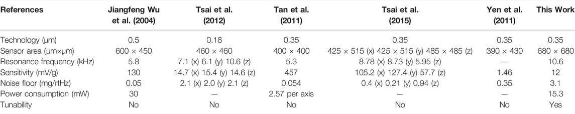
TABLE 4. Performance comparison.
This paper presents a reconfigurable/tunable z-axis accelerometer based on the electrostatic spring softening effect. The proposed monolithic accelerometer and on-chip readout circuits were implemented by using a commercial 0.35 μm 2P4M CMOS foundry service. The tuning electrodes were designed in the metal and polysilicon layers in the BEOL CMOS process. The sensing structure was released by post-CMOS wet metal etching. Measurement results showed the proposed accelerometer had a sensitivity of 12 mV/g in the range of 0–5 g. The sensitivity and bandwidth tuning ranges are 50% and 18%, respectively, for an applied tuning voltage of 25 V. The measured characteristics deviated from the design values due to severe residual stress induced structural deformation.
The raw data supporting the conclusions of this article will be made available by the authors, without undue reservation.
YC initiated the idea, supervised the MEMS design, and prepared the manuscript. H-CH supervised the circuit design. C-YL was in charge of device design, post-CMOS fabrication, experiments, and data analysis.
This work was supported in part by the Ministry of Science and Technology, Taiwan, ROC, under Grants MOST 109-2221-E-009–037-MY2, MOST 110–2221-E-A49-071-MY2, MOST 110–2221-E-A49-151-MY2.
The authors declare that the research was conducted in the absence of any commercial or financial relationships that could be construed as a potential conflict of interest.
All claims expressed in this article are solely those of the authors and do not necessarily represent those of their affiliated organizations, or those of the publisher, the editors and the reviewers. Any product that may be evaluated in this article, or claim that may be made by its manufacturer, is not guaranteed or endorsed by the publisher.
The authors acknowledge the support of the National Center for High-performance Computing, the Taiwan Semiconductor Research Institute, and the National Yang Ming Chiao Tung University Nano Facility Center, Taiwan, R.O.C., for various simulation, fabrication, and characterization tools.
Bulling, A., Blanke, U., and Schiele, B. (2014). A Tutorial on Human Activity Recognition Using Body-Worn Inertial Sensors. ACM Comput. Surv. 46, 1–33. doi:10.1145/2499621
Caspani, A., Comi, C., Corigliano, A., Langfelder, G., Zega, V., and Zerbini, S. (2014). Dynamic Nonlinear Behavior of Torsional Resonators in MEMS. J. Micromech. Microeng. 24 (9), 095025. doi:10.1088/0960-1317/24/9/095025
Chen, C.-Y., Li, M.-H., Zope, A. A., and Li, S.-S. (2019). A CMOS-Integrated MEMS Platform for Frequency Stable Resonators-Part I: Fabrication, Implementation, and Characterization. J. Microelectromech. Syst. 28 (5), 744–754. doi:10.1109/JMEMS.2019.2936149
Cheng, C.-L., Tsai, M.-H., and Fang, W. (2015). Determining the Thermal Expansion Coefficient of Thin Films for a CMOS MEMS Process Using Test Cantilevers. J. Micromech. Microeng. 25 (2), 025014. doi:10.1088/0960-1317/25/2/025014
Chiu, Y., Chen, B.-T., and Hong, H.-C. (2015). “Integrated CMOS MEMS Liquid Capacitive Inclinometer,” in Proceedings of the 18th International Conference on Solid-State Sensors, Actuators and Microsystems (Transducers), Anchorage, AK, USA, 21-25 June 2015 (IEEE), 1152–1155. doi:10.1109/Transducers.2015.7181132
Chiu, Y., Hong, H.-C., and Chang, C.-M. (2017). “Three-axis CMOS MEMS Inductive Accelerometer with Novel Z-axis Sensing Scheme,” in Proceedings of the 19th International Conference on Solid-State Sensors, Actuators and Microsystems (Transducers), Kaohsiung, Taiwan, 18-22 June 2017 (IEEE), 410–413. doi:10.1109/Transducers.2017.7994074
Chiu, Y., Hong, H.-C., and Lin, C.-W. (2016). “Inductive CMOS MEMS Accelerometer with Integrated Variable Inductors,” in Proceedings of the 29th IEEE International Conference on Micro Electro Mechanical Systems (MEMS), Shanghai, China, 24-28 June 2016 (IEEE), 974–977. doi:10.1109/MEMSYS.2016.7421795
Chiu, Y., Hong, H.-C., and Wu, P.-C. (2013). Development and Characterization of a CMOS-MEMS Accelerometer with Differential LC-Tank Oscillators. J. Microelectromech. Syst. 22 (6), 1285–1295. doi:10.1109/JMEMS.2013.2282419
Chiu, Y., Huang, T.-C., and Hong, H.-C. (2014). A Three-Axis Single-Proof-Mass CMOS-MEMS Piezoresistive Accelerometer with Frequency Outp. Sensors Mater. 26 (2), 95–108. doi:10.18494/SAM.2014.945
Chiu, Y., Liu, H.-W., and Hong, H.-C. (2019). A Robust Fully-Integrated Digital-Output Inductive CMOS-MEMS Accelerometer with Improved Inductor Quality Factor. Micromachines 10 (11), 792. doi:10.3390/mi10110792
Daeichin, M., Ozdogan, M., Towfighian, S., and Miles, R. (2019). Dynamic Response of a Tunable MEMS Accelerometer Based on Repulsive Force. Sensors Actuators A Phys. 289, 34–43. doi:10.1016/j.sna.2019.02.007
Dai, C.-L. (2007). A Capacitive Humidity Sensor Integrated with Micro Heater and Ring Oscillator Circuit Fabricated by CMOS-MEMS Technique. Sensors Actuators B Chem. 122 (2), 375–380. doi:10.1016/j.snb.2006.05.042
Ding, H., Wang, W., Ju, B.-F., and Xie, J. (2017). A MEMS Resonant Accelerometer with Sensitivity Enhancement and Adjustment Mechanisms. J. Micromech. Microeng. 27 (11), 115010. doi:10.1088/1361-6439/aa8d99
Fain, B., Souchon, F., Berthelot, A., Anciant, R., Robert, P., and Jourdan, G. (2018). Dynamic Control of an Accelerometer Bandwidth through Tunable Damping Factor and Effective Moment of Inertia. IEEE Micro Electro Mech. Syst. (MEMS) 2018, 948–951. doi:10.1109/MEMSYS.2018.8346714
Guo, Y., Ma, Z., Zhang, T., Zheng, X., and Jin, Z. (2021). A Stiffness-Tunable MEMS Accelerometer. J. Micromech. Microeng. 31 (2), 025005. doi:10.1088/1361-6439/abcedb
Hongwei Qu, H., Huikai Xie, D., and Xie, H. (2008). A Monolithic CMOS-MEMS 3-axis Accelerometer with a Low-Noise, Low-Power Dual-Chopper Amplifier. IEEE Sensors J. 8 (9), 1511–1518. doi:10.1109/JSEN.2008.923582
Hu, Y., and Xu, Y. (2012). “An Ultra-sensitive Wearable Accelerometer for Continuous Heart and Lung Sound Monitoring,” in Proceedings of the Annual International Conference of the IEEE Engineering in Medicine and Biology Society, San Diego, CA, USA, 28 Aguest 2012 (IEEE), 694–697. doi:10.1109/EMBC.2012.6346026
Jang, M., and Yun, K.-S. (2017). MEMS Capacitive Pressure Sensor Monolithically Integrated with CMOS Readout Circuit by Using Post CMOS Processes. Micro Nano Syst Lett 5 (4). doi:10.1186/s40486-016-0037-3
Jiang, X., Seeger, J. I., Kraft, M., and Boser, B. E. (2000). “A Monolithic Surface Micromachined Z-axis Gyroscope with Digital Output,” in Proceedings of the Symposium on VLSI Circuits, Honolulu, HI, USA, 15-17 June 2000 (IEEE), 16–19. doi:10.1109/VLSIC.2000.852839
Jiangfeng Wu, J., Fedder, G. K., and Carley, L. R. (2004). A Low-Noise Low-Offset Capacitive Sensing Amplifier for a 50-/spl Mu/g//spl radic/Hz Monolithic CMOS MEMS Accelerometer. IEEE J. Solid-State Circuits 39 (5), 722–730. doi:10.1109/JSSC.2004.826329
Kwon, S., Lee, J., Park, G. S., and Park, K. S. (2011). “Validation of Heart Rate Extraction through an iPhone Accelerometer,” in Proceedings of the Annual International Conference of the IEEE Engineering in Medicine and Biology Society, Boston, MA, USA, 30 Augest 2011 (IEEE), 5260–5263. doi:10.1109/IEMBS.2011.6091301
Lazarus, N., Bedair, S. S., Lo, C.-C., and Fedder, G. K. (2010). CMOS-MEMS Capacitive Humidity Sensor. J. Microelectromech. Syst. 19 (1), 183–191. doi:10.1109/JMEMS.2009.2036584
Lee, B.-L., Oh, C.-H., Lee, S., Chun, Y.-S., and Chun, K.-J. (2000). “A Vacuum Packaged Differential Resonant Accelerometer Using Gap Sensitive Electrostatic Stiffness Changing Effect,” in Proceedings of the 13th IEEE International Conference on Micro Electro Mechanical Systems (MEMS), Miyazaki, Japan, 23-27 January 2000 (IEEE), 352–357. doi:10.1109/MEMSYS.2000.838542
Lemkin, M., and Boser, B. E. (1999). A Three-axis Micromachined Accelerometer with a CMOS Position-Sense Interface and Digital Offset-Trim Electronics. IEEE J. Solid-State Circuits 34 (4), 456–468. doi:10.1109/4.753678
Liao, P.-W., Hong, H.-C., and Chiu, Y. (2021). “A CMOS-MEMS Capacitive Pressure Sensor with Differential Sensing Electrodes and On-Chip Frequency Output Circuits,” in Proceedings of the 21st International Conference on Solid-State Sensors, Actuators and Microsystems (Transducers), Orlando, FL, USA, 20-21 June 2021 (IEEE), 90–93. doi:10.1109/Transducers50396.2021.9495427
Liao, S.-H., Chen, W.-J., and Lu, M. S.-C. (2013). A Cmos Mems Capacitive Flow Sensor for Respiratory Monitoring. IEEE Sensors J. 13 (5), 1401–1402. doi:10.1109/JSEN.2013.2245320
Mathie, M. J., Basilakis, J., and Celler, B. G. (2001). “A System for Monitoring Posture and Physical Activity Using Accelerometers,” in Proceedings of the 23rd Annual International Conference of the IEEE Engineering in Medicine and Biology Society, Istanbul, Turkey, 25-28 October2001 (IEEE), 3654–3657. doi:10.1109/IEMBS.2001.1019627
Morillo, D. S., Ojeda, J. L. R., Foix, L. F. C., and Jimenez, A. L. (2010). An Accelerometer-Based Device for Sleep Apnea Screening. IEEE Trans. Inf. Technol. Biomed. 14 (2), 491–499. doi:10.1109/TITB.2009.2027231
Park, K.-Y., Lee, C.-W., Jang, H.-S., Oh, Y., and Ha, B. (1999). Capacitive Type Surface-Micromachined Silicon Accelerometer with Stiffness Tuning Capability. Sensors Actuators A Phys. 73, 109–116. doi:10.1016/S0924-4247(98)00262-3
Sun, H., Jia, K., Liu, X., Yan, G., Hsu, Y.-W., Fox, R. M., et al. (2011). A CMOS-MEMS Gyroscope Interface Circuit Design with High Gain and Low Temperature Dependence. IEEE Sensors J. 11 (11), 2740–2748. doi:10.1109/JSEN.2011.2158819
Tan, S.-S., Liu, C.-Y., Yeh, L.-K., Chiu, Y.-H., Lu, M. S.-C., and Hsu, K. Y. J. (2011). An Integrated Low-Noise Sensing Circuit with Efficient Bias Stabilization for CMOS MEMS Capacitive Accelerometers. IEEE Trans. Circuits Syst. I 58 (11), 2661–2672. doi:10.1109/TCSI.2011.2142990
Tsai, M.-H., Liu, Y.-C., and Fang, W. (2012). A Three-axis CMOS-MEMS Accelerometer Structure with Vertically Integrated Fully Differential Sensing Electrodes. J. Microelectromech. Syst. 21 (6), 1329–1337. doi:10.1109/JMEMS.2012.2205904
Tsai, M.-H., Liu, Y.-C., Liang, K.-C., and Fang, W. (2015). Monolithic CMOS-MEMS Pure Oxide Tri-axis Accelerometers for Temperature Stabilization and Performance Enhancement. J. Microelectromech. Syst. 24 (6), 1916–1927. doi:10.1109/JMEMS.2015.2452270
Valle, J., Fernandez, D., Gibrat, O., and Madrenas, J. (2021). Manufacturing Issues of BEOL CMOS-MEMS Devices. IEEE Access 9, 83149–83162. doi:10.1109/ACCESS.2021.3086867
Valle, J., Fernandez, D., Madrenas, J., and Barrachina, L. (2017). Curvature of BEOL Cantilevers in CMOS-MEMS Processes. J. Microelectromech. Syst. 26 (4), 895–909. doi:10.1109/JMEMS.2017.2695571
Verd, J., Uranga, A., Abadal, G., Teva, J. L., Torres, F., LÓpez, J., et al. (2008). Monolithic CMOS MEMS Oscillator Circuit for Sensing in the Attogram Range. IEEE Electron Device Lett. 29 (2), 146–148. doi:10.1109/LED.2007.914085
Wei, G.-C., and Lu, M. S.-C. (2012). Design and Characterization of a CMOS MEMS Capacitive Resonant Sensor Array. J. Micromechanics Microengineering 22 (12), 125030. doi:10.1088/0960-1317/22/12/125030
Xie, H., and Fedder, G. K. (2001). “A CMOS-MEMS Lateral-axis Gyroscope,” in Proceedings of the 14th IEEE International Conference on Micro Electro Mechanical Systems (MEMS), Interlaken, Switzerland, 25 June 2001 (IEEE), 162–165. doi:10.1109/MEMSYS.2001.906505
Xie, H., and Fedder, G. K. (2000). “A CMOS Z-axis Capacitive Accelerometer with Comb-Finger Sensing,” in Proceedings of the 13th IEEE International Conference on Micro Electro Mechanical Systems (MEMS), Miyazaki, Japan, 23-27 January 2000 (IEEE), 496–501. doi:10.1109/MEMSYS.2000.838567
Xiong, X., Zou, X., Wang, Z., Wang, K., Li, Z., and Yang, W. (2021). Using Electrostatic Spring Softening Effect to Enhance Sensitivity of MEMS Resonant Accelerometers. IEEE Sensors J. 21 (5), 5819–5827. doi:10.1109/JSEN.2020.3037700
Yazdi, N., Ayazi, F., and Najafi, K. (1998). Micromachined Inertial Sensors. Proc. IEEE 86 (8), 1640–1659. doi:10.1109/5.704269
Yen, T.-H., Tsai, M.-H., Chang, C.-I., Liu, Y.-C., Li, S.-S., Chen, R., et al. (2011). Improvement of CMOS-MEMS Accelerometer Using the Symmetric Layers Stacking Design. IEEE SENSORS 2011, 145–148. doi:10.1109/ICSENS.2011.6127150
Keywords: CMOS-MEMS, accelerometer, reconfigurable, tunable, spring softening, readout circuit
Citation: Chiu Y, Lin C-Y and Hong H-C (2022) A Monolithic CMOS-MEMS Reconfigurable/Tunable Capacitive Accelerometer with Integrated Sensing Circuits. Front. Mech. Eng 8:876714. doi: 10.3389/fmech.2022.876714
Received: 15 February 2022; Accepted: 19 April 2022;
Published: 12 May 2022.
Edited by:
Wei-Chang Li, National Taiwan University, TaiwanReviewed by:
Guo-Hua Feng, National Tsing Hua University, TaiwanCopyright © 2022 Chiu, Lin and Hong. This is an open-access article distributed under the terms of the Creative Commons Attribution License (CC BY). The use, distribution or reproduction in other forums is permitted, provided the original author(s) and the copyright owner(s) are credited and that the original publication in this journal is cited, in accordance with accepted academic practice. No use, distribution or reproduction is permitted which does not comply with these terms.
*Correspondence: Yi Chiu, eWljaGl1QG1haWwubmN0dS5lZHUudHc=
Disclaimer: All claims expressed in this article are solely those of the authors and do not necessarily represent those of their affiliated organizations, or those of the publisher, the editors and the reviewers. Any product that may be evaluated in this article or claim that may be made by its manufacturer is not guaranteed or endorsed by the publisher.
Research integrity at Frontiers
Learn more about the work of our research integrity team to safeguard the quality of each article we publish.