 Kawtar Belrhiti Alaoui
 Saida Laalioui1,2
 Abdelkader Outzourhit
95% of researchers rate our articles as excellent or good
Learn more about the work of our research integrity team to safeguard the quality of each article we publish.
Find out more
METHODS article
Front. Mech. Eng. , 23 November 2020
Sec. Micro- and Nanoelectromechanical Systems
Volume 6 - 2020 | https://doi.org/10.3389/fmech.2020.560385
This article is part of the Research Topic Nanofilms and Nanostructures for Energy Applications View all 6 articles
In this work, a detailed description of the various steps involved in the fabrication of high-efficiency hydrogenated amorphous-silicon cells using plasma-enhanced chemical vapor deposition, and a novel shadow masking technique is presented. The influence of the different masking methods on the cell parameters was experimentally investigated. Particularly, the short-circuit current density (Jsc), the fill factor, the open circuit voltage (Voc), and the resistive losses indicated by the shunt (Rsh) and series (Rs) resistances were measured in order to assess the performance of the cells as a function of the masks used during the cell fabrication process. The results indicate that the use of a masking technique where the p-i-n structure was first deposited over the whole surface of a 20 cm2 × 20 cm2 substrate, followed by the deposition, deposits the back contact through a metal mask, and by the ultrasonic soldering of indium to access the front contact is a good alternative to laser scribing in the laboratory scale. Indeed, a record efficiency of 8.8%, with a short-circuit current density (Jsc) of 15.6 mA/cm2, an open-circuit voltage (Voc) of 0.8 V, and a fill factor of 66.07% and low resistive losses were obtained by this technique. Furthermore, a spectroscopic ellipsometry investigation of the uniformity of the film properties (thickness, band gap, and refractive index) on large-area substrates, which is crucial to mini-module fabrication on a single substrate and for heterojunction development, was performed using the optimal cell deposition recipes. It was found that the relative variations of the band gap, thickness, and refractive index n are less than 1% suggesting that the samples are uniform over the 20 cm2 × 20 cm2 substrate area used in this work.
Hydrogenated amorphous-silicon (a-Si:H) is a very promising material which has drawn significant interest in several research fields, including in single-junction and tandem solar cells as an absorber, in silicon heterojunction cells as a passivation layer (Sai et al., 2018), in radiation detectors (Davis et al., 2020), optoelectronic and photonic devices (Chong et al., 2020), and as a photo-electrodes in water splitting powered by solar energy (Stuckelberger et al., 2017).
Shadow-masking techniques can be considered as a low-cost pattern generation and thin-film device fabrication technique (Park et al., 2006) compared to laser scribing. Indeed, hydrogenated amorphous silicon (a-Si:H) spot-size converters were fabricated using this simple technique (Lipka et al., 2008). However, a-Si:H solar cells fabricated by a classical masking method such as the hot-wire chemical vapor deposition technique showed an efficiency of only 6% (Nelson et al., 2001), which is much lower than the record of 10.3% obtained by solar cells deposited by PECVD (Lambertz et al., 2015). This record efficiency was obtained using the laser scribing technique, and the cell parameters were Voc of 0.89 V, Jsc of 17.20 mA/cm2, and a FF of 67.0% (Lambertz et al., 2015). Further improvement of the performance of solar cells obtained by the masking technique is therefore still possible.
On the other hand, the thickness and opto-electronic property uniformities play a decisive role in large-area thin-film devices. Indeed, the uniform deposition of the layers on the surface is absolutely required to develop efficient large-area thin-film modules (Hoetzel et al., 2016). In this regard, an efficiency of 6.4% was attained for 20 cm2 × 20 cm2 cells, with a fill factor (FF) of 0.59, a short-circuit current (Jsc) of 14.15 mA/cm2, and an open-circuit voltage (Voc) of 0.79 V (Ledermann et al., 2001). The proven uniformity of the various layers in this case was 2.5% (Ledermann et al., 2001), suggesting that further improvement is also possible in this case. Furthermore, a-Si:H plays a crucial role in heterojunction silicon solar cells as it is used as a passivation layer of the crystalline Si wafer and carrier selective (p and n-type layers). Recently, a record efficiency of 23.5% was reported in this family of cells (Dréon et al., 2020). In this case, also, thin-film uniformity over a large-area crystalline Si wafer is necessary.
In this work, we have used the cluster facility of GEP (Dréon et al., 2020; Green Energy Park Platform,) to fabricate a-Si:H thin films on large-area substrates using plasma-enhanced chemical vapor deposition (PECVD) at 13.56 MHz plasma excitation frequency on 20 cm2 × 20 cm2 glass substrates (Asahi-VU) coated with a fluorine-doped (SnO2:F) film (Belrhiti Alaoui et al., 2020). Solar cells with a 1 cm2 × 1 cm2 active area were defined by using different shadow masking methods instead of laser scribing, to investigate the influence of this method on the electrical characteristics of the obtained cells. The optimized deposition recipes of each layer were then used to deposit films on 20 cm2 × 20 cm2 borosilicate substrates to study sample uniformity for a potential up-scaling.
The deposition of intrinsic i-type a-Si:H, n-type a-Si:H, and p-type a-SiC:H was performed in separate plasma-enhanced chemical vapor deposition (PECVD) chambers for each layer at 13.56 MHz plasma excitation frequency. The Al back-contact, on the other hand, was deposited by rf-sputtering in another chamber. All of the four chambers were connected in one multi-chamber cassette cluster tool facility to ensure a chain deposition without vacuum breaking at the Green Energy Park (GEP) (Green Energy Park Platform,; Alaoui et al., 2015). The deposition parameters of the various layers are shown in Table 1. These parameters were obtained through an optimization process where the optical parameters of the films (optical band gap, refractive index, thickness) were measured by spectroscopic ellipsometry.
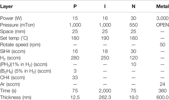
TABLE 1. Optimized recipes for the deposition of the a-Si:H layers of p-i-n cells.
Solar cell I-V curve measurements for the 1 cm2 × 1 cm2 cell fabricated by the masking technique described below were performed using a “QuickSun 130CA” solar simulator with an AM1.5 (1,000 W/m2) spectrum.
The sample uniformity on large-area substrates was examined through the measurements of the band gap (Eg), thickness, and refractive index n on different regions of the sample. These parameters were obtained by spectroscopic ellipsometry measurements performed using a Horiba SMART SE ellipsometer. The optimized deposition methods were used for this purpose for each layer.
Following the optimization process of the various layers, the methods detailed in Table 1 were for the fabrication of p-i-n solar cells. This was performed by the sequential deposition of the 10 nm p-type a-SiC:H on a textured SnO2:F (FTO) –coated Asahi Glass substrate with a sheet resistance of 10 Ω/square. This is followed by a 200 nm i-type a-Si:H absorber layer, and a 19 nm n-type a-Si:H layer. Solar cells with an active area of 1 cm2 × 1 cm2 were delimited by a combination of a Kapton tape mask (referred to as TM) and a metal mask (MM). In some cells, and as shown in Figure 1, the metal mask was used after the deposition of a complete p-i-n structure to deposit the Al back-contact (thickness 600 nm). In this case, access to the front SnO2:F contact was performed by ultrasonic soldering (U-SS) of indium through the various layers of the cell (Figures 1D and 2). The various steps involved in the fabrication of the best cells are schematically described in Figures 1 and 2.
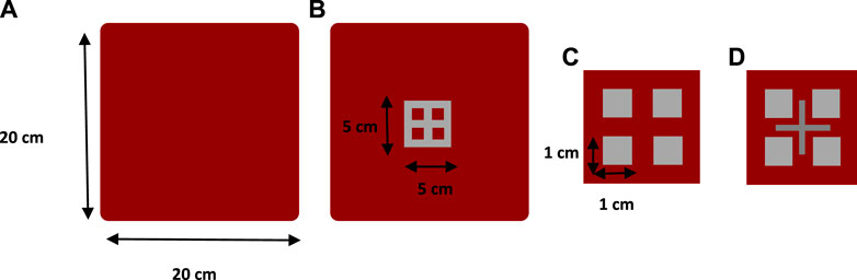
FIGURE 1. Top-down arrangement of the fabrication of a single junction cell: (A) deposition of the p-i-n structure on the 20 cm2 × 20 cm2 SnO2:F/glass substrates, (B) fixation of metal mask on the p-i-n structure and deposition of the Al back contact, (C) samples cutting, and (D) indium soldering to access to the front contact.
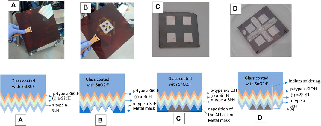
FIGURE 2. Side-view cross section and steps of the method of the fabrication of a single junction cell: (A) deposition of the p-i-n structure on the 20 cm2 × 20 cm2 SnO2:F/glass substrates, (B) fixation of the metal mask on the p-i-n structure, (C) deposition of the Al back contact, (D) samples cutting and indium soldering to access to the front contact.
Subsequently, the optimized deposition parameters for i-type a-Si:H, n-type a-Si:H, and p-type a-SiC:H, respectively were used to deposit these layers on large-area 20 cm2 × 20 cm2 borosilicate glass substrates in order to study the uniformity of the resulting films. The optimization of the deposition parameters was performed through a combination of ellipsometry measurements (optical parameters) combined with the performance of the fabricated p-i-n cells.
One of the objectives of the present work was to develop, compare, and test an effective shadow masking method that may be a good alternative to laser scribing on lab-scale research for the development of high quality solar cells using PECVD and PVD deposition techniques. To quantify the quality of fabricated films and the effect of the masking technique, p-i-n solar cells were fabricated. The cell performance parameters were then used as indicators of the quality of the various films and their interfaces. The objective was then to maximize single-junction p-i-n cell efficiency.
The parameters of the best solar cells obtained so far are presented in Table 2 for different masking techniques. The lowest efficiency in this series of cells is 4.8% obtained for cell 1 fabricated by using a metal mask throughout the deposition process of the p-i-n cell, i.e., the deposition of the p, i, and n-layers and the metal back-contact. The highest efficiency in this series of cells was 8.8%, which was obtained by using the second masking technique where the p-i-n structure was first deposited on the entire substrate, and then a metal mask was used to deposit the Al back contact. The Raman and impedance spectroscopy, the SEM image, and the optical parameters of this best cell were previously studied and reported in other work (Belrhiti Alaoui et al., 2020). Ultrasonic soldering of indium through the various layers was then used to access the front FTO contact. In this case, edge effects were significantly reduced. This second masking technique seemed to improve the efficiency significantly, as it can be observed by comparing the performance parameters of cell 1 and cells 4 to 6.
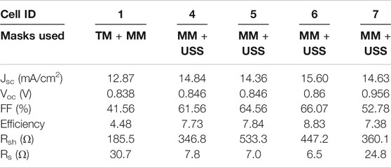
TABLE 2. Electrical parameters of the fabricated p-i-n solar cells using the different combinations of masks (TM: Kapton tape mask, MM: metal mask, and USS: ultrasonic soldering).
Figure 3 shows the typical current-voltage characteristics of the first cells fabricated by means of the simple masking techniques described above. As it can be clearly seen in this figure and in Table 2, the masking technique choice significantly affects the short-circuit current density (Jsc) and resistive losses as indicated by the shunt (Rsh) and series (Rs) resistances, and consequently the fill factor (FF). The Metal Mask + ultrasound soldering performances are clearly better than the conventional metal mask method. The open circuit voltage (Voc), on the other hand, was not significantly affected by the choice of the masking method. The series resistance was obtained from the inverse of the slope of the I-V curve under open circuit conditions, while the shunt resistance was found from the inverse of the slope of the I-V curve under the short circuit conditions.
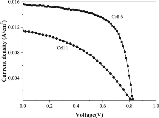
FIGURE 3. Typical I-V characteristic of the fabricated p-i-n solar cells for two different masking techniques (■ Metal Mask + ultrasound soldering; ● Metal mask)
A quick comparison of the characteristics of the cells shows that indium soldering reduces the series resistance (compare cell 1 and cell 6) while the masking technique affects the shunt resistance because of the edge effects (cells 1 and 6). The shunt resistance is much higher when the metal mask is used in the last step instead of using it from the beginning to delimit the cells during the deposition process. The cell that exhibits the highest efficiency is characterized by the highest short-circuit current and the lowest resistive losses and high FF.
Other factors such as the layer thickness of n and p were also investigated. The efficiency does not change significantly when the p-layer thickness is varied between 10 and 15 nm. Similarly, the cell efficiency changed slightly when the n-layer thickness was varied between 18 and 23 nm. On the other hand, when the thickness of the i-layer was increased from 196.7 nm (cell 5) to 262.3 nm (cell 6), the efficiency and Jsc increased because of an effective absorption of light. The optimal thickness of the i-layer is usually located between 260 and 300 nm. Furthermore, the addition of a 1–2 nm a-SiC:H buffer layer between the p- and i-layers slightly affected the cell parameters. A detailed investigation of these effects is however out of the scope of the present work.
In order to study the uniformity of the films on 20 cm2 × 20 cm2 glass substrates, the thickness, band-gap, and refractive index of the various a-Si:H layers were determined using spectroscopic ellipsometry on five regions: the center and the four corners of the rectangular glass substrates as shown in Figure 4. The uniformity is crucial for both large-area cells and for the development of mini-modules on a single substrate.
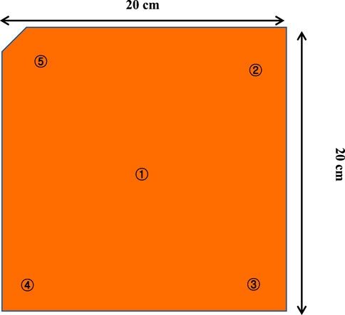
FIGURE 4. Spectroscopic ellipsometry measurements points.
The results of these tests are summarized in Table 3 which shows that the obtained optical parameters (Eg and n) are characteristic of the various layers and are in good agreement with the values reported in the literature. In addition, the parameters that quantify the sample uniformity, the mean value, the maximum deviation, which is the largest difference between the mean and the individual values, in addition to the standard deviation are shown in this table for the three types of a-Si:H.
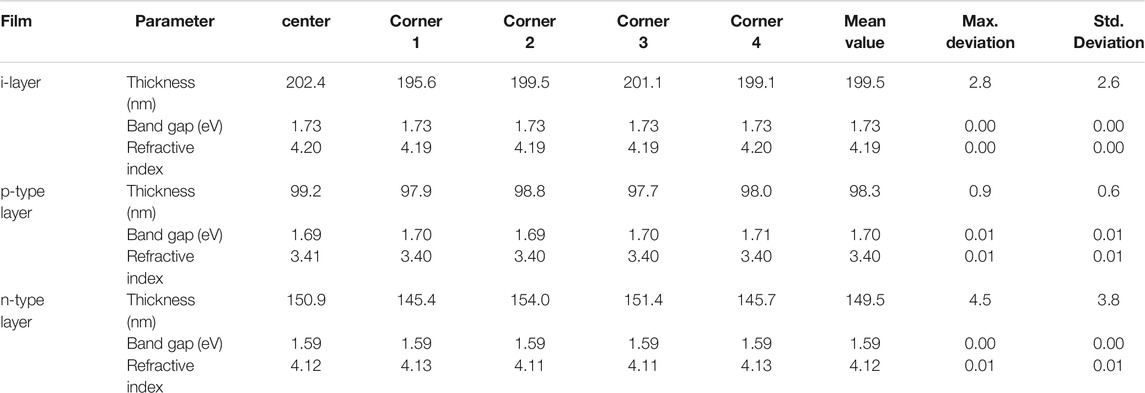
TABLE 3. Variation of the optical parameters and thickness of the i, p, and n a-Si:H layers deposited by PECVD across the surface of the 20 cm2 × 20 cm2 substrate.
In this work single-junction p-i-n a-Si:H cells were prepared and characterized for the first time using shadow masks. The combination between metal mask and ultrasonic soldering gave a good alternative in the absence of the laser scribing technique for lab-scale preparation of a-Si:H cells deposited by PECVD. As it can be seen from Table 2, the highest efficiency obtained in our laboratory using this simple masking technique is 8.86%, which is the highest efficiency obtained so far using this technique, with a Jsc of 15.6 mA/cm2, a Voc of 0.86V, an FF of 66.07%, and the lowest resistive losses. This efficiency is slightly lower than the world record in this type of cells (Lambertz et al., 2015). However, it should be noted that this record efficiency was obtained by limiting the cell by laser scribing, which effectively eliminates edge effects, instead of shadow masking which was used in this work.
Our results suggest that further improvements are possible, as Jsc can be improved. The lower efficiency may be attributed either to the parasitic absorption within the p-layer or to the slightly lower active layer thickness in our cells. Increasing the band gap of the p-layer will results in a higher built-in potential and allows more light to reach the absorber layer (i-layer). In addition, the p-layer should be thin enough to maximize its transparency but thick enough to generate an electric field in the intrinsic layer, which is crucial for the separation of the photo-generated carriers.
Increasing the i-layer thickness may increase Jsc and efficiency, as more photons will be absorbed. However, better stability of the cell usually requires the use of thinner intrinsic a-Si:H layers to increase the electric field strength across this active layer (Ramanujam and Verma, 2012). Similarly, the hydrogen contents of the film, a function of the dilution ratio and other process parameters, improves the quality of the i-layer, through the reduction of defect density, and leads to an increase in Jsc and Voc. Moreover, Jsc can also be enhanced by texturing the back contact as the scattering of the long wavelength arriving at this level will increase (Ramanujam and Verma, 2012; Meillaud et al., 2015; Stuckelberger et al., 2017; Fortes et al., 2018). All these effects will be further systematically investigated. In addition, the thin (1–4 nm) buffer layer between the p-layer and the intrinsic layer will also be optimized in order to accommodate the band offset between the two layers and to prevent the back diffusion of the photo-generated electrons into the p-type layer. Consequently, the effect of the following parameters on the performance of a single-junction a-Si:H solar cell will be further investigated: 1) the p-layer thickness and band gap, which affects the amount of light that enters the active layer. 2) The hydrogen dilution ratio, which affects the structure, the defect density, and the thickness of the active a-Si:H layer, and consequently the short-circuit current and the open-circuit voltage of the cell. 3) The TCO carrier collection layer, and 4) the Al back-reflector (BR) contact which will be replaced by Ag.
The uniformity of the film properties across the 20 cm2 × 20 cm2 substrate is excellent as demonstrated by ellipsometry measurements. As shown in Table 3, the relative variations of the three critical parameters (e.g., thickness, and refractive index n) are less than 1%, suggesting that the samples are very uniform over the 20 cm2 × 20 cm2 area. The results suggest that the developed recipes for i-type a-Si:H, n-type a-Si:H, and p-type a-SiC:H present a good potential for high-efficiency large-area a-Si:H solar cells. It should be noted that the uniformity of the layers involved in the p-i-n or in other cell configurations is crucial for both large-area cells and for the development of mini-modules on a single substrate (Ledermann et al., 2001; Hoetzel et al., 2016; Kim and Lee, 2018).
The next steps would be to engage in the fabrication of heterojunctions and multiple-junction tandem cells using the same shadow masking technique. In a further development, we will investigate the potential of the shadow mask technique for the large-scale deposition of p-i-n a-Si:H on 20 cm2 × 20 cm2 substrates, which will take advantage of the good sample uniformity to make a high efficiency 20 cm2 × 20 cm2 mini module.
In this work, we investigated the use of simple and low-cost masking techniques to make single-junction a-Si:H solar cells deposited by PECVD. It was found that the use of a metal mask in the last step of the cell fabrication process to deposit the Al back contact resulted in the highest efficiency of 8.8% compared with the other masking techniques. On the other hand, the uniformity of the different layers deposited on large-area substrates was found to be excellent as suggested by the relative variations of the critical film parameters (band gap, thickness, and refractive index) which did not exceed 1% over the 20 cm2 × 20 cm2 substrate.
The raw data supporting the conclusions of this article will be made available by the authors, without undue reservation.
KA conducts the deposition of the layer, data interpretation and the redaction of the article, her field of research is silicon thin films solar cells. SL helped on the deposition process, the data manipulation, member of the lab, her research field is perovskites for tandem solar cells, she will use the obtained efficient amorphous solar cell as a sub cell for the perovskite deposition. BI the manager of the research institute of IRESEN and the one who initiated the amorphous silicon research thematic is the project supervisor AO is the head of the LN2E Lab and the mentor in the research, he contributes on giving guidelines to this work, data interpretation and article correction.
The authors declare that the research was conducted in the absence of any commercial or financial relationships that could be construed as a potential conflict of interest
The authors would like to thank the TES Company and Chonbuk University for their contribution in the setting up the pre-industrial reactor installed at Green Energy Park in Benguerir, Morocco, and their support during the optimization process.
Alaoui, K. B., Naimi, Z., Benlarabi, A., and Outzourhit, A. (2015). “Pilot line preindustrial reactor installation for applied research in vacuum deposition techniques for the preparation and characterization of photovoltaic cells,” in 2015 3rd international renewable and sustainable energy conference (IRSEC), Marrakech, Morocco, December, 10‐13, 2015 (IEEE), 1–3. doi:10.1016/j.jnoncrysol.2005.10.070
Belrhiti Alaoui, K., Laalioui, S., Naimi, Z., Ikken, B., and Outzourhit, A. (2020). Photovoltaic and impedance spectroscopy characterization of single-junction p–i–n solar cells a-Si: H solar cell deposited by simple shadow masking techniques using PECVD. AIP Adv. 10 (9), 095315. doi:10.1016/s0040-6090(01)01274-3
Chong, H. M., Oo, S. Z., Petra, R., Tarazona, A., Mittal, V., Peacock, A. C., et al. (2020). “Hot-wire CVD hydrogenated amorphous silicon for multi-layer photonic applications,” in Silicon photonics XV. International Society for Optics and Photonics, Vol. 11285, 112850Y. doi:10.1117/12.2546282
Davis, J. A., Boscardin, M., Crivellari, M., Fanò, L., Large, M., Menichelli, M., et al. (2020). Modeling a thick hydrogenated amorphous silicon substrate for ionizing radiation detectors. Front. Phys., 8, 158-1–158-10. doi:10.3389/fphy.2020.00158
Dréon, J., Jeangros, Q., Cattin, J., Haschke, J., Antognini, L., Ballif, C., et al. (2020). 23.5%-efficient silicon heterojunction silicon solar cell using molybdenum oxide as hole-selective contact. Nano Energy. 70, 104495. doi:10.1016/j.nanoen.2020.104495
Fortes, M., Belfar, A., and Garcia-Loureiroa, A. J. (2018). Efficiency increase of a-Si:H solar cells with optimized front and back contact textures. Optik 158, 1131–1138. doi:10.1016/j.rser.2016.11.190
Green Energy Park Platform (GEP). Renewable energy, develop the R&D project in the field of renewables, analyze, compare, optimize and develop new technologies, create a massive programs of education and training, emergence of structures dedicated to R&D, Strength of and collaborate with Moroccan universities. Benguerir MoroccoIRESEN and OCP GroupAvailable at: http://www.greenenergypark.ma.
Hoetzel, J. E., Caglar, O., Cashmore, J. S., Goury, C., Kalas, J., Klindworth, M., et al. (2016). Microcrystalline bottom cells in large area thin film silicon MICROMORPH™ solar modules. Sol. Energy Mater. Sol. Cell. 157, 178–189. doi:10.1002/pip.2629
Kim, H. J., and Lee, H. J. (2018). Uniformity control of the deposition rate profile of a-Si: H film by gas velocity and temperature distributions in a capacitively coupled plasma reactor. J. Appl. Phys. 123 (11), 113302. doi:10.1063/1.5001384
Lambertz, A., Finger, F., Schropp, R. E., Rau, U., and Smirnov, V. (2015). Preparation and measurement of highly efficient a‐Si: H single junction solar cells and the advantages of μc‐SiOx: H n‐layers. Prog. Photovoltaics Res. Appl. 23 (8), 939–948. doi:10.1063/1.5001384
Ledermann, A., Weber, U., Mukherjee, C., and Schroeder, B. (2001). Influence of gas supply and filament geometry on the large-area deposition of amorphous silicon by hot-wire CVD. Thin Solid Films. 395 (1–2), 61–65. doi:10.1016/s0040-6090(01)01208-1
Lipka, T., Harke, A., Horn, O., Amthor, J., Muller, J., and Krause, M. (2008). “Amorphous silicon spot-size converters fabricated with a shadow mask,” in 2008 5th IEEE international conference on group IV photonics (IEEE), September 17‐19, 2008, Sorrento, Italy, 311–313.
Meillaud, F., Boccard, M., Bugnon, G., Despeisse, M., Hänni, S., Haug, F. J., et al. (2015). Recent advances and remaining challenges in thin-film silicon photovoltaic technology. Mater. Today. 18 (7), 378–384. doi:10.1016/j.rser.2016.11.190
Nelson, B. P., Iwaniczko, E., Mahan, A. H., Wang, Q., Xu, Y., Crandall, R. S., et al. (2001). High-deposition rate a-Si: H n–i–p solar cells grown by HWCVD. Thin Solid Films. 395 (1–2), 292–297. doi:10.1016/j.solmat.2016.05.043
Park, S. J., Ku, Y. M., Kim, E. H., Jang, J., Kim, K. H., and Kim, C. O. (2006). Selective crystallization of amorphous silicon thin film by a CW green laser. J. Non-Cryst. Solids. 352 (9–20), 993–997. doi:10.1016/j.ijleo.2017.12.173
Ramanujam, J., and Verma, A. (2012). Photovoltaic properties of a-Si: H films grown by plasma enhanced chemical vapor deposition: a review. Mater. Express. 2 (3), 177–196. doi:10.1166/mex.2012.1073
Sai, H., Chen, P. W., Hsu, H. J., Matsui, T., Nunomura, S., and Matsubara, K. (2018). Impact of intrinsic amorphous silicon bilayers in silicon heterojunction solar cells. J. Appl. Phys. 124 (10), 103102. doi:10.1063/5.0022889
Keywords: hydrogenated amorphous-silicon, thin-films, fabrication techniques, solar cells, plasma-enhanced CVD, electrical characterization, shadow masking techniques, film uniformity
Citation: Belrhiti Alaoui K, Laalioui S, Ikken B and Outzourhit A (2020) Promising Shadow Masking Technique for the Deposition of High-Efficiency Amorphous Silicon Solar Cells Using Plasma-Enhanced Chemical Vapor Deposition. Front. Mech. Eng. 6:560385. doi: 10.3389/fmech.2020.560385
Received: 08 May 2020; Accepted: 28 September 2020;
Published: 23 November 2020.
Edited by:
Ghulam Ali, National University of Sciences and Technology (NUST), PakistanReviewed by:
Mariana Amorim Fraga, Federal University of São Paulo, BrazilCopyright © 2020 Belrhiti Alaoui, Laalioui, Ikken and Outzourhit. This is an open-access article distributed under the terms of the Creative Commons Attribution License (CC BY). The use, distribution or reproduction in other forums is permitted, provided the original author(s) and the copyright owner(s) are credited and that the original publication in this journal is cited, in accordance with accepted academic practice. No use, distribution or reproduction is permitted which does not comply with these terms.
*Correspondence: Kawtar Belrhiti Alaoui, YmVscmhpdGlAaXJlc2VuLm9yZw==, a2F3dGFyLmJlbHJoaXRpLmFsYW91aUBnbWFpbC5jb20=
Disclaimer: All claims expressed in this article are solely those of the authors and do not necessarily represent those of their affiliated organizations, or those of the publisher, the editors and the reviewers. Any product that may be evaluated in this article or claim that may be made by its manufacturer is not guaranteed or endorsed by the publisher.
Research integrity at Frontiers
Learn more about the work of our research integrity team to safeguard the quality of each article we publish.