- 1Laboratory of Engineering in Chemistry and Physics of Matter Faculty of Sciences and Technics, Sultan Moulay Slimane University, Beni Mellal, Morocco
- 2UNESCO UNISA Africa Chair in Nanosciences and Nanotechnology (U2ACN2), College of Graduate Studies, University of South Africa (UNISA), Pretoria, South Africa
- 3Dynamics of Micro and Nanosystems, Department of Precision and Microsystems Engineering, Delft University of Technology, Mekelweg, Netherlands
- 4Department of Nanotechnology and Advanced Materials, Graduate School of Applied and Natural Science, Selçuk University, Konya, Türkiye
- 5Solar Research Laboratory, Solar and Space Research Department, National Research Institute of Astronomy and Geophysics, Cairo, Egypt
- 6PSES, ERC, Ecole Normale Supérieure, Mohammed V University, Rabat, Morocco
In this groundbreaking study, we unveil the remarkable structural, electronic, and optical Properties of the newly discovered double perovskite material, K2AgBiI6, presenting a paradigm shift in materials science. The unique crystal structure and diverse atomic interactions inherent in this double perovskite make it an up-and-coming candidate for various technological applications, particularly in photovoltaics; owing to its stability and resistance to heat and humidity, we aim to shed light on the extraordinary potential of K2AgBiI6. Our study provides valuable insights for researchers engaged in tailored material design. We anticipate that the exceptional electronic properties of K2AgBiI6 will not only redefine the boundaries of materials engineering but also catalyze unprecedented advances in sustainable technology. Employing the powerful computational tool CASTEP, we conducted detailed electronic structure calculations within the framework of Density Functional Theory (DFT) to unravel the electronic properties of the double perovskite K2AgBiI6. Our investigation thoroughly explored structural properties, band structure, total density of states (DOS), and partial density of states (PDOS). Furthermore, we systematically examined the influence of different exchange-correlation functionals, including LDA, GGA, and m-GGA, on the electronic and optical features of the material by presenting a comparative analysis of these approximations.
1 Introduction
Perovskite materials have garnered immense attention in recent years due to their exceptional electronic and optoelectronic properties. They are promising candidates for various technological applications such as solar cells, light-emitting diodes, and photodetectors. Among the diverse range of perovskite compositions, the emerging class of double perovskites, characterized by their A2BB'X6 stoichiometry, has piqued significant interest owing to their intriguing structural features and potential for novel electronic behaviors. (Ali et al., 2021; Mir and Gupta, 2021; Dar et al., 2020). One such compound, K2AgBiI6, presents a captivating platform for exploring the rich landscape of perovskite properties. Comprising potassium (K), silver (Ag), bismuth (Bi), and iodine (I) atoms, K2AgBiI6 exhibits a unique crystal lattice with remarkable electronic interactions that can be tailored to achieve specific functional characteristics. Given the importance of accurate theoretical predictions in understanding and optimizing material properties, we conducted a comprehensive investigation of K2AgBiI6 using the cutting-edge CASTEP software (Dar et al., 2020; Benmhidi et al., 2017). Within A2BB'X6, the Ag-containing halide double perovskite had excellent optoelectronic and thermoelectric properties (Bourachid et al., 2020; Saeed et al., 2022). Investigated Cs2AgCrZ6 (Z = Cl, Br
2 Method of calculations
Applying the first-principles method based on plane wave pseudo-potentials and within the framework of Density Functional Theory (DFT), we used the Cambridge Sequential Total Energy Package (CASTEP) module to conduct our computational analysis. The electronic exchange-correlation interactions were managed utilizing the Perdew-Burke-Ernzerhof (PBE) approach, which includes several approximations such as the Local Density Approximation (LDA), Generalized Gradient Approximation (GGA), and meta-generalized Gradient Approximation (m-GGA) projects. To describe the interactions between electrons and ions, we employed the OTFG Ultrasoft pseudo-potential. In the investigation of solid materials, it is paramount to attain fully relaxed structures with accurately converged total energies, forces, and stresses (Cs et al.; Perdew et al., 1996). This process is crucial for the exploration of the electronic and optical properties of materials. Consequently, achieving stable states of relaxed structures requires meticulous attention to convergence criteria for atomic positions and lattice parameters. To perform calculations within the Brillouin zone integration, we adopted the monkhorst-pack scheme, utilizing a k grid point resolution set at 4 × 4×4.
To ensure the convergence of energy and configuration at a nearly complete plane wave basis level, we established a plane wave cut-off energy of 500 eV for the system. During the process of self-consistent field iteration, we employed the Pulay density mixing technique, setting the self-consistent field threshold at 2 × 10⁻⁵ eV/atom. We used the Broyden-Fletcher-Goldfarb-Shanno (BFGS) algorithm to optimize the model’s structure, where specific optimization parameters were utilized. These parameters encompassed a convergence criterion of 0.05 eV/Å for interatomic interactions, a monatomic energy convergence standard of 2 × 10⁻⁵ eV, a threshold of 10 GPa for internal stress convergence within the crystal, and a maximum criterion of 0.002 Å for atomic displacement convergence. The program effectively achieved the desired convergence by optimizing these four parameters.
3 Structural properties
3.1 Tolerance factor
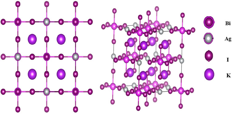
Figure 1 shows the crystal structure of the K2AgBiI6 double perovskites compounds. To ascertain these structural configurations, the unit cells underwent an initial optimization process employing energy minimization, followed by the relaxation of internal parameters. This meticulous exploration was undertaken to delve into the nuances of these architectures. Subsequently, Murnaghan’s equation of state was employed to deduce the lattice constants of the double perovskite structures in their ground state (Del Campo et al., 2012; Al-Hattab et al., 2020). The lattice parameter’s computed value is
The double perovskite compound K2AgBiI6 exhibits a crystalline structure that aligns with cubic symmetry, characterized by the Fm3m (#225) space group. The constituent atoms occupy specific functional coordinates in this arrangement, contributing to the overall crystalline framework. The potassium (K) atoms are positioned at fractional coordinates (0.25, 0.25, 0.75), occupying the 8c Wyckoff site. Similarly, the silver (Ag) atoms are situated at fractional coordinates (0.25, 0, 0), residing within the 4a Wyckoff site. On the other hand, the bismuth (Bi) atoms are coordinated at the origin (0, 0, 0), aligning with the 4b Wyckoff position. Completing this composition, the iodine (I) anions are located at fractional coordinates (0.253643, 0, 0), corresponding to the 24e Wyckoff site.
This arrangement of atoms within the crystal lattice highlights the precise organization and distribution of each element, thereby defining the unique structural properties of the double perovskite K2AgBiI6. Such insight into the positional specifics of these constituent atoms enhances our understanding of the material’s behavior and its potential applications in various scientific and technological domains (Meyer et al., 2018). We have determined the effective masses of electrons in the conduction band and holes in the valence band to analyze these particles’ characteristics. The diagonal elements of influential mass tensor mc are classically dined according to the following formula (2) (Zhao et al., 2018):
The effectiveness of electron
3.2 Material thermodynamic stability
To assess the thermodynamic stability of this double perovskite, we calculated the formation energy of this compound through chemical Equation 3:
The symbol E_tot (K₂AgBiI₆) denotes the comprehensive energy aggregate inherent in the examined halides. Conversely,
The compound K2AgBiI6 exhibits a cubic crystal structure derived from the perovskite arrangement, characterized by its placement within the cubic Fm3m space group. Within this structure, the potassium cations (K1⁺) are intricately linked to twelve identical iodine anions (I1⁻), resulting in the formation of KI₁₂ cuboctahedra. These cuboctahedra are interconnected through shared corners with twelve other equivalent KI₁₂ cuboctahedra, shared faces with six equivalent KI₁₂ cuboctahedra, and further shared faces with four equivalent AgI₆ octahedra as well as four equivalent BiI₆ octahedra. The lengths of all potassium-iodine (K–I) bonds measure 4.30 Å. The silver cations (Ag1⁺) create AgI₆ octahedra in this structure by bonding with six identical iodine anions (I1⁻). These octahedra are characterized by their shared corners with six equivalent BiI₆ octahedra and their shared faces with eight identical KI₁₂ cuboctahedra. Importantly, these octahedra maintain a non-tilted configuration. The distances between silver and iodine (Ag–I) bonds in these octahedra measure 2.99 Å.
Likewise, the bismuth cations (Bi³⁺) form BiI₆ octahedra by bonding with six identical iodine anions (I1⁻). These octahedra share corners with six equivalent AgI₆ octahedra and faces with eight identical KI₁₂ cuboctahedra. Similar to the silver-containing octahedra, these bismuth-based octahedra also maintain a non-tilted orientation. The lengths of bismuth-iodine (Bi–I) bonds in these octahedra measure 3.08 Å. The iodine anions (I1⁻) themselves are linearly bonded to four equivalent potassium cations (K1⁺), one silver cation (Ag1⁺), and one bismuth cation (Bi³⁺). This intricate network of bonding interactions and the precise spatial arrangement of these constituent elements define the unique structural characteristics of K2AgBiI6, shedding light on its potential properties and applications in diverse scientific and technological contexts. Based on databases from materials project (Ali et al., 2023; Jain et al., 2013).
4 Results and discussion
4.1 Electronic propriety
4.1.1 Band structure
Band structure is a critical concept in condensed matter physics and materials science that describes the distribution of energy levels, or bands, in a solid material. It provides information about electrons’ electronic properties and behavior in a crystalline solid. Carried out research on Cs2BiAgBr6 and reported it as an indirect bandgap (Eg = 1.728 eV) compound (Ali et al., 2021). Their experiment and theory also confirmed the indirect band semiconducting nature of Cs2BiAgBr6 along with Cs2BiAgCl6 (Dong et al., 1979). Suggested Rb2AgBiI6 for solar cell applications because of its good optical properties (Mathew et al., 2019), recommend employing Cs2AgInCl6 (Eg = 1.1 eV) for its favorable optoelectronic attributes. In a separate study (Nazir et al., 2023; Madsen and Singh, 2006).
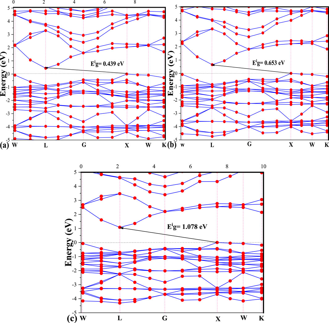
The negative side of energy describes the valence band (VB), while the positive energy side shows the conduction band (CB), separated by the Fermi level Ef. Figure 2 gives us the value of the optical gap of K₂AgBiI₆ in the three approximations; the values of these bandgaps decrease by changing approximation. It has 0.439 eV, 0.653 eV, and 1.078 eV for LDA, GGA, and m-GGA approximations, respectively. The band gap results are similar to this work when it has a value of 0.857 eV using the GGA approximation (Bouich et al., 2022). The band gap of the double perovskite K₂AgBiI₆ is experimentally determined to be approximately 1.95 eV (Chen et al., 2024). This value aligns with similar lead-free perovskites, making it suitable for photovoltaic applications. Other related materials, like Cs₂AgBiBr₆, show slightly higher band gaps around 2.2 eV (Dar et al., 2019). The width of this bandgap is deemed sufficiently small to manifest characteristics akin to those of semiconductors. In the context of the three approximations, we have identified an indirect gap [X, L]. Observably, both the upper and lower regions of the conduction band demonstrate pronounced dispersion in proximity to W, L, and X points. This observation implies substantial mobility, suggesting favorable charge transport properties.
Local Density Approximation (LDA): LDA is the simplest approximation, where the exchange-correlation function is based only on the electron density at each point in the crystal. It assumes that the exchange-correlation energy depends only on the local electron density and is the same for all crystal regions. Although LDA can work well for some materials, it often underestimates the bandgap energy in most cases. Indeed, it neglects some nonlocal correlation effects.
Generalized Gradient Approximation (GGA): GGA is a more sophisticated approximation that considers the electron density and the gradient of the electron density. By accounting for the gradient, GGA can capture some of the nonlocal correlation effects that LDA lacks, improving the accuracy of various properties, including bandgap energy. As a result, GGA tends to provide more considerable bandgap energies than LDA.
Meta-Generalized Gradient Approximation (mGGA): mGGA is even more advanced and accurate than GGA. It includes higher-order derivatives of electron density, allowing it to capture more complex nonlocal correlation effects. The increased accuracy of m-GGA often leads to more considerable bandgap energies than both LDA and GGA (Parrey et al., 2018; Sharma et al., 2016).
The increase in bandgap energy from LDA to GGA to mGGA can be explained by the progressive improvement of the approximations used to describe the exchange-correlation function. As you move from LDA to GGA and then to mGGA, the model becomes more sophisticated and incorporates more accurate descriptions of electronic interactions, resulting in better predictions of bandgap energies. It is important to note that the choice of the exchange-correlation function is crucial in electronic structure calculations, and the most appropriate level of approximation depends on the specific material and properties under study. In some cases, mGGA might be the most accurate choice, while in others, GGA might suffice. It is always good practice to compare the results with experimental data, if available, to validate the chosen approximation and methodology (Saeed et al., 2022; Karouchi et al., 2023).
4.1.2 Density of state
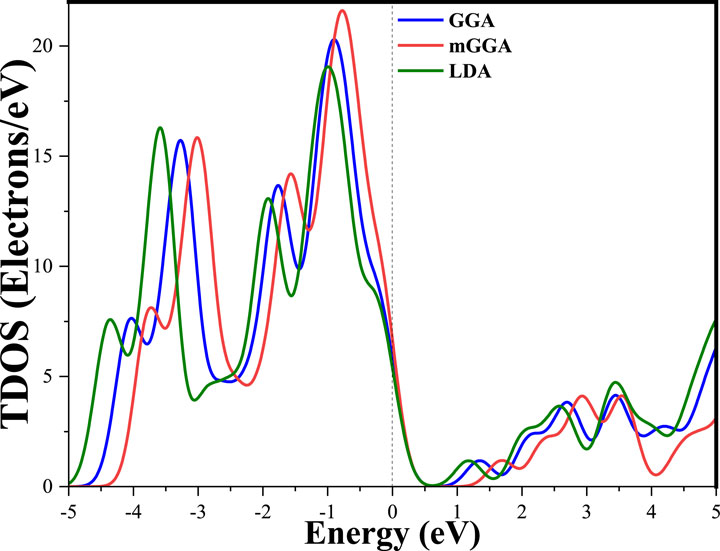
Density of States (DOS) is a fundamental concept in condensed matter physics that provides a statistical description of the distribution of energy states available to electrons in a material. It represents the number of electronic states per unit energy interval at each energy level (Perdew et al., 1996). Figure 3 of the DOS shows that in the valance band, the sharper peaks at around −0.7 eV decreased from 17, 21, and 24 states/eV, respectively, for LDA, GGA, and mGGA approximations. The DOS peaks in the valance region in the energy range increased with the LDA and GGA, compared with the m-GGA method. In the conduction band, every graph of approximation begins in our band gab; these three graphs are, in general, close to each other, with a phase shift equal to the difference between values of the gap.
The plotted Partial Density of States (PDOS) graphs in Figure 4 also provide insight into the electronic contributions. Notably, the p-orbitals associated with the I-atom exhibit significant contributions to the overall Density of States (DOS) within the valence region spanning from −2 to 0. In this range, the contributions from the other atoms are notably marginal. In contrast, within the conduction region, it becomes apparent that the p-states originating from the Bi-atom exert the most substantial influence on the DOS. It is worth mentioning that the DOS peaks, attributable to both the I and Bi atoms, indicate the pronounced presence of halogen and post-transition compounds in this material.
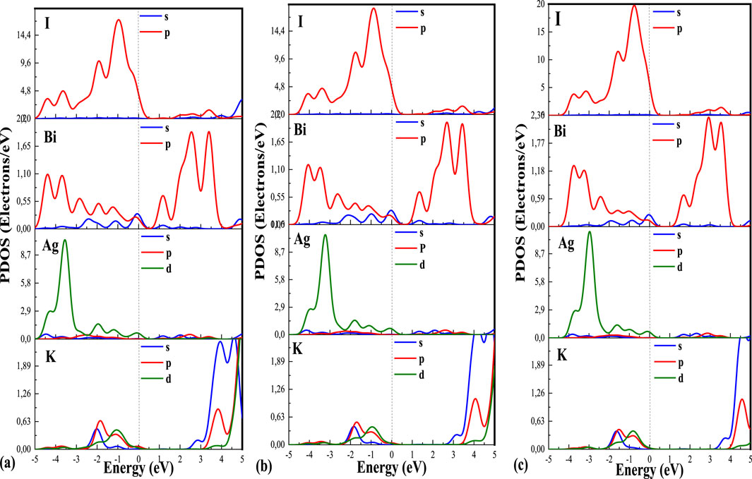
Figure 4. (A–C) are the partial densities of the state of K₂AgBiI₆ by using LDA, GGA, and mGGA, respectively.
Despite the presence of peaks in the DOS, it is essential to note that due to the discernible band gap and the distinct peaks just slightly above the Fermi energy (Ef) (Moulaoui et al., 2023), we draw a preliminary inference that this compound exhibits properties consistent with a semiconducting (Moulaoui et al., 2022a; Moulaoui et al., 2022b). This assessment is based on the approaches of local density approximation (LDA), generalized gradient approximation (GGA), and meta-generalized gradient approximation (m-GGA). The PDOS plots for the K₂AgBiI₆ double perovskite plot the contribution of different atomic orbitals to the electronic density of states (DOS). The x-axis (eV) of the graph corresponds to the energy levels, while the y-axis represents the density of states (Electrons/eV) or intensity of the PDOS. The PDOS is calculated by projecting the electronic states obtained from the DOS calculation onto the localized atomic orbitals of each atom in the K₂AgBiI₆ unit cell. The PDOS plot shows distinct peaks and features that provide valuable insight into the electronic structure and bonding behavior of the K₂AgBiI₆ double perovskite. Each peak is associated with specific atomic orbitals and reflects the contribution of different electron energy levels to the total DOS. Peaks in the valence band region of the PDOS plot correspond to occupied electronic states below the Fermi level. These states represent the electrons present in the valence band of the material. The peaks can be attributed to the contribution of specific atomic orbitals, such as the p and d orbitals of K-site cations, the p and d orbitals of Ag-site cations, the s and p orbitals of Bi-site cations, and the p orbital of I-site anions.
The peaks in the conduction band region of the PDOS plot represent the unoccupied electronic states above the Fermi level (Al-Hattab et al., 2022; Archi et al., 2023). These states are responsible for the material’s electronic conductivity and charge transport properties (Najim et al., 2022; Bajjou et al., 2022). The conduction band peaks are mainly attributed to the contribution of the p orbitals of the Bi-site anions. The intensity and position of these peaks can provide information about the bandgap energy of the material and its suitability for specific electronic applications. The features observed in the PDOS plot provide insight into the bonding and electronic properties of the K₂AgBiI₆ double perovskite. The PDOS plot can also reveal the presence of impurity states or defect levels that influence material properties. By describing the peaks and curves of the PDOS plot of the double perovskite K₂AgBiI₆ using this approach, researchers can gain a comprehensive understanding of its electronic structure, bonding behavior, and potential applications in various fields of materials science.
5 Optical proprieties
5.1 Dielectric function, absorption and reflectivity
When investigating a material’s optical characteristics, it is critical to calculate and interpret the complicated dielectric function. The function is essential since it allows us to calculate the other optical qualities. Its optical characteristics. Furthermore, the imaginary portion,
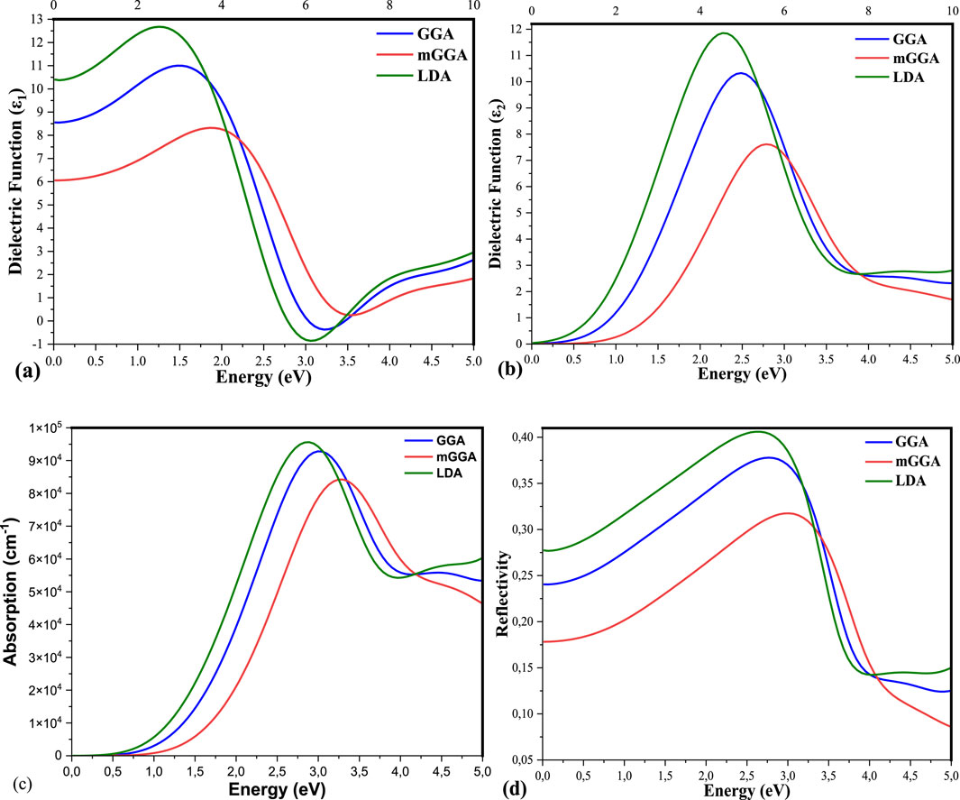
Figure 5. (A–D) are the Real, Imaginary dielectric function, Absorption, and Reflectivity of the state of K₂AgBiI₆ by using LDA, GGA, and mGGA respectively.
5.2 Optical conductivity
Electron conduction is due to an applied electromagnetic field characterized by optical conductivity (Nazir et al., 2023; Ejjabli et al., 2024). Figures 6A, B shows that the real and imaginary optical conductivity

Figure 6. (A, B) are Real and Imaginary Conductivity of the state of K₂AgBiI₆ by using LDA, GGA, and mGGA, respectively.
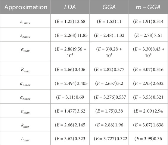
Table 1. Maximum values calculated for
5.3 Refractive index, extinction coefficient, and loss function
Knowledge of the refractive index dispersion
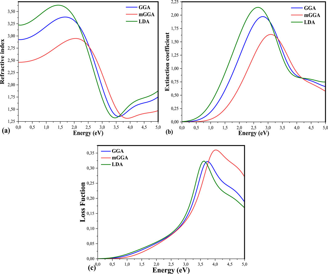
Figure 7. (A–C) are the Refractive Index, Extinction Coefficient, and Loss Function of the state of K₂AgBiI₆ by using LDA, GGA, and mGGA, respectively.
Maximum refractive index values and extinction coefficients for
6 Conclusion
In this study, we delved into the intricate electronic properties of the perovskite material using a comprehensive approach by employing three distinct approximations: LDA, GGA, and mGGA. Our investigation aimed to unravel the multifaceted interplay between theoretical models and the electronic behavior of the perovskite structure. Through rigorous computations, we uncovered compelling insights into the nature of the electronic structure within the perovskite framework. We find indirect band gap egal 0.439 eV, 0.653 eV, and 1.078 eV for LDA, GGA, and mGGA approximations, respectively. With its simplicity and computational efficiency, the LDA approximation offered a valuable initial glimpse into the material’s properties. The GGA approach refined our understanding by incorporating gradient corrections, accurately capturing electronic interactions, and shedding light on crucial bandgap characteristics. However, the most captivating revelations emerged from the mGGA approximation. By considering meta-generalized gradient corrections, we witnessed a remarkable convergence between theoretical predictions and experimental observations. This advanced approach discerned intricate electronic nuances and revealed the material’s sensitivity to subtle electronic rearrangements. Our findings underscore the importance of methodological choices in modeling perovskite materials, with each approximation offering a distinct lens through which to perceive their electronic intricacies. As the pursuit of efficient and high-performance photovoltaic materials intensifies, our study serves as a testament to the significance of comprehensive theoretical investigations in guiding the design and optimization of materials for cutting-edge applications.
Data availability statement
The original contributions presented in the study are included in the article/Supplementary Material, further inquiries can be directed to the corresponding author.
Author contributions
MK: Conceptualization, Data curation, Formal Analysis, Investigation, Methodology, Writing–original draft. AE: Conceptualization, Formal Analysis, Investigation, Validation, Visualization, Writing–review and editing. OB: Investigation, Methodology, Resources, Writing–original draft. JG: Data curation, Investigation, Methodology, Visualization, Writing–review and editing. MA-H: Investigation, Methodology, Resources, Validation, Writing–review and editing. MB-MK: Formal Analysis, Investigation, Validation, Visualization, Writing–review and editing. KR: Funding acquisition, Investigation, Methodology, Resources, Software, Writing–review and editing. YL: Investigation, Methodology, Project administration, Supervision, Validation, Writing–review and editing.
Funding
The author(s) declare that no financial support was received for the research, authorship, and/or publication of this article.
Acknowledgments
The authors sincerely thank all who contributed to this scientific work, notably Sultan Moulay Slimane University and UNISA University.
Conflict of interest
The authors declare that the research was conducted in the absence of any commercial or financial relationships that could be construed as a potential conflict of interest.
Publisher’s note
All claims expressed in this article are solely those of the authors and do not necessarily represent those of their affiliated organizations, or those of the publisher, the editors and the reviewers. Any product that may be evaluated in this article, or claim that may be made by its manufacturer, is not guaranteed or endorsed by the publisher.
References
Al-Hattab, M., Moudou, L., Chrafih, Y., Khenfouch, M., Bajjou, O., and Rahmani, K. (2020). The anisotropic optical properties of different polytypes (ε,β,δ,γ) of GaSe lamellar materials. EPJ Appl. Phys. 91 (3), 30102. doi:10.1051/epjap/2020200136
Al-Hattab, M., Moudou, L., Chrafih, younes, Rahmani, K., Khenfouch, M., and Bajjou, O. (2022). First-principles calculation of the structural, electronic and optical properties of GaSe_(1-x) S_(x) (x = 0, 0.25, 0.5 and 1) compounds. Adv. Mater. Process. Technol. 8 (3), 2731–2743. doi:10.1080/2374068X.2021.1939991
Ali, M. A., Alshahrani, T., and Murtaza, G. (2021). Defective perovskites Cs2SeCl6 and Cs2TeCl6 as novel high temperature potential thermoelectric materials. Mater Sci. Semicond. Process 127 (Jun), 105728. doi:10.1016/j.mssp.2021.105728
Ali, M. A., Alshgari, R. A., Awadh Bahajjaj, A. A., and Sillanpää, M. (2023). The study of new double perovskites K2AgAsX6 (X = Cl, Br) for energy-based applications. J. Taibah Univ. Sci. 17 (1). doi:10.1080/16583655.2023.2170680
Archi, M., Bajjou, O., Moulaoui, L., Najim, A., Karouchi, M., Rahmani, K., et al. (2023). Electronic and optical properties of different concentrations of Ga doped ZnO: CASTEP study. IEEE. doi:10.1109/IRASET57153.2023.10152942
Bajjou, O., Najim, A., Rahmani, K., and Khenfouch, M. (2022). First-principles study on electronic and optical properties of single-walled carbon nanotube under an external electric field. J. Mol. Model. 28 (4), 97. doi:10.1007/s00894-022-05090-2
Benmhidi, H., Rached, H., Rached, D., and Benkabou, M. (2017). Ab initio study of electronic structure, elastic and transport properties of fluoroperovskite LiBeF3. J. Electron Mater 46 (4), 2205–2210. doi:10.1007/s11664-016-5159-0
Bhorde, A., Waykar, R., Rondiya, S. R., Nair, S., Lonkar, G., Funde, A., et al. (2021). Structural, electronic, and optical properties of lead-free halide double perovskite Rb2AgBiI6: a combined experimental and density functional theory study. ES Mater. Manuf. 12, 43–52. doi:10.30919/esmm5f1042
Bouich, A. (2020). Study and characterization of hybrid perovskites and copper-indium-gallium selenide thin films for tandem solar cells. Universitat Politècnica de València. https://riunet.upv.es/bitstream/id/868827/Bouich%20-%20Study%20and%20Characterization%20of%20Hybrid%20Perovskites%20and%20Copper-Indium-Gallium%20Selenide%20thin.pdf
Bouich, A., Marí-Guaita, J., Sahraoui, B., Palacios, P., and Marí, B. (2022). Tetrabutylammonium (TBA)-Doped methylammonium lead iodide: high quality and stable perovskite thin films. Front. Energy Res. 10. doi:10.3389/fenrg.2022.840817
Bourachid, I., Caid, M., Cheref, O., Rached, D., Heireche, H., Abidri, B., et al. (2020). Insight into the structural, electronic, mechanical and optical properties of inorganic lead bromide perovskite APbBr3 (A = Li, Na, K, Rb, and Cs). Comput. Condens. Matter 24 (Sep), e00478. doi:10.1016/j.cocom.2020.e00478
Chen, Q., Zhou, L., Zhang, J., Chen, D., Zhu, W., Xi, H., et al. (2024). Recent progress of wide bandgap perovskites towards two-terminal perovskite/silicon tandem solar cells. Nanomaterials 14 (2), 202. doi:10.3390/nano14020202
Cs, P., Filip, M. R., Hillman, S., Abbas Haghighirad, A., Snaith, H. J., and Giustino, F. (2016). Band gaps of the lead-free halide double from theory and experiment.
Dar, S. A., Ali, M. A., and Srivastava, V. (2020). Investigation on bismuth-based oxide perovskites MBiO3 (M = Rb, Cs, Tl) for structural, electronic, mechanical and thermal properties. Eur. Phys. J. B 93 (6), 102. doi:10.1140/epjb/e2020-10073-x
Dar, S. A., Sharma, R., Srivastava, V., and Sakalle, U. K. (2019). Investigation on the electronic structure, optical, elastic, mechanical, thermodynamic and thermoelectric properties of wide band gap semiconductor double perovskite Ba 2 InTaO 6. RSC Adv. 9 (17), 9522–9532. doi:10.1039/C9RA00313D
Del Campo, J. M., Gázquez, J. L., Trickey, S. B., and Vela, A. (2012). Non-empirical improvement of PBE and its hybrid PBE0 for general description of molecular properties. J. Chem. Phys. 136 (10), 104108. doi:10.1063/1.3691197
Dong, Q., Fang, Y., Shao, Y., Mulligan, P., Qiu, J., Cao, L., et al. (1979). Electron-hole diffusion lengths > 175 μm in solution-grown CH3NH3PbI3 single crystals,” Science. 347, no. 6225, pp. 967–970. doi:10.1126/science.aaa5760
Ejjabli, A., Karouchi, M., Al-Hattab, M., Bajjou, O., Rahmani, K., and Lachtioui, Y. (2024). Investigation of lead-free halide K2AgSbBr6 double Perovskite’s structural, electronic, and optical properties using DFT functionals. Chem. Phys. Impact 9, 100656. doi:10.1016/j.chphi.2024.100656
Jain, A., Ong, S. P., Hautier, G., Chen, W., Richards, W. D., Dacek, S., et al. (2013). Commentary: the materials project: a materials genome approach to accelerating materials innovation. Apl. Mater. 1 (1). doi:10.1063/1.4812323
Karouchi, M., Marouane, A., Bajjou, O., Moulaoui, L., Najim, A., Rahmani, K., et al. (2023). “Increasing electro-optical properties of perovskite FAPbI3 under the effect of doping by Sn,” in 2023 3rd international conference on innovative research in applied science, engineering and technology (IRASET) (IEEE), 1–7. doi:10.1109/IRASET57153.2023.10152963
Lozhkina, O. A., Murashkina, A., Elizarov, M., Shilovskikh, V., Zolotarev, A., Kapitonov, Y. V., et al. (2018). Microstructural analysis and optical properties of the halide double perovskite Cs2BiAgBr6 single crystals. Chem. Phys. Lett. 694, 18–22. doi:10.1016/j.cplett.2018.01.031
Madsen, G. K. H., and Singh, D. J. (2006). BoltzTraP. A code for calculating band-structure dependent quantities. Comput. Phys. Commun. 175 (1), 67–71. doi:10.1016/j.cpc.2006.03.007
Mathew, N. P., Kumar, N. R., and Radhakrishnan, R. (2019). “First principle study of the structural and optoelectronic properties of direct bandgap double perovskite Cs2AgInCl6,” in Materials today: proceedings (Elsevier Ltd), 1252–1256. doi:10.1016/j.matpr.2020.03.489
Meyer, E., Mutukwa, D., Zingwe, N., and Taziwa, R. (2018). Lead-free halide double perovskites: a review of the structural, optical, and stability properties as well as their viability to replace lead halide perovskites. Metals 8, 667. doi:10.3390/met8090667
Mir, S. A., and Gupta, D. C. (2021). Structural and mechanical stabilities, electronic, magnetic and thermophysical properties of double perovskite 2: probed by DFT computation. Int. J. Energy Res. 45 (10), 14603–14611. doi:10.1002/er.6720
Moulaoui, L., Bajjou, O., Lachtioui, Y., Najim, A., Archi, M., Rahmani, K., et al. (2023). Modeling of highly efficient lead-free MASnI3-based solar cell with graphene oxide as hole transport layer using SCAPS-1D. J. Electron. Mater. 52, 7541–7553. doi:10.1007/s11664-023-10684-4
Moulaoui, L., Bajjou, O., Najim, A., Archi, M., and Rahmani, K. (2022a). Numerical simulation of the NiO as hole transport layer in CH3NH3PbBr3perovskite based-solar cell using SCAPS-1D. IEEE. doi:10.1109/IRASET52964.2022.9737984
Moulaoui, L., Bajjou, O., Najim, A., and Rahmani, K. (2022b). The study of electronic and optical properties of perovskites CH3NH3PbCl3and CH3NH3PbBr3using first-principle. E3S Web Conf. 336, 00015. doi:10.1051/e3sconf/202233600015
Moulaoui, L., Bajjou, O., Najim, A., Rahmani, K., Archi, M., Laassouli, A., et al. (2023). Numerical Simulation of FAPbI3perovskite based solar cells with graphene oxide as hole transport layer using SCAPS-1D. IEEE. doi:10.1109/IRASET57153.2023.10153032
Najim, A., Bajjou, O., Boulghallat, M., Khenfouch, M., Rahmani, K., and Chrafih, Y. (2022). First-principles calculations to investigate the influence of porphyrin substitution on the structural, electronic and optical properties of graphene oxide. J. Optik 257, 168874. doi:10.1016/j.ijleo.2022.168874
Nazir, G., Mahmood, Q., Hassan, M., AL-Anazy, M. M., Kattan, N. A., Sfina, N., et al. (2023). Tuning of band gap by anions (Cl, Br, I) of double perovskites Rb 2 AgAsX 6 (Cl, Br, I) for solar cells and thermoelectric applications. Phys. Scr 98 (2), 025811. doi:10.1088/1402-4896/acaec1
Parrey, K. A., Khandy, S. A., Islam, I., Laref, A., Gupta, D. C., Niazi, A., et al. (2018). Correction to: electronic structure, optical and transport properties of double perovskite La2NbMnO6: a theoretical understanding from DFT calculations. J. Electron. Mater. 47 (7), 4209. doi:10.1007/s11664-018-6361-z
Saeed, M., Haq, I. U., Saleemi, A. S., Rehman, S. U., Haq, B. U., Chaudhry, A. R., et al. (2022). First-principles prediction of the ground-state crystal structure of double-perovskite halides Cs2AgCrX6 (X = Cl, Br, and I). J. Phys. Chem. Solids 160, 110302. doi:10.1016/j.jpcs.2021.110302
Sharma, S., Sharma, J., and Sharma, Y. (2016). DFT calculations of electronic and optical properties of SrS with LDA. GGA and mGGA functionals, 020095. doi:10.1063/1.4946146
Wang, L., Yao, P., Wang, F., Li, S., Chen, Y., Xia, T., et al. (2020). Pressure-induced structural evolution and bandgap optimization of lead-free halide double perovskite (NH4)2SeBr6. Adv. Sci. 7 (6), 1902900. doi:10.1002/advs.201902900
Keywords: double perovskite (K2AgBiI6), solar cell, electronic properties, optical properties, structural properties, DFT
Citation: Karouchi M, Ejjabli A, Bajjou O, Guerroum J, Al-Hattab M, Basyooni-M. Kabatas MA, Rahmani K and Lachtioui Y (2024) Investigating the structural, electronic, and optical properties of the novel double perovskite K2AgBiI6 using DFT. Front. Mater. 11:1448400. doi: 10.3389/fmats.2024.1448400
Received: 13 June 2024; Accepted: 21 August 2024;
Published: 03 September 2024.
Edited by:
İlknur Erucar, Özyeğin University, TürkiyeReviewed by:
Amal Bouich, Universitat Politècnica de València, SpainTarek Hidouri, University of Parma, Italy
Copyright © 2024 Karouchi, Ejjabli, Bajjou, Guerroum, Al-Hattab, Basyooni-M. Kabatas, Rahmani and Lachtioui. This is an open-access article distributed under the terms of the Creative Commons Attribution License (CC BY). The use, distribution or reproduction in other forums is permitted, provided the original author(s) and the copyright owner(s) are credited and that the original publication in this journal is cited, in accordance with accepted academic practice. No use, distribution or reproduction is permitted which does not comply with these terms.
*Correspondence: Mohamed A. Basyooni-M. Kabatas, bS5hLmJhc3lvb25pQGdtYWlsLmNvbQ==, bS5rYWJhdGFzQHR1ZGVsZnQubmw=
 Mohamed Karouchi
 Abdelkebir Ejjabli
 Omar Bajjou
 Jamal Guerroum1
 Mohamed Al-Hattab
 Mohamed A. Basyooni-M. Kabatas