
95% of researchers rate our articles as excellent or good
Learn more about the work of our research integrity team to safeguard the quality of each article we publish.
Find out more
ORIGINAL RESEARCH article
Front. Mater. , 12 January 2024
Sec. Thin Solid Films
Volume 10 - 2023 | https://doi.org/10.3389/fmats.2023.1337925
 Abdulilah Mohammad Mayet1*Mohammed Abdul Muqeet1Hala H. Alhashim2Fadi Kurdahi3
 Ehsan Eftekhari-Zadeh4*
Introduction: The mechanical nature of nanoelectromechanical (NEM) switches makes them sluggish yet desirable for ultra-low-power, harsh environment applications. Two- and three-terminal NEM switches have been demonstrated using onedimensional, two-dimensional, and thin films, but sub-0.3 V operation with improved mechanical and electrical reliability is still elusive.
Method: This study presents WNxnano-ribbon-based NEM sensor switches that operate at 0.6 V, 30 nanosecond switching time, 8 trillion cycles, and 0.5 mA ON current with less than 5 kΩ ON resistance, without stiction, mechanical welding, or short circuits. WNx’s high Young’s modulus gives it great elasticity and mechanical restoring force, which may overcome van der Waal and capillary forces.
Results and Discussion: With its high Young’s modulus, the device’s nanoscale size facilitated low operating voltage. WNxnano-ribbon without grain boundaries is amorphous and more mechanically strong. Hammering and high current flow may destroy the nano-ribbon contact surface and interface, which is practically immaculate. Pull-out time (dominant delay factor) is 0 owing to high Young’s modulus, hence hysteresis loss and delay are absent. Elasticity and Young’s modulus increase speed.
Nanotechnology, an interdisciplinary field encompassing the investigation, creation, and implementation of systems characterized by their nanometer-scale dimensions or tolerances, is increasingly assuming a position of significance across diverse domains. The impetus behind the advancement of nanotechnologies and nanoscience stems from a diverse array of industries and applications. Concurrently, this progress propels the exploration of forthcoming industrial and practical applications within the field itself. The attainment of manufacturing processes at the sub-nanometer level of precision, which is imperative for the realization of essential features and accurate positioning activities, stands as a paramount concern within the realm of contemporary nanotechnology. According to Moore’s law, it is postulated that the ongoing reduction in chip sizes will facilitate the integration of increasingly intricate systems endowed with heightened portability and intelligence within forthcoming technological advancements. Hence, it can be inferred that a multifunctional machine will possess a compact configuration. According to scholarly discourse, it has been posited by experts that MEMS, or Microelectromechanical Systems, can be aptly characterized as embodying the “More than Moore” paradigm (Fang et al., 2013; Loh and Espinosa, 2012). The conceptualization of employing Silicon (Si) as a medium for the fabrication of Microelectromechanical Systems (MEMS) and Nanoelectromechanical Systems (NEMS) devices emerged from the recognition that integrating MEMS structures with the extensively advanced Si-based electronic circuitry and devices on a shared Si substrate could yield compact, dependable, and energy-efficient Si-based MEMS/NEMS devices (Auciello and Aslam, 2021). On the contrary, it is worth noting that silicon (Si) exhibits certain constraints in terms of its mechanical and surface tensile properties, which are of utmost significance when considering the functionality and performance of microelectromechanical systems (MEMS) devices. In comparison to numerous other materials, it is noteworthy that silicon exhibits a relatively inferior Young’s modulus and fracture toughness, alongside a significant coefficient of friction (COF) and propensity for abrasive wear. These characteristics collectively contribute to the considerable energy dissipation observed in silicon-based microelectromechanical systems (MEMS) devices, primarily attributable to the frictional forces exerted by their mobile components. In addition, it is worth noting that silicon-based microelectromechanical systems (MEMS) devices incorporating mobile components that exhibit rapid rolling or sliding motion are prone to mechanical degradation, ultimately leading to failure (Lu et al., 2018; Shen et al., 2021). The miniaturization of RF systems is a topic of considerable interest, and within this domain, the RF MEMS switch has garnered significant attention as a highly advantageous constituent. The utilization of Tunnel Field-Effect Transistors (TFETs) in Radio Frequency (RF) systems has become obsolete primarily due to their suboptimal operational characteristics at RF frequencies, as well as their substantial power consumption, notable insertion and return loss, insufficient isolation, and unwieldy physical construction. As a result, RF MEMS switches have assumed their designated position (Saleem and Nawaz, 2019; Shukla et al., 2022).
A micro-electromechanical systems (MEMS) switch, which exhibits notable switching speeds, has been successfully devised through the utilization of a micro-cantilever structure. Cantilevers, in their fundamental configuration, constitute an integral component of any mechanical system that affords unrestricted mobility in either the vertical or horizontal plane at one extremity. The utilization of cantilevers in the development of radio frequency microelectromechanical systems (RF MEMS) switches presents both advantages and disadvantages. The utilization of cantilever-based microelectromechanical systems (MEMS) switches in radio-frequency (RF) circuits and devices is constrained due to challenges associated with stiction and reliability arising from the metal-to-metal contact established in their “bending” configuration. Prior studies have demonstrated that cantilever switches exhibit superior performance in terms of both switching time and release when compared to capacitive switches (Kurmendra and Kumar, 2021a; Kurmendra and Kumar, 2021b; Kumari and Angira, 2022; Kurmendra and Kumar, 2022; XJ He et al., 2012; Koul and Dey, 2022; Riverola et al., 2016a). The efficacy of a coiled micro-cantilever switch, which exhibits a thermally responsive behavior, was investigated by a team of researchers. The temporal duration of a switch’s release is observed to exhibit an elongation ranging from 5% to 13% when compared to switches based on planar cantilever configurations. The utilization of RF MEMS switches has been identified across various disciplines (Nakajima et al., 2017; Shen et al., 2021; Kurmendra and Kumar, 2021a; Riverola et al., 2016a; Hähnlein et al., 2017). Casimir’s force increases as the square root of the inverse of the square of the gap (Koul and Dey, 2022; Duan and Rach, 2013; Tsai and Li, 2022). The boundary value problem (BVP) involving the nano-beam deflection model with dispersed parameters presents a significant challenge in obtaining an analytical solution due to the utilization of Ashby’s methodology for the nonlinear governing equation (Lu et al., 2018; Kurmendra and Kumar, 2021b; Kurmendra and Kumar, 2022; Duan and Rach, 2013; Tian et al., 2016). Certain researchers have undertaken a study on the dynamic behavior of nano-scale electrostatic actuators, with a particular focus on incorporating the influence of the van der Waals force. The objective of this investigation is to develop approximate analytic solutions to address this matter (Saleem and Nawaz, 2019; Duan and Rach, 2013; Tsai and Li, 2022).
In contrast to contemporary state-of-the-art technologies, the authors assert the existence of four noteworthy potential innovations, namely, Ultra-Low Voltage Operation, Unprecedented Cycle Longevity, Amorphous Metal as a Structural Material, and the Potential for Nanoscale Integration. The employment of amorphous metal WNx, within the realm of nanoelectromechanical systems (NEMS) switches facilitates their operation at remarkably diminished voltage levels, notably below the threshold of 0.3 V. The aforementioned accomplishment is of considerable significance due to its implication of diminished power consumption and enhanced energy efficiency. This holds paramount importance for the progression of low-power electronics and the Internet of Things (IoT). The assertion pertaining to the magnitude of 8 trillion cycles posits an extraordinary level of endurance and dependability exhibited by the NEMS switch. The attainment of a considerable magnitude of cycles holds substantial implications, as it has the potential to effectively mitigate apprehensions pertaining to the durability of nano-fabricated switches. The aforementioned observations possess the potential to yield significant ramifications for various applications that necessitate sustained and resilient functionality, such as those pertaining to memory storage or computational components. The selection of an amorphous metal as the structural material for the switch is of considerable significance. The absence of a crystalline structure, which is characteristic of conventional metals, confers several notable benefits, including heightened hardness, superior resistance to wear, and enhanced electrical conductivity. The incorporation of amorphous metal within NEMS switches presents a promising opportunity to explore novel pathways for the development of nanoscale devices that exhibit exceptional performance and longevity. The utilization of nanoelectromechanical systems (NEMS) entails the operation of switches at the nanoscale. The significance of this cannot be overstated in light of the prevailing trajectory towards the diminution of scale in the realm of electronic devices. The reliable control and manipulation of nanoscale components are imperative for the advancement of sophisticated computing architectures, sensors, and communication devices. The enumerated attributes of the aforementioned NEMS switch render it a viable contender for a multitude of nascent technologies, including but not limited to neuromorphic computing, wherein the indispensability of components exhibiting low power consumption and exceptional dependability is paramount. Furthermore, this technology exhibits potential for utilization in sophisticated memory devices, nanoscale sensing apparatus, and various other domains that necessitate the presence of efficient and long-lasting switches.
In order to fully realize the optimal performance and reliability capabilities of NEM switches, it is imperative to address several underlying challenges. These challenges include the necessity for a lower pull-in voltage (Vpi) that is on par with the current advancements in complementary metal-oxide-semiconductor (CMOS) technology. Additionally, the operability of NEM switches in ambient or air conditions must be enhanced. Furthermore, there is a need for improved ON current and reduced ON resistance in these switches. Moreover, achieving device scalability is a crucial aspect that needs to be considered. Additionally, the mechanical and electrical connections of NEM switches should be upgraded to ensure their efficacy. Lastly, it is essential to augment the endurance of these switches. The subsequent section of this article endeavors to effectively elucidate the process of overcoming and addressing the aforementioned challenges through the utilization of amorphous metal tungsten nitride (αWNx) nano-ribbon, thereby leading to the attainment of an optimal design.
NEM switches can be characterized as mechanical switches that incorporate an active component, typically a movable cantilever that is unilaterally or bilaterally clamped. As seen in Figure 1A, the cantilever is propelled forward by an electrostatic force denoted by the symbol “Fe,” which is generated by the opposing fixed and stiff electrode. The conceptualization of the dynamic and static components can be likened to the metaphorical representation of two capacitor plates. The inherent mechanical restoring force (Fm) of the active component serves to counterbalance the electrostatic force exerted by the surrounding environment (Fe). The operational dynamics of NEM switches encompass a confluence of mechanical and electrical processes that transpire concurrently. Acceleration, deceleration, impact in a hammered form, damping, and resonance are all illustrative instances of mechanical phenomena. Electric charge, dissipation, heightened electrical flow, accumulation of charge, and expeditious discharge are instances of electrical phenomena. The operational intricacy of NEM switches necessitates the active element and electrode material to undergo rapid deterioration, thereby leading to a diminished switch lifespan and compromised electrical performance. The various complications associated with NEM switches can be categorized into four distinct groups: (i) instances of contact area impairment resulting from electrical discharge, (ii) electrode erosion and degradation, (iii) disturbances in functionality, and (iv) mechanical imperfections such as fractures and fatigue within the active segment, as visually depicted in Figures 1B–G.
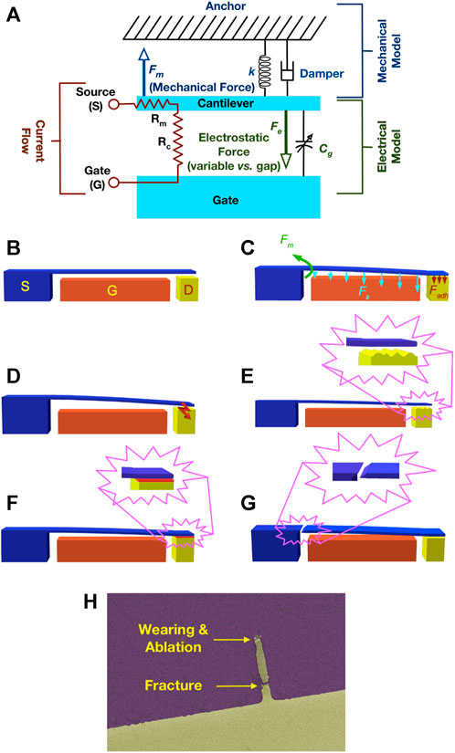
FIGURE 1. Nano-Electro-Mechanical switch; (A) electromagnetic analogous wiring and design in various circumstances; (B) inactive status; (C) drove in status; (D) electric discharge fault; (E) ablation fault; (F) stiction fault; (G) rupture fault; (H) a scanning electron microscope (SEM) image depicting a defective NEM switch subsequent to enduring a multitude of cycles shall be presented for comprehensive analysis.
Figure 1B depicts the top view of an idle state of a vertically actuated three-terminal NEM (Nanoelectromechanical) switch. The operational modality is depicted in Figure 1C wherein the active element establishes contact with the electrode. The relocation of the active component in proximity to the electrode engenders the emergence of a voltage disparity, which exhibits a direct proportionality to the spatial separation between the two entities. Figure 1 depicts the potential occurrence of an electric discharge (commonly referred to as a spark) (d) resulting from the accumulation of charges on a highly irregular surface. The occurrence of a material meltdown is a plausible outcome resulting from an electrical discharge, commonly referred to as burn-out. As can be seen in Figure 1E, an electric discharge may cause ablation and damage to the electrode surface. At the site of contact, the active element undergoes a state of equilibrium wherein it is subject to various forces, most notably the electrostatic force (Fe). The aforementioned forces are frequently attributed to the influence of the pull-in voltage. In addition to the van der Waals and Casimir forces, that collectively exert a pull on the element in the direction of the electrode. Additionally, the mechanical restoring force (Fm) operates externally to the electrode. The state of equilibrium is attained when the aforementioned forces are harmoniously balanced.
As seen in Figure 1F, stiction occurs when the active element is not replaced in its original position when the Fe is no longer present. Elevated spring constant (high Young’s modulus) should be used in order to solve the stiction problem. Amorphous tungsten nitride exhibits advantageous tribological characteristics pertaining to friction and wear. The selection of materials possessing augmented tribological properties serves to mitigate stiction, an undesirable phenomenon characterized by the adhesion between mobile components within a nanoelectromechanical (NEM) switch. The attainment of reduced stiction is of the utmost significance in ensuring the dependable and optimal functioning of a system. The inherent lack of crystalline structure in tungsten nitride films can potentially yield a more refined and polished surface texture. The implementation of smooth surfaces has the potential to effectively mitigate friction and adhesion forces, thereby diminishing the probability of encountering stiction-related complications. Tungsten nitride is renowned for its exceptional electrical conductivity. In the context of the NEM switch, the utilization of a conductive layer can effectively facilitate the transfer of charges, thereby offering the potential for reduced voltage prerequisites for actuation. Tungsten nitride films have been observed to possess favorable dielectric properties. The optimization of these properties has the potential to yield a reduction in energy consumption during the switching process, thereby potentially mitigating voltage requirements.
High Young’s modulus, on the other hand, causes a high pull-in voltage since the two are intimately related. The NEMS switch should be manufactured with reduced size to address this problem (gap and thickness). Finally, the moving portion will fail mechanically if the NEM switch continues to work normally without encountering any of the problems listed above. Material fatigue and fracture near the anchor are terms used to describe this failure as shown in Figure 1G (Loh and Espinosa, 2012). The grain boundary inter-stress and flaws are to blame for this failure. The material’s strength and electrical and thermal conductivity suffer as a result of these flaws. Because of this failure, NEM switches have a short lifespan of only a few million cycles. Due to wear and fracture, the cantilever in Figure 1H is deficient with the utilization of gold (Au).
In order to effectively address the aforementioned concerns, this article centers its attention on the utilization of a structural material that possesses a state of perfect amorphousness, thereby allowing for dimensional scalability. Moreover, it is noteworthy to mention that this particular material possesses two prominent attributes, namely, an exceptionally minimal exterior imperfections and an effectively balanced Young’s modulus. The latter property is of particular importance as it serves as a suitable counterforce against stiction, while simultaneously minimizing the potential risks associated with higher pull-in voltage. This advantageous trade-off is further bolstered by the implementation of dimensional scaling. Amorphous materials possess the advantageous characteristic of being amenable to scalability down to the nanoscale, while concurrently exhibiting a notable absence of structural flaws. Concurrently, it is observed that materials possessing a high Young’s modulus exhibit enhanced rigidity, thereby leading to an augmented switching frequency, consequently yielding improved switching speed. Thus far, a variety of materials encompassing both mono and poly-crystalline compositions have been subjected to investigation in order to tackle these challenges. However, it is worth noting that a definitive breakthrough solution has yet to manifest itself as a pioneering frontrunner (Feng et al., 2015; Chong et al., 2012; Alqahtani et al., 2022).
Consequently, the present article has elected to designate the amorphous WNxnano-ribbon as an exceptional material for employment in NEM switches and conceivably, NEM systems. Despite the fact that polycrystallinity introduces irregularities in the construction of nano-scale devices, the primary focus of this article is exclusively centered on the utilization of amorphous metals. A comprehensive investigation employing the finite element method was conducted to examine the impact of varying crystalline sizes, specifically within the range of 50–90 nm, on the pull-in voltage of polycrystalline tungsten nitride. The results of this study revealed a discernible variance in the pull-in voltage, which ranged from 3.1 to 2.6 V. The observed variability in the pull-in voltage can be primarily attributed to the elevated edge roughness inherent in the polycrystalline structure. This phenomenon can be quantified by expressing the pull-in voltage (Vpi) as a function of the crystalline size (C), yielding the equation Vpi = 3.7–0.13C. The observed alteration in the pull-in voltage exhibits a level of similarity to the variability observed in the threshold voltage of transistors, thereby rendering both phenomena undesirable.
The material known as WNx exhibits an atomic framework devoid of grains, rendering it impervious to rusting. Furthermore, it possesses exceptional longevity, boasting a remarkably uniform exterior. Additionally, this material demonstrates commendable opposition to wear and aggravation (Gu et al., 2014). This is of utmost importance to recognize the inherent disparities that manifest among the categories of non-crystalline metallic material. A process of continuous cooling, commencing from the liquid state, engenders the production of metallic glass, an exceptional metallic variant distinguished by its amorphous atomic arrangement. The term “amorphous metal” is utilized to describe metallic materials that lack a crystalline structure and are produced through methods such as chemical vapor deposition (CVD) or physical vapor deposition (PVD), rather than liquid deposition. The present investigation employs a reactive sputtering methodology utilizing a physical vapor deposition (PVD) instrument, specifically the NEXDEP 200 manufactured by Angstrom Engineering, in conjunction with a tungsten (W) target. The primary objective is to fabricate amorphous tungsten nitride (WNx) films. In light of the numerous alternatives available for the selection of an amorphous material, the authors have made the deliberate choice to opt for a tungsten (W) based nitride alloy, motivated by the subsequent rationales: The first noteworthy aspect pertains to the intrinsic material characteristic of tungsten. Tungsten, being classified as a transition metal, possesses a straightforward crystalline structure. This characteristic extends to its nitride counterpart as well. Notably, these crystalline structures can be conveniently altered to assume amorphous film configurations. Moving on, the second aspect of significance revolves around the commercial availability of tungsten. This factor plays a pivotal role in the feasibility and practicality of utilizing tungsten in various applications. The third aspect deserving attention is the economic aspect. Considering the cost implications associated with material selection, tungsten emerges as a favorable choice due to its favorable economic attributes. Lastly, the compatibility of tungsten with complementary metal-oxide-semiconductor (CMOS) technology warrants consideration.
Unlike the majority of other metals, tungsten exhibits a unique property that allows for its facile micro-machining through the utilization of a conventional reactive ion etching (RIE) technique. This technique involves the use of either SF6 or Cl2 gases, further enhancing the compatibility of tungsten with CMOS processes. The aforementioned characteristic serves as a discriminant between W and silicon carbide (SiC) or hard metals necessitating focus ion beam (FIB) micromachining. Moreover, it is worth noting that tungsten, classified as a transition metal, exhibits a notable density of approximately 19.3 g per cubic centimeter and possesses a remarkably high melting point of 3,410°C. Distinct molecular structures can be observed in crystalline, polycrystalline, and amorphous WNx, as depicted in Supplementary Figure S1. Amorphous WNx has a very high melting point, toughness, and electrical conductivity. Chemical stability is ensured by the guided metal-nonmetal hybrid bonding present in the molecule. For the purpose of fabricating amorphous WNx, this has been proposed by a number of researchers. Crystallization starts at high temperatures, as demonstrated in Figure 2A, hence the amorphous WNx found was not really amorphous (Addonizio et al., 2012; Chen et al., 2012).
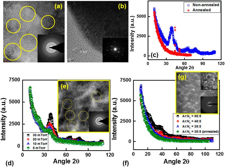
FIGURE 2. (A) Showcases a transmission electron microscopy (TEM) image of opaque WNx, accompanied by a TEM diffraction pattern located at the lower legitimate edge; (B) exhibits a TEM image of processed crystallized WNx, also accompanied by a TEM diffraction pattern at the lower precisely edge; (C) X-ray diffraction (XRD) spectrum of brittle amorphous WNx in blue, juxtaposed with the XRD spectrum of annealed WNx in red; (D) A collection of XRD spectra for WNx gasped under varying container exertion values, specifically under a gas mixture ratio of Ar:N2 at 55:5; (E) Showcases a TEM image of WNx gasped under a stress of 30 mTorr, with an inset displaying the corresponding TEM diffraction image; (F) Presents diverse XRD spectra of WNx gasped under a stress of 5 mTorr, while employing distinct air mixture ratios of Ar:N2, ranging from 55:5 to 35:5 sccm; (G) Exhibits a TEM image of WNx gasped under a stress of 5 mTorr, utilizing an air combination ratio of Ar:N2 at 35:5 sccm, accompanied by a TEM diffraction image positioned at the lower legitimate edge.
The visual representation illustrated in Figure 2A, acquired via the utilization of the High-Resolution Transmission Electron Microscopy (HRTEM) instrument, presents empirical support for the presence of a finite quantity of crystalline islands (emphasized by yellow spheres) within the surrounding amorphous framework. The manifestation of crystalline clusters is visually represented as circular formations situated in the lower right quadrant of the transmission electron microscopy (TEM) diffraction image. The initiation of the crystallization process occurs upon subjecting the material to elevated temperatures exceeding 480°C, as depicted in Figure 2B, which showcases the transmission electron microscopy (TEM) image alongside the corresponding diffraction pattern. The visual representation of the X-ray diffraction (XRD) wavelengths of amorphous WNx, obtained using the Grazing Incidence X-ray Diffraction (GI-XRD) method, is illustrated in Figure 2C. The observed broad spike within the spectrum signifies the existence of a limited number of crystalline clusters that are embedded within the amorphous bulk material. The provided image additionally portrays the X-ray diffraction (XRD) spectrum of a thermally treated crystalline substance exhibiting prominent peaks. The degree of amorphousness can exhibit a spectrum ranging from low to high, contingent upon the presence of a crystalline structure, which can range from a reduced number of crystals (low) to a complete absence of any discernible crystalline arrangement (high). The transmission electron microscopy (TEM) analysis reveals a crystalline size of approximately 5 nm. However, when applying the Scherrer formula to estimate the crystal size, it is important to acknowledge that tool broadening can be disregarded due to the nature of the measurement being conducted on a thin film rather than a powder. Consequently, the computed crystal size is expected to be around 2 nm. The anticipated outcome is that the crystalline size ascertained through transmission electron microscopy (TEM) is expected to surpass the crystalline size determined via X-ray diffraction (XRD). This is primarily attributed to the fact that the specimen thickness is below 100 nm and is exposed to a high-intensity electron beam, which induces an annealing effect and consequently augments the crystalline size.
A low degree of amorphousness is indicative of the presence of crystalline structures, whereas a high degree of amorphousness suggests the absence of any such structures. The requisite condition for the establishment of crystalline structures, a characteristic feature of metals, is the presence of elevated adatom mobility. The gaseous nitrogen (N2) within the plasma of the deposition chamber undergoes dissociation, resulting in the formation of nitrogen radicals (N). These radicals subsequently engage in chemical reactions with tungsten (W) atoms. The adatom motion is effectively suppressed as a result of this chemical reaction, resulting in the formation of WNx with an amorphous molecular configuration. Upon subjecting the material to temperatures exceeding 480°C, it is observed that the material undergoes complete crystallization, primarily attributed to the presence of crystalline WNx. Following the meticulous adjustment of the sputtering parameters, we successfully acquired amorphous metal material that exhibited a complete absence of crystalline clusters. This material was subsequently employed in the fabrication process of the nanoelectromechanical (NEM) switches. In order to successfully execute this undertaking, it is crucial to consider a multitude of factors, which include but are not confined to strain, strength, air blend proportion, distance separating the quarry to substrate, and ultimately the specific type of power utilized, specifically alternating current (AC) or direct current (DC).
In order to mitigate the displacement of adatoms during the course of our investigation, a consistent power level of 300 W was sustained, while concurrently increasing the separation between the target and the substrate. The sputtering pressure underwent a gradual reduction in four sequential increments, commencing from an initial value of 30 millitorr and concluding at a final value of 5 millitorr. Throughout this process, the proportion of Argon (Ar) gas to Nitrogen (N2) gas remained constant at a ratio of 55:5 standard cubic centimeters per minute (sccm). The X-ray diffraction (XRD) spectrum depicted in Figure 2D demonstrates that the lowest pressure conditions yielded the most amorphous structure across all samples. The transmission electron microscopy (TEM) images and diffraction patterns corresponding to the minimum pressure configuration are depicted in the inset of Figure 2E. In the course of this experimental investigation, it was ensured that the pressure remained constant at a value of 5 millitorr, while the gas mixture ratio was systematically altered in order to meticulously adjust the amorphization procedure. By modulating the Ar flow rate while maintaining a constant N2 flow rate, as depicted in Figure 2F, the optimal XRD outcome was achieved at a specific ratio of 35:5 sccm (Figure 2G [inset)]. Based on the conspicuous scarcity of crystalline clusters observed in the test sample, it can be inferred that the deposited film currently exhibits an amorphous nature, or alternatively, a quasi-state.
The deposited film underwent thermal treatment at an elevated temperature of 750°C for a duration exceeding 90 min, while being exposed to a range of gases including oxygen (O2), nitrogen (N2), and argon (Ar). Notably, the film retained its amorphous nature when subjected to the N2 and Ar atmospheres, thereby indicating its inherent rigidity. The X-ray diffraction (XRD) spectra of the WNx film subsequent to the rigorous environmental assessment is presented in Supplementary Figure S2. Upon subjecting WNx to rigorous testing utilizing a nano-indentation apparatus, the resultant Young’s modulus (E) was determined to be 300 GPa, while its hardness (H) was ascertained to be 3 GPa. The NEM switches exhibit enhanced resistance to stress and deformation due to their inherent properties of robust elasticity and hardness, alongside the absence of grain boundaries in their amorphous structure. As a consequence of this phenomenon, the durability of the device is enhanced, thereby leading to an amelioration in the contact resistance. The measurement of sheet resistance was carried out using a four-probe setup with a length of 200 cm. The measurements were conducted at two different time points: immediately following the accumulation, followed by a duration of 4 weeks in a typical atmosphere. This environment is characterized by the presence of atmospheric moisture alongside a median regular humidity of at least 70%.
The results indicate that the inclusion of nitrogen atoms within the tungsten atomic arrangement induces an amorphous structure and mitigates the propensity for native oxide formation. The density of the amorphous WNx material that has been deposited is measured to be 17.5 g cm-3. The observed density exhibits an intermediary value when compared to the densities of cubic crystalline structures, such as -W2N with a density of 16 g cm (-3), and hexagonal crystalline structures, such as -WN with a density of 18 g cm (-3). In order to mitigate the occurrence of sagging in the hanging section of the switch, a conservative tensile stress of 500 MPa has been deliberately introduced into the coating. The provided discourse does not introduce any novel data that contradicts the observed measurements. By employing the Agilent 5,500 Scanning Probe Microscope (SPM) in intermittent contact imaging mode, we have successfully ascertained the average surface roughness of the WNx layer, which encompasses a projected area of 64 square meters, to be 2.53 nm. The range exhibits considerable breadth, encompassing a maximum value of 30 nm and a minimum value approaching 0 nm. Notably, the median value is determined to be 2.31 nm, as depicted in Supplementary Figure S3. The successful prevention of micro-welding inability was accomplished by means of reducing the magnitude of energy that is stored within the working components, facilitated by the amorphous characteristics of the material and the observed smooth surface as evidenced by atomic force microscopy (AFM). Welding is a significant concern for both classic MEMS and current NEMS systems (including NEM switches). Previous studies have shown that applying a small layer of oxide to the contact surface may prevent this by increasing the contact resistance and so reducing the ON current (Chen et al., 2012). However, the switch’s performance rapidly degrades due to the process of the thinner layer of oxide undergoing combustion during functional phases. The new amorphous WNx material in NEM switch design with a smooth contact surface prevents charges from building up at sudden spikes, and the increased molecular bonding due to the high atomic density prevents further oxidation. As a result, this contributes to establishing a modest contact resistance to prevent excess charge flow while not assisting in the creation of native oxide to maintain consistent performance throughout the switch lifespan.
Ablation and aggravation pose significant challenges within the context of NEM switching. Although infrequent in hard materials, it is noteworthy that their elevated electrical resistance can impede the efficiency of switching processes and result in the generation of excessive heat, ultimately culminating in the occurrence of welding. Thin oxide coatings encounter similar challenges, encompassing the degradation of materials throughout successive operational cycles. Friction emerges as a notable quandary when endeavoring to expand the scale of NEM (nanoelectromechanical) switches for intricate circuitry. The phenomenon known as stiction arises as a consequence of an insufficiency in the mechanical restoring force. In order to mitigate the phenomenon of stiction, a number of scholars have put forth the proposition of utilizing a substantial pull-back voltage at the electrode that is situated in opposition. Due to the deleterious effects of high voltage operation on operational speed and switch reliability, it is evident that this particular course of action lacks practicality. The Young’s modulus of amorphous WNx is observed to be 300 GPa, a value that is notably elevated, thereby suggesting a substantial spring constant. Upon the cessation of the electrical pulling force (Fe), the mechanical force (Fm) becomes adequate to effectuate the retraction of the active element, thereby obviating the necessity for high voltage pull back.
The occurrence of stiction can be attributed to the combined effects of the van der Waals force and the Casimir force, as elucidated by prior scholarly inquiries (Duan and Rach, 2013). One potential approach for addressing this matter involves the implementation of a mechanical restoring force of sufficient magnitude to effectively counteract the accumulated stiction force. Simultaneously, given their precise proportionality, it is imperative that this restorative force does not exhibit sufficient strength to elevate the pull-in voltage, denoted as Vpi. Due to the relatively diminished Young’s modulus, it can be observed that NEM (nano-electromechanical) switches constructed from silicon material exhibit an increased susceptibility to stiction, with a recorded value of approximately 160 GPa. On the contrary, materials that possess a significant Young’s modulus, including opaque carbon, carbon nanotubes (CNT), and silicon carbide (SiC), demonstrate minimal concerns associated with stiction. The material known as WNx, which lacks a definite crystalline structure, demonstrates a Young’s modulus that falls between the extremes. This characteristic allows it to effectively overcome the problem of stiction that is frequently encountered in NEM (nanoelectromechanical) switches made from silicon-based materials. Importantly, the use of WNx eliminates the need for employing high working voltages, which is a requirement when utilizing carbon-based materials. The occurrence of mechanical inability in NEM switches can be attributed to inherent crystal structural imperfections. This failure happens due to the presence of a cluster border, which produces fracture, deformation, material fatigue, or a combination of the above. The interfaces between the grains are indeed the material’s weakest point, and fractures develop at these interfaces. This flaw significantly reduces the device’s lifespan. In order to rectify the aforementioned inadequacy and flaw inherent in poly-crystalline material, it is imperative that the material employed for the construction of NEM switches be considered either mono-crystalline or amorphous in nature. Due to the inherent limitations of contemporary CMOS processes, the production of mono-crystalline metal remains unattainable. Consequently, the utilization of amorphous metals, such as WNx, may assume a pivotal significance in addressing this predicament. Consequently, our subsequent objective entailed the utilization of a WNx-based nano-ribbon as the primary constituent material for a two-terminal nanoelectromechanical (NEM) switch.
When considering the design process, it is imperative to acknowledge that the NEM switch length encompasses two significant implications. Two key observations can be made regarding the relationship between length and certain performance metrics. Firstly, it has been observed that a decrease in length is associated with an increase in operation speed. By reducing the length of the NEM switch, it is possible to shorten the amount of time that is necessary for the cantilever to experience displacement. Because of the decrease in length, there is a possibility that switching periods may be expedited, which would ultimately lead to an increase in the NEM switch’s overall velocity. Secondly, an increase in length is correlated with a decrease in pull-in voltage. It is commonly observed that shorter lengths of switches generally necessitate a reduced voltage in order to achieve the pull-in phenomenon, thereby rendering the switch more energy-efficient in nature. The establishment of this relationship can be attributed to the underlying principles of fundamental physics that govern the electrostatic forces observed in NEM (Nano-Electro-Mechanical) devices as illustrated in Eq. 1. The alteration in the dimensions of the cantilever beam induces corresponding modifications in the capacitance and electrostatic forces existing between the cantilever and electrode. Increased length typically results in increased capacitance, thereby yielding diminished pull-in voltages.
• Where, ϵ0 is the vacuum permittivity (8.854 × 10⁻¹² F/m8.854 × 10−12F/m), ϵr is the relative permittivity of the material between the plates, L is the length of the cantilever beam, Vbias is the bias voltage applied.
The observed phenomena indicate a positive correlation between the Young’s modulus and wideness of the material, and both the velocity and pull-in voltage. Conversely, a negative correlation is observed between the cantilever length and both the velocity and pull-in voltage. To optimize the performance characteristics of the NEM switch, it is advisable to employ a design strategy that entails reducing the dimensions of all components, except for the length, with the aim of minimizing the pull-in voltage while simultaneously increasing the quality factor and resonant frequency. In a general sense, it can be observed that the temporal duration required for a switching event exhibits a negative correlation with the magnitude of the pull-in voltage. The achievement of optimal fabrication of nanoelectromechanical (NEM) switches is contingent upon the simultaneous existence of two critical factors: a significantly elevated Young’s modulus and dimensions at the nano-scale level.
To fulfill the aforementioned criteria, the utilization of amorphous tungsten nitride (WNx) was employed to fabricate a vertically actuated, cantilever-type nanoelectromechanical (NEM) switch featuring a double clamp configuration. The fabrication process of the bottom electrode involved the deposition of a 30 nm thin film of amorphous WNx onto a heavily doped (50 m.cm) prime grade n-type 4″silicon (100) wafer, which was utilized as the gate. A protective layer of silicon dioxide (SiO2) with a thickness of 300 nm was successfully deposited through the utilization of plasma-enhanced chemical vapourdeposition (PECVD) technique. The fabrication process of the active layer in a nano-membrane composed of amorphous WNx material, with a thickness of 100 nm, was successfully accomplished, as detailed in previous literature. The active layer was shaped utilizing a UV contact aligner, with the aid of positive tone photoresist. A nano-ribbon was fabricated through the process of reactive ion etching on an amorphous WNxnano-membrane. The resulting nano-ribbon possesses dimensions of 100 nm in thickness, 2 µm in width, and 12 µm in length. The fabrication process was conducted at a temperature of 10°C and a pressure of 20 mTorr, utilizing a plasma generated from a gas mixture of SF6 and Ar at flow rates of 15/5 sccm, respectively. The nano-ribbon features an air gap measuring 300 nm. The formation of the free-standing cantilever structure was achieved through the process of etching the sacrificial layer, which consisted of plasma-enhanced chemical vapor deposition (PECVD) silicon dioxide (SiO2), using hydrofluoric acid (HF) in its vapor state.
Figure 3A illustrates the cantilever within amorphous structure molecules, serving as a means of demonstration. Conversely, Figure 3B portrays the stationary and activated orientations of the vertical NEM switch. Figure 3 illustrates a scanning electron microscopic (SEM) image (c). The results of the COMSOL simulation (d, e) are depicted in Figures 3, 4. The observed Vpi values surpass the levels that were theoretically estimated. The Vpi voltage represents a singular mathematical entity within the solution, which, when encountered during simulation, induces a state of theoretical instability in the system’s operation. Upon reaching this particular stage of the simulation operation, error notifications are presented to the user, subsequently leading to the termination of the procedure. As a result, the simulation must revolve around the Vpi, yielding an adequate approximation to the Vpi (Elshurafa et al., 2013). The figures denoted as 3 (d, e) present the 3-dimensional device layout of the simulated NEM switch. The cantilever deflection curve for various gate voltages (Vg) is illustrated in Figure 3E. A positive correlation can be observed between the gate voltage and the magnitude of beam deflection. As the gate voltage (Vg) approaches the pinch-off voltage (Vpi), the deflection distance of the cantilever exhibits a significant escalation, ultimately resulting in the cantilever’s collision with either the gate or the drain at Vg = Vpi. Upon reaching a certain threshold, denoted as Vg, the switch in question exhibits a state of instability, leading to the manifestation of an error message within the simulation software known as COMSOLTM. This error message signifies the attainment of the boundary pole, thereby indicating the occurrence of this particular phenomenon.

FIGURE 3. (A) Vertically actuated doubly clamped NEM switch with amorphous structure molecules; (B) 3D layout of vertically actuated doubly clamped NEM switch in rest and in motion; (C) SEM picture of aWNx integrated vertically actuated doubly clamped NEM switch after trillion cycles run (discussed later); (D) model of the same switch for COMSOL simulation; (E) deflection profile of the NEM switch at different Vg.
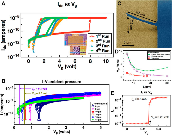
FIGURE 4. (A) Transfer (I–V) curve for 4 consecutive pull-in operation of a laterally actuated singly clamped two terminals NEM switch. [Inset: SEM image of the fabricated switch]; (B) transfer (I–V) curve after multiple runs of vertically actuated doubly clamped two terminals NEM switches of multiple cantilever lengths.; (C) Pertains to a singular clamped ribbon configuration, characterized by a cantilever arrangement, which exhibits an upward curvature as a consequence of a stress gradient.; (D) Pull-in voltages vs. cantilever length, calculated and experimentally measured values with and without stress gradient; (E) Transfer (I–V) curve of a laterally actuated three terminals NEM switch (l = 16 μm, g = 100 nm, w = 180 nm, t = 300 nm) shows sharp transition (turn-on).
The transfer (I-V) characterization of a single clamped lateral NEM switch fabricated from WNx is illustrated in Figure 4A, as shown in the inset. The observed phenomenon displays the characteristic hysteresis commonly observed in similar transitions. The decrease in the slope of the current-voltage (I-V) curve can be attributed to the degradation of the cantilever’s edge corner, which serves as the initial point of contact. This deterioration occurs as a result of the mechanical hammering effect that takes place following the completion of the first cycle. In successive cycles, it is observed that edge contact alone fails to facilitate the efficient conduction of high currents, primarily owing to the elevated resistance encountered. The phenomenon of hammering induces detrimental effects on the contact surface, leading to a subsequent reduction in the effective contact area. This reduction in contact area consequently results in an increase in resistance. Nevertheless, as the Vg value is elevated, there is a concomitant increase in the contact area, thereby resulting in a heightened flow of electric current.
The rationale underlying the gradual increase in electrical current at the Vpi can be attributed to a number of factors. The aforementioned scenario does not pertain to the double clamped NEM switch, as the contact point in this particular instance does not possess the attributes of a free corner. Consequently, it does not undergo deterioration and exhibits commendable endurance characteristics. It can be posited that the structural integrity of a singly clamped NEM (nanoelectromechanical) switch is comparatively more vulnerable when juxtaposed with its doubly clamped counterpart, primarily attributable to the presence of a reduced anchoring mechanism. The absence of discernible hysteresis is demonstrated by a collection of I-V curves depicted in Figure 4B, which correspond to different lengths of cantilevers spanning a range of 6–18 µm. The ratio between the observed value of Vpi and the estimated value of Vpi falls within a range of 60%. The value has been adjusted. Moreover, it is evident from the aforementioned diagram that the pullout voltage (Vpo) is equivalent to the input voltage (Vpi). Vpo and Vpi are equal, indicating that the NEM switch operates adiabatically due to the absence of hysteresis power loss (Mayet et al., 2015). The manifestation of hysteresis behavior in the mechanical functioning of NEM switches is a consequence of the cessation of electrostatic force (Fe), as a result of the presence of adhesion force (Fadh). The adhesion force is comprised of the combined effects of van der Waal force and Casimir force. The observed augmentation in the Young’s modulus of amorphous WNx leads to a commensurate amplification in the mechanical restoring force (Fm). This finding aligns with previous investigations conducted on SiC-based materials and carbon nanotubes (CNT). The proportionality between Hook’s constant (k) and the Young’s modulus is well-established. In the specific case of WNx, it is noteworthy that the modulus is threefold higher than that of Silicon. However, it is important to acknowledge that the restoring force is relatively minuscule due to the diminutive mechanical displacement (x) involved. Due to the prevailing circumstances, it is evident that the aggregate restorative force in our given scenario is of considerable magnitude.
In Figure 4B, the curves are coarse due to multiple switching resulting into a set of IV curves which are not absolutely identical. Tunneling analysis was not performed because the generated I-V curve is for mechanical contact of NEM switch. If the beam is pulled and stick to the opposing static electrode, and the generated I-V curve is the result of tunneling effect, then the generated I-V curve should be identical for all different lengths of beam. This is not the case in our experiment. Different lengths generated different Vpi and different I-V curves are consistent for consecutive experiments. A metal insulator metal (MIM) tunneling experiment has been conducted by other group (Kumari and Angira, 2022), where the insulator thickness is around 10 nm and tunneling voltage is around 5 V. In our experiment the insulator beneath the probe pad is 100 nm. If the voltage is for tunneling then it requires more than 50 V to tunnel such thick oxide. Furthermore, there is no insulator between the cantilever and the gate nor native oxide as the amorphous metal prevent such oxide formation.
The graphicalrepresentation in Figure 4C illustrates the characteristic of an upwardlyinclined curve pertaining to a cantilever of the single clamped ribbon type. The resultant bending moment (M) servesas a contributingfactor to the mechanicalrestoring force (Fm) by effectivelycounteracting the adhesion force. The utilization of Eq. 2 isemployed in the computation of the resultant bending moment.
Here, M is the bending moment, E is the Young’s modulus, w is the cantilever beam width, t is the film thickness, l is the cantilever length, and Z is the cantilever tip deflection distance.
The spatial separation observed between the cantilever and the gate in this context exhibits a direct correlation with the magnitude of the cantilever’s length. The disparity will inevitably expand in direct proportion to the elongation of the cantilever, owing to the presence of a stress gradient. The data presented in Figure 4D exhibits a positive correlation between the cantilever length and the pull-in voltage. Specifically, as the cantilever length extends to 18 μm, there is a discernible rise in the pull-in voltage. This can be attributed to the concurrent increase in the gap between the cantilever and the substrate. In the current phase of development, the implementation of twin clamped vertical NEM switches has been employed. Eqs 3, 4 delineate the mathematical expressions encapsulating the mechanical restoring force (Fm) in both the single clamped and double clamp scenarios. The aforementioned equations yield the observation that the flexural stiffness force (Fm) of double clamped nanoelectromechanical (NEM) switches is 64 times greater than that of single clamped NEM switches.
• For the single clamped NEMS:
• For double clamp NEMS:
Where g is the gap between the cantilever and the gate.
Figure 4B shows hysteresis-free switching due to the high Fm and high moment (M) overriding the Fadh. When compared to double-clamped lateral NEM switches made from WNx, the mechanical restoring force is 64 times lower and there is no surface tensile stress (M) to further influence this hysteresis-less behavior. Beam and drain gap is larger than one-third of the space between beam and gate. Beam-to-drain adhesion forces are unaffected by differences in gap size, it is governed by the molecular structure of the surface and the nanoscale gap between the two surfaces. When the adhesion force (the total of various forces) and the pull-in electrostatic forces are larger than the mechanical restoring force, the hysteresis occurs. It is independent of the drain gap. If the drain gap is high (>1/3 gate gap) then the mechanical restoring force will be greater but it will not be effective as the spring constant is low as in the case of Si poly crystalline. However, in amorphous WNx, the longer travel distance will make stronger restoring force as the spring constant k is higher. Thus, the hysteresis have been eliminated by having moderately rough contact surface and high spring constant which yields into lower adhesion force and higher restoring force. Simultaneously, this is advantageous in producing reduced pull-in voltage, the researchers successfully conducted measurements on the sub-0.3 pull-in voltage, specifically at a value of 0.28 V. Additionally, they achieved a high Ion/Ioff ratio of approximately 103. (Figure 4E). A doubly clamped vertically actuated switch may undergo additional Vpi reduction by decreasing the air gap between the gate and the cantilever body and increasing the cantilever length. It is to be noted that the drain voltage is 0.5 V which yield 0.5 mA (I = V/R = 0.5/1kΩ = 0.5 mA). Furthermore, the drain voltage is not much greater than the pull-in voltage. As the pull-in force is represented as, the influence of electrode length is no less substantial than the effect of potential difference:
The gate electrode length is 15× > drain electrode length while the Vd is 2×Vpin. Hence, the gate voltage is the dominant voltage in pulling the cantilever, but the drain voltage is not totally negligible.
The cantilever resistance for a 12 µm switch is determined to be 0.2 kՈ, while for a 10 µm switch it is found to be 0.17 kՈ. However, it is noteworthy that the measured resistance falls below the threshold of 5 kՈ. The resistance was determined by employing the resistivity obtained through the utilization of a 4-point probe meter, in conjunction with the dimensions of the switch. It is worth noting that the resistance is directly proportional to the resistivity and length, while being inversely proportional to the cross-sectional area. The summation of the cantilever resistance and the contact resistance yields the overall resistance. The contact resistance is approximately 4.8 kilo-ohms. The resistance exhibited in the contract is visually represented in Figure 4B as an inset. It is observed to be of the magnitude of a few kiloohms in the contact state. Notably, there is no discernible increase in resistance even after an extensive number of cycles, which will be elaborated upon in the subsequent discussion. It is imperative to acknowledge that the design of the switch does not exert any influence on the low contact resistance.
In the context of Figure 5A, the illustrated step entails the establishment of a linkage between the device under examination and two distinct apparatuses, namely, a function generator and an oscilloscope. This connection is established with the intention of evaluating the device’s robustness and longevity. The diagram provided depicts a streamlined arrangement of a Nano-Electro-Mechanical (NEM) switch, wherein an input voltage (Vin) is generated by a function generator, and an output voltage (Vout) is measured using an oscilloscope. The schematic representation of the circuit in question is depicted in Figure 1A, wherein the function generator is interconnected with the Source (S) terminal, while the oscilloscope is linked to the Gate (G) terminal (G). The contact resistance, referred to as Rc, and the metal resistance, denoted as Rm, exhibit magnitudes that are approximately within the range of a few kilo-ohms. The aforementioned resistances are arranged in a series configuration alongside the internal resistance of the oscilloscope, which exhibits a magnitude approximately equivalent to 1 mega-ohm. The waveforms of the input voltage, denoted as Vin, and the output voltage, denoted as Vout, are illustrated in Figure 5B in accordance with the measurements performed. Based upon the information provided, one can deduce that the NEM switch currently under examination demonstrates a time delay in switching operations amounting to 30 ns, specifically when operating at a frequency of 1 MHz. The aforementioned characteristic implies that the upper limit of the operational frequency for the NEM switch under consideration is projected to be 2.5 MHz.
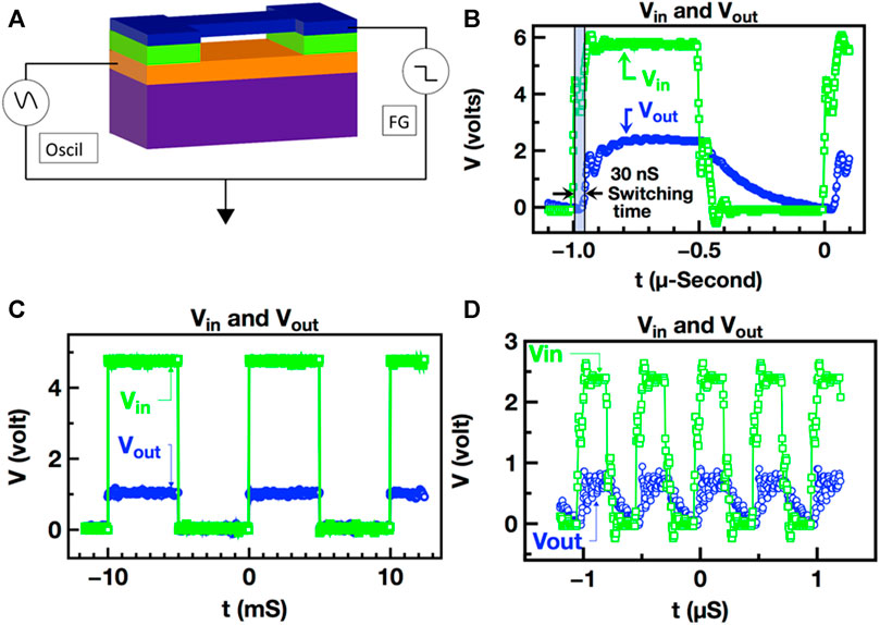
FIGURE 5. (A) A straightforward illustration of an electrical schematic involving a Nano-Electro-Mechanical (NEM) switch that is interconnected with a function generator as Vin and oscilloscope for Vout; (B) input and output voltage signal at 1 MHz shows the switching time of 30 ns; (C) input and output functions at low frequency 100 Hz illustrate a perfect square wave contour; (D) input and output functions at a high frequency 2.5 MHz illustrate a higher distortion in square wave profile.
The phenomenon of latency absence has been duly noted in the utilization of the NEM switch at a diminished velocity of 10 milliseconds, a verifiable observation that has been substantiated by prior scholarly investigations. The Vin and Vout curves demonstrate the occurrence of cantilever bounce and settling time lag when the pull-in condition is reached. The evaluation of the device’s quality and speed can be ascertained through an analysis of the duration necessary for the gadget to attain a state of stability. The materials encompassing tungsten and its alloys manifest noteworthy attributes, including heightened density and hardness. As a result, it can be observed that these materials exhibit a measure of excellence or superiority in a given context, a prolonged damping time, and an increased pull-in voltage. The temporal attributes of switching and settling times are illustrated in Figure 5B, wherein it is observed that the aforementioned durations approximate 30 and 10 nanoseconds, respectively. Wrought-iron devices demonstrate a range of quality factors spanning from 60 to 100. There exists a positive correlation between the quality factor and the duration of the settling period. The employment of kinematic formulae, as exemplified in Eq 6, fulfills the objective of determining the magnitude of the velocity at the moment of impact.
The observed impact velocity is 13 m per second. Kinetic energy decreases with the square of the velocity. Therefore, less switching power and slower top speeds might be expected from a smaller drain gap (impact velocity). When a NEM switch is activated, The repeated application of force on the source switch against the drain electrode has the potential to result in detrimental effects on the contact area. This may manifest as an elevation in contact resistance and a reduction in the overall lifespan of the component. However, the natural oxide coating on the source and drain surfaces is removed during hammering, resulting in a paradoxical reduction in contact resistance. Neither of these opposing events is desirable when the NEM switch is running continuously. It is important to keep in mind that micro- and nano-scale switches may have differing material characteristics. An incredible 8 trillion cycles have been accomplished by our NEM switch over a 10-day period at the frequency of 10 MHz, and the switch continues to function at its peak efficiency level. A 10-day SEM picture and I-V curve (Figure 3C) are identical to those obtained before to initiation of the endurance test. In the same test, this article uses gold-plated NEM switches (Au) and they failed after a million cycles before blowing out (see Figure 1H). Figure 5C depicts the waveforms of the input and output voltages (a) at a low frequency of 100 Hz, showing that the switch produced input and output voltages with perfect square wave profiles. At a frequency of 2 MHz, Figure 5D depicts the same waveform as Figure 5B. In contrast to a device made from amorphous WNx, the output waveform profile is altered and destroyed. Due to the wide crystalline barriers that restrict the nano-scaling and produce internal tension, gold (Au) exhibits operational flaws such as electrode wear or active element fractures and fatigue.
Due to its high Young’s modulus (300 GPa) and compact dimensions (100 nm thickness and 300 nm air-gap), the amorphous WNx-based nano-ribbon-shaped doubly clamped NEM switch in this paper switches at Vpi = 0.3 V. Young’s modulus increases mechanical restoring force (Fm), which counteracts van der Waal’s and Casimir forces. This minimizes the risk of permanent stiction, especially in non-volatile forms. Endurance tests in air, O2, N2, Ar, high, and low vacuum settings proved the NEM switch’s effectiveness. Under vacuum, endurance performance was better than small ambient operating cycles. The authors believe this can be improved. Because of the smooth surface and high hardness supplied by closed-packed atomic density created by oxidation resistance, high current density induced excessive heating in the contact zone, preventing mechanical welding or electrical fusing. The aforementioned technique has 8 trillion switching cycles, exceeding any previously documented NEM switch with similar pull-in and pull-out voltage. This astounding breakthrough removes hysteresis loss and delay. Researchers found a 0.5 mA boost in ON current and a relatively low ON resistance of 5kՈ. The authors found that nanostructuring amorphous metals like WNx can create “ideal” NEM switches. This work advances beyond existing research limits, setting a new norm for nanoelectromechanical systems (NEMS) switch durability. Innovative use of this material increases mechanical durability and opens up promising applications requiring prolonged and reliable switch performance. The contribution above marks a major step toward fully using nanoscale technologies in several technical fields.
The original contributions presented in the study are included in the article/Supplementary Material, further inquiries can be directed to the corresponding authors.
AM: Conceptualization, Formal Analysis, Methodology, Software, Writing–original draft. MM: Methodology, Software, Writing–original draft. HA: Methodology, Software, Writing–original draft. FK: Conceptualization, Methodology, Writing–original draft. EE: Conceptualization, Visualization, Writing–original draft.
The author(s) declare financial support was received for the research, authorship, and/or publication of this article. The authors extend their appreciation to the Scientific Council at King Khalid University for funding this work. The Authors are also thankful to Prof. Fadi Kurdahi, Center of Embedded and Cyber-Physical Systems (CECS), Lab and Prof. Amit Lal, SONIC Lab of Cornell University for their valuable feedbacks. I declare no competing financial interest. We acknowledge support by the German Research Foundation Projekt-Nr. 512648189 and the Open Access Publication Fund of the Thueringer Universitaets- und Landesbibliothek Jena.
The authors extend their appreciation to the Scientific Council at King Khalid University for funding this work. The Authors are also thankful to Prof. Muhammad M Hussain, Integrated Nanotechnology Lab, and Integrated Disruptive Electronic Applications (IDEA) Lab and Prof. Amit Lal, SONIC Lab of Cornell University for their valuable feedbacks.
The authors declare that the research was conducted in the absence of any commercial or financial relationships that could be construed as a potential conflict of interest.
All claims expressed in this article are solely those of the authors and do not necessarily represent those of their affiliated organizations, or those of the publisher, the editors and the reviewers. Any product that may be evaluated in this article, or claim that may be made by its manufacturer, is not guaranteed or endorsed by the publisher.
The Supplementary Material for this article can be found online at: https://www.frontiersin.org/articles/10.3389/fmats.2023.1337925/full#supplementary-material
Addonizio, M. L., Castaldo, A., Antonaia, A., Gambale, E., and Iemmo, L. (2012). Influence of process parameters on properties of reactively sputtered tungsten nitride thin films. J. Vac. Sci. Technol. A Vac. Surfaces, Film. 30 (3), 031506. doi:10.1116/1.3698399
Alqahtani, M. S., Abbas, M., Abdulmuqeet, M., Alqahtani, A. S., Alshahrani, M. Y., Alsabaani, A., et al. (2022). Forecasting the post-pandemic effects of the SARS-CoV-2 virus using the bullwhip phenomenon alongside use of nanosensors for disease containment and cure. Mater 15 (14), 5078. doi:10.3390/MA15145078
As Bale, S. R. S. H., Reddy, S. V., and Huddar, S. A. (2020). Electromechanical characterization of Nitinol based RF MEMS switch. Mater Today Proc. 27, 443–445. doi:10.1016/j.matpr.2019.11.263
Auciello, O., and Aslam, D. M. (2021). Review on advances in microcrystalline, nanocrystalline and ultrananocrystalline diamond films-based micro/nano-electromechanical systems technologies. J. Mat. Sci. 56 (12), 7171–7230. doi:10.1007/s10853-020-05699-9
Chen, Y., Nathanael, R., Jeon, J., Yaung, J., Hutin, L., and Liu, T. J. K. (2012). Characterization of contact resistance stability in MEM relays with tungsten electrodes. J. Microelectromechanical Syst. 21 (3), 511–513. doi:10.1109/JMEMS.2012.2186282
Chong, S., Lee, B., Mitra, S., Howe, R. T., and Wong, H. S. P. (2012). Integration of nanoelectromechanical relays with silicon nMOS. IEEE Trans. Electron Devices 59 (1), 255–258. doi:10.1109/TED.2011.2172946
Duan, J. S., and Rach, R. (2013). A pull-in parameter analysis for the cantilever NEMS actuator model including surface energy, fringing field and Casimir effects. Int. J. Solids Struct. 50 (22–23), 3511–3518. doi:10.1016/J.IJSOLSTR.2013.06.012
Elshurafa, A. M., Salama, K. N., and Ho, P. H. (2013). Modeling and fabrication of an RF MEMS variable capacitor with a fractal geometry. Proc. - IEEE Int. Symp. Circuits Syst., 2711–2714. doi:10.1109/ISCAS.2013.6572438
Fang, W., et al. (2013). “CMOS MEMS: a key technology towards the More than Moore era,” in Transducers Eurosensors XXVII 17th Int. Conf. Solid-State Sensors, Spain, 16-20 June 2013 (Actuators Microsystems, TRANSDUCERS EUROSENSORS), 2513–2518. doi:10.1109/TRANSDUCERS.2013.6627317
Feng, P. X. L., Wang, Z., Lee, J., Yang, R., Xuqian Zheng, , Keliang, H, et al. (2015). Two-dimensional nanoelectromechanical systems (2D NEMS) via atomically-thin semiconducting crystals vibrating at radio frequencies. Tech. Dig. - Int. Electron Devices Meet. IEDM 2015, 8.1.1–8.1.4. doi:10.1109/IEDM.2014.7047008
Gu, X. W., Jafary-Zadeh, M., Chen, D. Z., Wu, Z., Zhang, Y. W., Srolovitz, D. J., et al. (2014). Mechanisms of failure in nanoscale metallic glass. Nano Lett. 14 (10), 5858–5864. doi:10.1021/nl5027869
Hähnlein, B., Kovac, J., and Pezoldt, J. (2017). Size effect of the silicon carbide Young’s modulus. Phys. Status Solidi Appl. Mat. Sci. 214 (4), 1600390–1600421. doi:10.1002/pssa.201600390
Herrera-Martinez, A. I., Khotiaintsev, S., and Timofeyev, V. I. (2020). Electromechanical analyses of 1 x n MEMS-based optical switch with microplate reflector. IEEE 40th Int. Conf. Electron. Nanotechnol. ELNANO 2020 - Proc. 2020, 864–868. doi:10.1109/ELNANO50318.2020.9088797
Hr Ansari, M. T., and Behnam Taghaddosi, M. (2019). Optimization and development of the RF MEMS structures for low voltage, high isolation and low stress. Analog. Integr. Circ. Sig Process 101 (3), 659–668. doi:10.1007/s10470-019-01549-0
Koul, S. K., and Dey, S. (2022). Micromachined metamaterial inspired switches. Lect. Notes Electr. Eng. 859, 293–325. doi:10.1007/978-981-16-9443-1_10/COVER
Kumari, R., and Angira, M. (2022). FEM simulation and material selection for enhancing the performance of a RF-MEMS capacitive switch. J. Comput. Electron August, 814–825. doi:10.1007/s10825-022-01905-w
Kurmendra, H., and Kumar, R. (2021a). A review on RF micro-electro-mechanical-systems (MEMS) switch for radio frequency applications. Microsyst. Technol. 27 (7), 2525–2542. doi:10.1007/s00542-020-05025-y
Kurmendra, H., and Kumar, R. (2021b). Investigations on beam membrane and dielectric materials using Ashby’s methodology and their impact on the performance of a MEMS capacitive switch. Microsyst. Technol. 27 (12), 4269–4289. doi:10.1007/S00542-021-05220-5
Kurmendra, H., and Kumar, R. (2022). RF micro-electro-mechanical system (MEMS) capacitive switch performance parameters and improvement strategies. Microsyst. Technol. 28, 1765–1783. doi:10.1007/S00542-022-05324-6
Kurmendra, H., and Kumar, R. (2019). MEMS based cantilever biosensors for cancer detection using potential bio-markers present in VOCs: a survey. Microsyst. Technol. 25 (9), 3253–3267. doi:10.1007/s00542-019-04326-1
Lee, J. O., Song, Y. H., Kim, M. W., Kang, M. H., Oh, J. S., Yang, H. H., et al. (2012). A sub-1-volt nanoelectromechanical switching device. Nat. Nanotechnol. 8 (1), 36–40. doi:10.1038/nnano.2012.208
Loh, O. Y., and Espinosa, H. D. (2012). Nanoelectromechanical contact switches. Nat. Nanotechnol. 7 (5), 283–295. doi:10.1038/nnano.2012.40
Lu, S. C., Tsai, C. P., Huang, Y. C., Du, W. R., and Li, W. C. (2018). Surface condition influence on the nonlinear response of MEMS CC-beam resoswitches. IEEE Electron Device Lett. 39 (10), 1–1603. doi:10.1109/LED.2018.2865956
Mayet, A., Smith, C. E., and Hussain, M. M. (2013). Energy reversible switching from amorphous metal based nanoelectromechanical switch. Proc. IEEE Conf. Nanotechnol., 366–369. doi:10.1109/NANO.2013.6720965
Mayet, A. M., Hussain, A. M., and Hussain, M. M. (2015). Three-terminal nanoelectromechanical switch based on tungsten nitride—an amorphous metallic material. Nanotechnology 27 (3), 035202. doi:10.1088/0957-4484/27/3/035202
Mk Bonthu, A. S., and Sharma, A. K. (2018). An investigation of dielectric material selection of RF-MEMS switches using Ashby’s methodology for RF applications. Microsyst. Technol. 24 (4), 1803–1809. doi:10.1007/s00542-017-3539-x
Nakajima, H., Chang, T. F. M., Chen, C. Y., Konishi, T., Machida, K., Toshiyoshi, H., et al. (2017). A study on young’s modulus of electroplated gold cantilevers for MEMS devices. 2017 IEEE 12th Int. Conf. Nano/Micro Eng. Mol. Syst. NEMS, 264–267. doi:10.1109/NEMS.2017.8017021
Nawaz, H., Masood, M. U., Saleem, M. M., Iqbal, J., and Zubair, M. (2020). Surface roughness effects on electromechanical performance of RF-MEMS capacitive switches. Microelectron. Reliab. 104, 113544. doi:10.1016/J.MICROREL.2019.113544
Parsa, R., Lee, W., Shavezipur, M., Provine, J., Maboudian, R., Mitra, S., et al. (2013). Laterally actuated platinum-coated polysilicon NEM relays. J. Microelectromechanical Syst. 22 (3), 768–778. doi:10.1109/JMEMS.2013.2244779
Riverola, M., Vidal-Álvarez, G., Sobreviela, G., Uranga, A., Torres, F., and Barniol, N. (2016a). Dynamic properties of three-terminal tungsten CMOS-NEM relays under nonlinear tapping mode. IEEE Sens. J. 16 (13), 5283–5291. doi:10.1109/JSEN.2016.2561321
Ruzziconi, L., Jaber, N., Kosuru, L., and Younis, M. I. (2022). Activating internal resonance in a microelectromechanical system by inducing impacts. Nonlinear Dyn. 2022, 1109–1127. doi:10.1007/S11071-022-07706-X
Saleem, M. M., and Nawaz, H. (2019). A systematic review of reliability issues in RF-MEMS switches. Micro Nanosyst. 11 (1), 11–33. doi:10.2174/1876402911666190204113856
Shen, X., Wu, K., Sun, H., Sang, L., Huang, Z., Imura, M., et al. (2021). Temperature dependence of Young’s modulus of single-crystal diamond determined by dynamic resonance. Diam. Relat. Mat. 116, 108403. doi:10.1016/J.DIAMOND.2021.108403
Shukla, N. K., Mayet, A. M., Vats, A., Aggarwal, M., Raja, R. K., Verma, R., et al. (2022). High speed integrated RF–VLC data communication system: performance constraints and capacity considerations. Phys. Commun. 50, 101492. doi:10.1016/J.PHYCOM.2021.101492
Tahir, M. A. R., Saleem, M. M., Bukhari, S. A. R., Hamza, A., and Shakoor, R. I. (2021). An efficient design of dual-axis MEMS accelerometer considering microfabrication process limitations and operating environment variations. Microelectron. Int. 38 (4), 144–156. doi:10.1108/mi-02-2021-0023
Tian, W., Zhang, X., Chen, Z., and Ji, H. (2016). A review of graphene on NEMS. Recent Pat. Nanotechnol. 10 (1), 3–10. doi:10.2174/187221051001160322151412
Tsai, C.-P., and Li, W.-C. (2022). “CMOS-MEMS vibro-impact devices and applications,” Front. Mech. Eng., vol. 8, no pp. 1–9. doi:10.3389/fmech.2022.898328
Keywords: nanoelectromechanical switch, amorphous metal, symmetrical, tungsten nitride, endurance, casimir force
Citation: Mayet AM, Muqeet MA, Alhashim HH, Kurdahi F and Eftekhari-Zadeh E (2024) Sub-0.3 volt amorphous metal WNx based NEMS switch with 8 trillion cycles. Front. Mater. 10:1337925. doi: 10.3389/fmats.2023.1337925
Received: 13 November 2023; Accepted: 31 December 2023;
Published: 12 January 2024.
Edited by:
Chuan Li, National Yang Ming Chiao Tung University, TaiwanReviewed by:
Preeti Gupta, Leibniz Institute for Solid State and Materials Research Dresden (IFW Dresden), GermanyCopyright © 2024 Mayet, Muqeet, Alhashim, Kurdahi and Eftekhari-Zadeh. This is an open-access article distributed under the terms of the Creative Commons Attribution License (CC BY). The use, distribution or reproduction in other forums is permitted, provided the original author(s) and the copyright owner(s) are credited and that the original publication in this journal is cited, in accordance with accepted academic practice. No use, distribution or reproduction is permitted which does not comply with these terms.
*Correspondence: Abdulilah Mohammad Mayet, YW1heWV0QGtrdS5lZHUuc2E=; Ehsan Eftekhari-Zadeh, ZS5lZnRla2hhcml6YWRlaEB1bmktamVuYS5kZQ==
Disclaimer: All claims expressed in this article are solely those of the authors and do not necessarily represent those of their affiliated organizations, or those of the publisher, the editors and the reviewers. Any product that may be evaluated in this article or claim that may be made by its manufacturer is not guaranteed or endorsed by the publisher.
Research integrity at Frontiers
Learn more about the work of our research integrity team to safeguard the quality of each article we publish.