 Cristina Plamadeala
 Sebastian Lifka
 Gerda Buchberger
 Werner Baumgartner
 Johannes Heitz1
- 1Institute of Applied Physics, Johannes Kepler University Linz, Linz, Austria
- 2Institute of Biomedical Mechatronics, Johannes Kepler University Linz, Linz, Austria
In this paper we present polymer surfaces inspired by the calamistrum of cribellate spiders. The calamistrum resembles a micro-comb with a finger-print-like nanorippled topography, which allows cribellate spiders to handle and process nanofibers, without sticking to them. Due to its morphology, the calamistrum has a reduced surface for contact with the nanofibers, which therefore reduces the adhesive forces. Three different types of structured surfaces were prepared: nanostructured surfaces (ripples), microstructured surfaces (lines), and a combination of micro- and nanostructured surfaces (lines superimposed with ripples). Polymer lines were created using UV mask lithography. Nanoripples, i.e., laser-induced periodic surface structures, were fabricated by exposure to a KrF* laser beam. Nanofibers were produced and deposited onto each sample by electrospinning. To quantify each samples’ adhesiveness, a peel-off test was used, and the results were plotted and compared against the control samples–a flat polymer film. Our results indicate that lines have a stronger influence on the adhesion reduction than the nanoripples: nanoripples reduce fiber adhesion by 7%, whereas the lines reduce it by 28%. The highest adhesion reduction of 33% is obtained for the polymer surfaces with a combination of both lines and nanoripples. Our results open new insights in the field of artificial nanofiber adhesion on micro- and nanopatterned surfaces, which are essential when designing tools for nanofiber handling.
1 Introduction
Nanofibers are defined as fibers with diameters in the nanometer range - between 1 and 1,000 nm, and a high surface-to-volume ratio (Chapman, 2010). Nanofibers production methods include electrospinning, wet spinning, drawing, self-assembly, etc. (Bayrak, 2022). Electrospinning is a simple, yet versatile method, in which the electrostatic repulsion between surface charges in a viscoelastic fluid generates continuous nanofibers with diameters down to tens of nanometers (Xue et al., 2017). Materials used for electrospinning can be natural polymers: collagen, chitin/chitosan, cellulose, gelatin, etc. (Keshvardoostchokami et al., 2020); or synthetic polymers: polylactic acid (PLA), polyglycolic acid (PGA), polyvinyl alcohol (PVA), polyethylene terephthalate (PET), polyurethane (PU), polyimide (PI), polyamide-6 (PA-6, also known as Nylon-6), etc. (Kailasa et al., 2021).
Nanofibers are widely used in biomedical applications for (bone, skin, cardio vascular, neural) tissue engineering (TE) (Ghajarieh et al., 2021), in drug delivery applications (Farhaj et al., 2023), and wound dressing (Çallioğlu and Güler, 2019). Furthermore, nanofibers are used in composite applications (João et al., 2016), as supports for catalysts (Xue et al., 2017), air filtration (Lu et al., 2021), wastewater treatment (Zander et al., 2016; Roslan et al., 2018), food packaging (Tian et al., 2019), and other applications (Kannan et al., 2016). Nonetheless, nanofibers are challenging to process and handle due to their small sizes and predominant van der Waals forces (Shi et al., 2010; Baji et al., 2015). Recently, tools for nanofiber handling were proposed, that are able to reduce van der Waals forces between electrospun nanofibers and the collector they are spun onto (Lifka et al., 2022; Lifka et al., 2023). The tools represent surfaces with micro- or nanotopographies inspired by the structures on the body of feather-legged lace weaver Uluborus plumipes (also known as the garden center spider) (Joel et al., 2020).
Uluborus plumipes are cribellate spiders, that is, spiders that use a dry capture thread with mechanical stickiness instead of the capture threads coated with viscid glue (Kono et al., 2020). Cribellate capture threads contain thousands of 15–30 nm thick nanofibers, organized into wooly puffs surrounding thicker axial fibers (Joel et al., 2023). To extract the fibers from the cribellum and to brush them into voluminous puffs, cribellate spiders use their hindmost (forth) pair of legs, whose metatarsi contain a comb-like structure, called the calamistrum (Joel et al., 2016). The calamistrum is formed of a row of setae, each setae having a width of several microns, with a nanorippled topography. This combination of micro- and nanostructures is responsible for the reduction of van der Waals forces (and subsequently, adhesion forces), and hinders cribellate fibers adhesion to the spider’s legs. Similar nanoripples have been found on other spider body parts of several cribellate spider species, namely, on claws, spinnerets and cuticles, and they are likely to have the same function of hindering nanofiber adhesion (Buchberger et al., 2023).
Artificial polymer surfaces inspired by cribellate spiders with nanorippled topographies for adhesion reduction have been recently reported. Gold-coated laser-induced periodic surface structures (LIPSS), namely, nanoripples, on polyethylene terephthalate (PET) foils reduce adhesion of natural spider silk over 70% compared to unstructured control samples (Joel et al., 2020). This is due to the fact that nanofibers bridge over the gaps between two ripples rather than bend to adapt to the nanostructures. By reducing the contact surface area of the nanofibers, the van der Waals forces are reduced, as well. Van der Waals forces (and therefore adhesion forces) depend on surrounding temperature and humidity (Meyer et al., 2021). Cribellate fiber adhesion was tested over a temperature range from 10°C to 40°C, and relative humidity from 10% to 90%. For a relative humidity of 70% and temperatures of 30°C and 40°C, the adhesion between fiber and nanorippled surface was the same as for unstructured control samples, that is, no adhesion reduction was observed. Adhesion of cribellate threads (10–30 nm diameter) on SU-8 and PET nanoripples of spatial periods ranging from 203 to 613 nm was tested in order to evaluate the effect of spatial periods onto silk adhesion. It was demonstrated that the adhesion reduction remains consistent over the whole range of spatial periods of nanoripples (Buchberger et al., 2023).
Furthermore, LIPSS inspired by the fingerprint-like nanotopography on the spider setae were also produced on metal surfaces (such as aluminum (Al), steel, titanium (Ti)) (Lifka et al., 2022). Adhesion of technical electrospun fibers was tested on these surfaces, and as result, an adhesion reduction of up to 75% was obtained for nanorippled Ti-alloy and steel. In addition to that, electrospun fibers adhesion was tested on microstructured Ti-alloy surfaces, inspired directly by the setae in the calamistrum (Lifka et al., 2023). The microstructures were produced by computer numerical control (CNC) milling and engraving, resulting in a peak to peak spacing of 250 µm. An adhesion reduction of 80% was obtained for the microstructured surface compared to the polished control sample.
As of now, U. plumipes inspired nanotopographies (Joel et al., 2020; Meyer et al., 2021; Lifka et al., 2022; Buchberger et al., 2023) and, separately, micro-topographies were analyzed (Lifka et al., 2023), and it was proved that both have an adhesion reduction effect. In this study we analyze which of the two (i.e., micro- or nanostructures) have a stronger influence on the adhesion reduction, for a given surface material-nanofiber combination. We present hierarchical micro- and nanotopographies, obtained in epoxy photoresist SU-8 (Bhushan, 2012) on a poly (ethylene terephthalate) (PET) (Nisticò, 2020) substrates. Besides being UV curable, SU-8 exhibits laser-induced periodic surface structures (LIPSS), namely, nanoripples, upon excimer (KrF*) laser exposure. Hence, we were able to create flexible polymer samples that combine microstructures (produced by UV lithography) superimposed with nanoripples, replicating even closer the nanorippled setae found in the calamistrum of U. plumipes. Our results indicate that lines have a stronger influence on adhesion reduction of artificial fibers than nanoripples: nanoripples reduce fiber adhesion by 7%, whereas the lines reduce it by 28%. The highest adhesion reduction of 33% is obtained for the samples containing lines superimposed with ripples.
As the interest in nanofibers, as well as their application fields keeps growing, so does the attention invested in the design of tools for nanofibers handling. Micro- and/or nanostructured spoolers for single nanofibers or conveyor belts for endless nanofiber nonwoven would be essential for large-scale nanofiber production, as it would reduce fiber adhesion and breakage when being removed from the tools. Our results open new insights into the parameters (single structure aspect ratio, distance between two structures) and surface morphology (micro- or nanostructures, or both) necessary to account when designing such tools.
2 Materials and methods
2.1 Ultraviolet (UV) lithography
As a substrate for the hierarchical micro- and nanostructures, 50 µm thick PET foils (Goodfellow Ltd., Bad Nauheim, Germany) were cut into 3 × 3 cm2. PET foils were used due to their bending flexibility (Shi et al., 2010), which allows cutting them, in order to fit the sample holder used for electrospinning and peel-off measurements. Each foil was cleaned of any impurity by consecutively immersing it in acetone, ethanol and distilled water, and sonicating it in an ultrasonic bath (Bandelin Sonorex 161 RK 255H, Berlin, Germany) for 10 min in each solvent. After the cleaning, the samples were thoroughly dried with nitrogen.
SU-8 (an epoxy-based negative-tone photoresist consisting of EPON SU-8 resin, solvent and a photoacid generator), was used for ultraviolet (UV) mask lithography due to its inherent flexibility (Chen and Lee, 2021). For that, 500 mL of SU-8 2005 (Kayaku Advanced Materials, Inc., Westborough, United States) was deposited onto a clean PET foil and spin-coated for 5 s at 500 rotations per minute (rpm) and for 30 s at 2,000 rpm (spin-coater from Micro Tech Mfg. Inc., Worcester, United States). The samples were then pre-baked (in an in-house made oven) at 65°C for 10 min, in order to evaporate the solvent and densify the film. After pre-baking, the samples were allowed to cool down at room temperature. Typical SU-8 film thicknesses obtained by this procedure are in the range of 5 μm.
In order to produce the control samples, that is, flat SU-8 films, spin-coated SU-8 films were cured by exposing them for 1 min to an UV lamp (UV-Belichtungsgerät, isel, proMA Technology GmbH; lamps: PHILIPS TLD 15W/05, 300–460 nm with a peak at 365 nm). Figure 1A presents a schematic of control sample (flat SU-8 film) preparation steps.
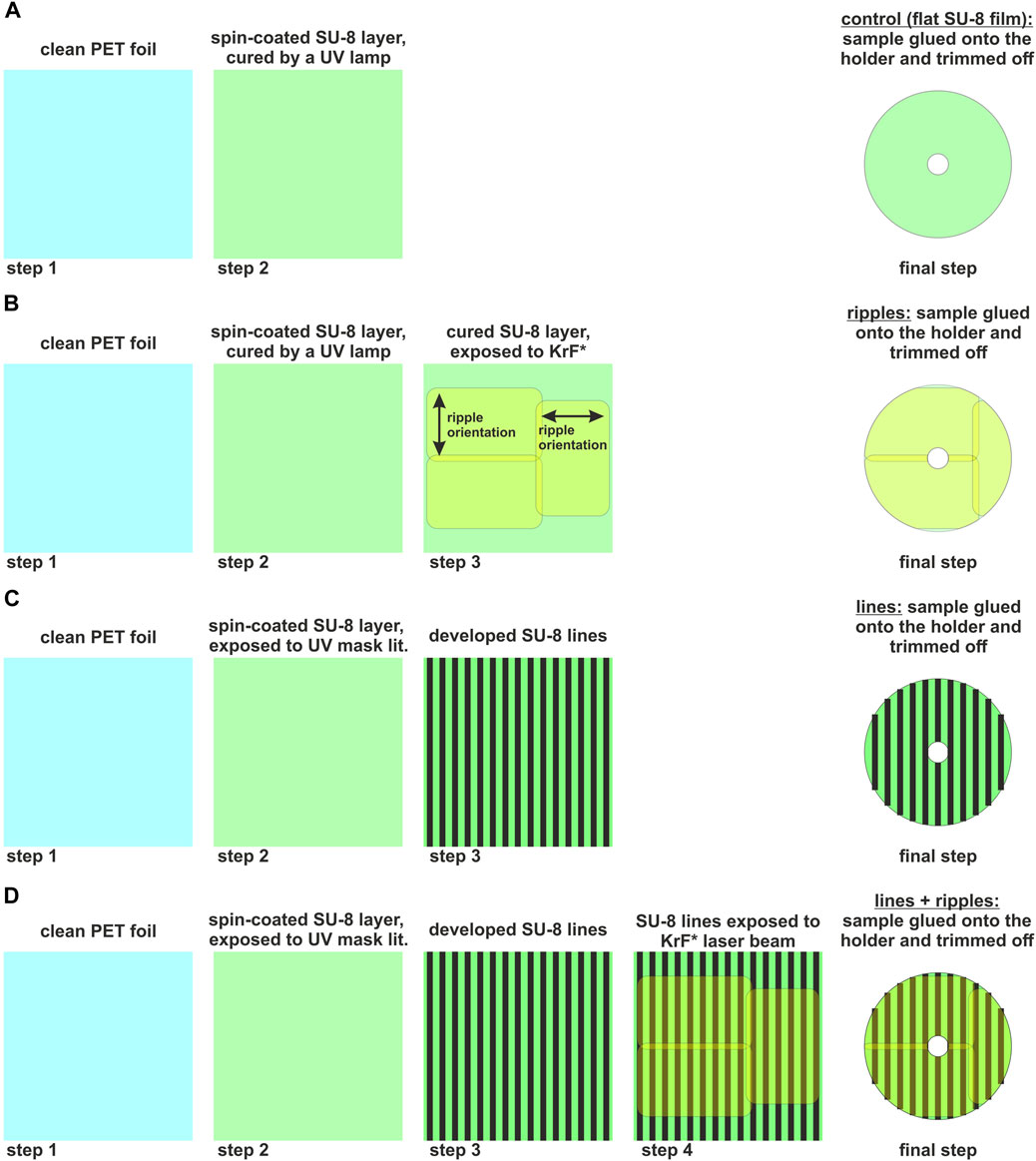
FIGURE 1. Schematics showing the main steps in sample preparation process. (A) Control sample (flat SU-8 film); (B) ripples produced by exposure to KrF* laser beam: three exposure areas were used to cover the whole sample; (C) lines produced by UV lithography: in step 3 and final, the green lines correspond to the SU-8 lines, and the black lines correspond to the valleys between two SU-8 lines; and (D) lines superimposed with ripples: in step 3, 4 and final, the green lines correspond to the SU-8 lines, and the black lines correspond to the valleys between two SU-8 lines; ripple orientation is exactly as depicted in step 3 of (B).
UV mask lithography was used to produce SU-8 lines on PET substrates. The spin-coated and pre-baked SU-8 films were left to dry overnight in a dark place, to avoid the SU-8 layer sticking to the masks when brought into contact. The masks were produced by bvm maskshop GmbH and Co. KG (Obertshausen, Germany) using a line array self-designed in CorelDRAW software (version 23.0.0.363, National Institute of Health, MD, United States). The lines were designed to be 10 µm wide with a 10 µm distance between two neighboring lines. The SU-8 film was exposed, through the mask, to a UV LED (AUV3-SQ32-0RT0K, Broadcom, Sao Polo, Brazil), with a peak wavelength at 365 nm, for 20 s. After the exposure, the samples were post-baked at 65°C for 10 min, to speed up the cross-linking. After that, the samples were allowed to rest and cool down to room temperature, and developed within some minutes. For developing, PGMEA (propylene glycol methyl ether acetate) solvent was used to remove the unexposed material. Then, the samples were rinsed with iso-propanol, and thoroughly dried with nitrogen. Figure 1C presents the preparation steps of surfaces with lines.
2.2 Laser-induced periodic surface structures (LIPSS)
To produce ripples (on flat SU-8 films or on SU-8 lines), a KrF* (krypton fluoride) excimer laser (LPX 300, Lambda Physik, 181 Göttingen, Germany) was used, with a wavelength of 248 nm, 20 ns pulse duration, and 10 Hz pulse repetition rate. The setup is described in more details in (Richter et al., 2021).
Previously reported SU-8 ripples have been produced with an average fluence of 9 mJ/cm2, by applying 3,300, 3,500, and 3,800 pulses, at incidence angles θ of 40°, 50° and 60° (Kalachyova et al., 2017). In our study, we started initially by producing ripples with 3,500 pulses, at five different incidence angles θ (0°, 10°, 20°, 30° and 40°), applying an average fluence of 10 mJ/cm2. Due to an inclined incidence angle, the laser-exposed area grows according to formula A(θ) = A(0°)/cosθ, where A(0°) is the area exposed to the laser beam at normal incidence, θ = 0°. Therefore, to keep the fluence constant over the whole range of incidence angles θ, the pulse energy was increased accordingly. Laser beam energy was measured with a high-area high-damage energy sensor (J45LP-MUV, Coherent, Portland, United States) with the help of a laser energy meter (FieldMaxII-P™, Coherent, Portland, United States). The results regarding the spatial period, height and adhesiveness to natural spider silk, for incidence angles θ of 0° and 30° were reported in (Buchberger et al., 2023).
In order to decide on what type of ripples should be used for the adhesion measurements, we studied the influence of the number of pulses on the SU-8 ripples’ average aspect ratio. We produced ripples at the same incidence angles θ (that is, 0°, 10°, 20°, 30° and 40°) using 6,000 pulses and 9,000 pulses. Samples were analyzed by FIB and SEM imaging. Based on these results, we chose to study the adhesion of the ripples produced at θ = 40° with 6,000 pulses. Furthermore, to structure a square area of 3 × 3 cm2, more laser beam exposures were performed, as shown in Figure 1B (step 3) for nanostructured surfaces, and in Figure 1D (step 4) for the lines superimposed with ripples. First, the upper left corner was exposed, then the sample was moved upwards and the lower left corner was exposed. Later, the sample was rotated 90° left-hand side, and exposed once more.
For a given average fluence and incidence angle, nanoripple formation depends on the number of pulses. As there is not much information in literature about nanoripples on SU-8, we exposed SU-8 films to the same average fluence of 10 mJ/cm2 under five incidence angles θ (0°, 10°, 20°, 30° and 40°), while varying the number of pulses from 1,500 to 3,000 pulses. This was done by exposing cured SU-8 films as shown in Figure 2. Area 1 was exposed to 1,500 pulses. Afterwards, the sample was manually moved 4–5 mm to the left, and was exposed to 500 pulses more, resulting in area 2 getting a total of 2000 pulses. Then the procedure was repeated until area 4 was exposed to a total of 3,000 pulses. Area 5 is virtually identical to area 3, both being exposed to a total of 2,500 pulses. Area 6 is virtually identical to area 2, both being exposed to a total of 2000 pulses; and area 7 is virtually identical to area 1, both being exposed to 1,500 pulses. SEM images were taken in the points marked with an “x” and spatial periods were calculated for the samples were ripples had formed. Spatial period of 2,500 pulses ripples was calculated as the average of the spatial periods calculated for areas 3 and 5; and spatial period of 3,000 pulses ripples was calculated as the average of the spatial periods calculated for the two positions imaged in area 4.
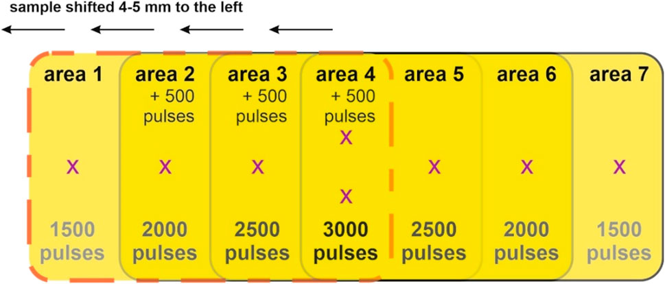
FIGURE 2. Scheme presenting the sequence of KrF* exposures used to produce ripples with 1,500 pulses, 2,000 pulses, 2,500 pulses and 3,000 pulses in a single sample, for a given incidence angle, at 10 mJ/cm2 average fluence. Pink dashed line shows the outline of the laser beam spot. Once area 1 was exposed to 1,500 pulses, the sample was manually shifted 4–5 mm towards the left, and 500 more pulses were shot onto the samples. The procedure was repeated until area 4 got a total of 3,000 pulses. This exposure scheme was repeated for all five laser beam incidence angles.
2.3 Scanning electron microscope (SEM) imaging and analysis
For SEM (model REM 1540XB-Crossbeam, Zeiss, Oberkochen, Germany) imaging, samples were sputter coated (AE1230, EMScope, Ashford, United Kingdom) for 3 min at a deposition current of 20 mA at a power of 14.3 W. This resulted in a gold layer thickness of 8–10 nm. Three SEM images were acquired per exposed area: one image on the left-hand side of the sample, one image in the center of the sample, and one image on the right-hand side of the sample. The SEM images were later analyzed by using the free software Gwyddion (version 2.61, Czech Metrology Institute, Brno, Czech Republic) to calculate the spatial period in the three analyzed areas, and to calculate the average values. The procedure is described in more detail in (Buchberger et al., 2023).
2.4 Focused ion beam (FIB) cuts and analysis
Prior to FIB cuts, samples were sputter coated (AE1230, EMScope, Ashford, United Kingdom) for 4 min at a deposition current of 20 mA at a power of 14.3 W. This resulted in a gold layer thickness of approximately 12 nm. For FIB cutting and imaging, a 1540XB-Crossbeam device (Zeiss, Oberkochen, Germany) was used, which combines a GEMINI® field-emission scanning electron microscope for imaging (FE-SEM) and a FIB tool for cutting, with a Ga⁺-filament as ion source. In the investigated region of interest, rectangles or trapezoids with sizes between 10–15 µm were cut, by using a milling current of 200–500 pA and an acceleration voltage of 30 kV. Three FIB cuts images were acquired per sample (left hand-side, center, and right hand-side) and evaluated using the free software ImageJ (version v1.54b, National Institute of Health, United States), in order to measure the average ripple height in the three investigated areas, and to calculate the average values. The procedure is described in more details in (Buchberger et al., 2023).
2.5 Electrospinning
For electrospinning and peel-off tests, each sample was fixed with double sided adhesive tape onto an aluminum sample carrier. Later on, the excess sample, that is the sides and the central part with a diameter of about 5–6 mm, were cut out (as shown in Figures 1A–D, final steps).
Electrospinning, i.e., the method of producing and depositing polymer nanofibers onto a given surface, was done using a custom-made setup, described in more details in (Lifka et al., 2023). The setup is made of a custom-made syringe pump, a 1 mL plastic syringe (Omnifix-F, B Braun SE, Melsungen, Germany), a blunt needle tip (Sterican 21G x 7/8″ blunt, B. Braun SE, Melsungen, Germany), and a high-voltage generator (HCP 35–35,000, FuG Elektronik GmbH, Schechen, Germany). The sample carrier together with the sample were fixed on an aluminum piston, with a 5 mm diameter, connected to the ground electrode of the high-voltage generator. The sample carrier and the custom-made syringe pump were fixed onto individual lab boys, which allowed adjusting their height. The setup was arranged in a horizontal configuration, to avoid polymer droplets falling onto the sample and destroying the nonwoven. The syringe blunt needle was placed horizontally opposite the sample, at a distance of about 12–13 cm. The positive electrode of the high-voltage generator was directly clamped onto the blunt needle tip by use of an alligator clamp.
For the electrospun nanofibers, 6 g of PA-6 (Nylon 6) beads were mixed with 15 g of formic acid (ROTIPURAN® ≥98%, p. a., Carl Roth GmbH + Co. KG., Karlsruhe, Germany) and 29 g of acetic acid (ROTIPURAN® 100%, p. a., Carl Roth GmbH + Co. KG., Karlsruhe, Germany) at 80°C for 1–2 h, until all the beads were dissolved. The liquid polymer was loaded into the syringe, and ejected out of the blunt needle at a flow rate of 0.16 mL/h, and a voltage of 19 kV, for 5 min, until the whole sample area was covered with a uniform layer of nanofibers (nonwoven). Electrospinning was performed under 21°C ambient temperature and 30%–40% humidity.
2.6 Peel-off force measurements
To quantify the adhesiveness of the nonwoven to a given sample, the peel-off method and setup described in (Lifka et al., 2022) were used. The electrospun sample together with its carrier was fixed into the sample holder of the setup, which was mounted on a precision scale (Kern PLS 4200-2F, KERN and SOHN GmbH, Balingen-Frommen, Germany). First, an aluminum piston was inserted through the sample carrier and the sample, until it is in contact with the nonwoven. Later on, weights were added. The exact weights were recorded from the screen of the scale, and pictures of the peeled-off cones were taken using a USB camera. The cone diameters (d) were measured from the pictures by using ImageJ software (version v1.54b, National Institute of Health, United States), and the peel-off force per unit length (p) was calculated according to the formula:
where
Four different types of polymer surfaces were produced: controls, ripples, lines, and lines superimposed with ripples. For each type of surface, four samples were tested. For a given sample, several weights were applied onto the piston in contact with the nonwoven, the diameters of the peeled-off cone were measured until the whole nonwoven was detached from the surface, and the peel-off forces were calculated for each applied weight. Within one measurement, the mean value of the peel-off force for a given surface type was calculated by averaging the peel-off forces calculated for each of the four samples.
After the peel-off force measurements for all the surface types were finished, the nonwoven was carefully removed from the sample surface, and the samples were electrospun again. In total, the measurements were repeated five times for each individual sample. The final mean values obtained for each type of surface were calculated by averaging the mean values from the five measurements. In the Supplementary Table S1 are shown the mean values calculated for each sample, and the mean values for each of the five measurements.
In an attempt to observe the influence that surface chemistry has on the peel-off force, three SU-8 samples out of each set (that is, control, ripples, lines, and lines superimposed with ripples) were cleaned of nanofibers, and gold sputter-coated. The sputter-coating was performed under the same conditions as described in the Scanning electron microscope (SEM) imaging and analysis section. Then the procedure was followed as for the polymer samples: the samples were electrospun, the peel-off force was measured, calculated and plotted.
3 Results
3.1 Laser-induced periodic surface structures (LIPSS)
In our case, nanoripples originate from the interference of the incident laser beam with the wave diffracted by the sample surface (Rebollar et al., 2015a). For a given fluence and incidence angle, nanoripples formation depends on the number of pulses and the laser repetition rate (Rebollar et al., 2015b). In Figure 3 we present SU-8 films exposed to (1A-E) 1,500 pulses, (2A-E) 2000 pulses, (3A-E) 2,500 pulses, and (4A-E) 3,000 pulses. At 1,500 pulses there are some barely perceptible ripples starting to form at θ = 0° (Figure 3 1A) and at θ = 40° (Figure 3 1E), while at incidence angles in-between (that is, θ = 10°, 20° and 30°), the SU-8 surfaces look virtually flat (Figure 3 1B–D). Ripple formation starts becoming more obvious at 2000 pulses (Figure 3 2A–E), for all the incidence angles ranging from θ = 0° to 40°. But in order to obtain well defined ripples in SU-8 with an average fluence of 10 mJ/cm2, the lowest number of pulses is about 2,500 pulses (Figure 3 3A–E).
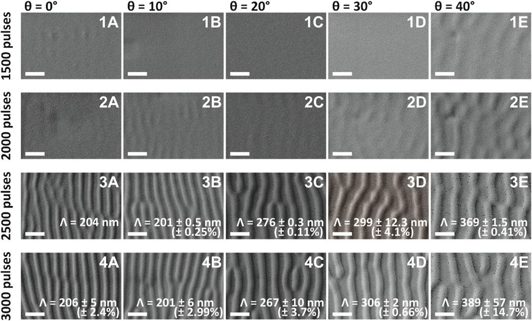
FIGURE 3. SEM images of ripples on SU-8: (1A–E) 1,500 pulses; (2A–E) 2000 pulses; (3A–E) 2,500 pulses; and (4A–E) 3,000 pulses obtained at five different incidence angles θ between the laser beam and the samples: (1A–4A) 0°; (1B–4B) 10°; (1C–4C) 20°; (1D–4D) 30°; and (1E–4E) 40°. The spatial periods Λ were possible to calculate only for ripples of 2,500 and 3,000 pulses. The spatial period for 2,500 ripples at θ = 0° was calculated only for area 3 (see Figure 2), as for area 5 the ripples were not so pronounced. The scale bar on the SEM images corresponds to 400 nm. The small black dots present in some of the images represent cracks in the sputter-coated gold layer necessary for the SEM imaging.
Usually, the spatial period Λ of ripples increases when increasing the incidence angle θ (Rebollar et al., 2015a) according to formula Λ = λ/(neff - sinθ), where λ is the wavelength of the laser beam and neff is the effective refractive index which lies between the refractive indices of air and of the polymer (in this case, SU-8). Interestingly, for the ripples produced with 2,500 pulses (Figure 3 3A, B) and 3,000 pulses (Figure 3 4A, B), the spatial periods at θ = 0° are similar to the ones produced at θ = 10°. Moreover, the spatial period for θ = 10° seems to be a couple of nm smaller than the spatial period for θ = 0°. Also, the spatial periods of ripples produced at incidence angles θ = 0°, 10°, and 20° with 2,500 pulses (Figure 3 3A–C) are similar to the ones produced with 3,000 pulses (Figure 3 4A–C), diverging substantially for θ = 30° (Figure 3 3D, 4D) and θ = 40° (Figure 3 3E, 4E).
In Figure 4 we present a comparison of ripples obtained by exposure to: 3,500 pulses, 6,000 pulses, and 9,000 pulses. As before, the average fluence was around 10 mJ/cm2 and the laser beam incidence angles θ = 0°, 10°, 20°, 30° and 40°. For each sample, three SEM images were taken at three different points (left, center and right hand-side). Spatial periods were calculated for each image, and the three values were averaged and presented in Figure 4 and Table 1.
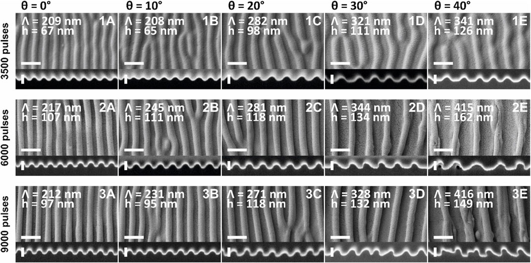
FIGURE 4. SEM and FIB cut images of ripples on SU-8: (1A–E) 3,500 pulses; (2A–E) 6,000 pulses; and (3A–E) 9,000 pulses; obtained at five different incidence angles θ between the laser beam and the samples: (A) 0°; (B) 10°; (C) 20°; (D) 30°; and (E) 40°. The spatial periods Λ and the height of the ripples h are indicated for each of the samples. The scale bar on the SEM images corresponds to 400 nm, and the scale bar on the FIB cut images corresponds to 100 nm. The small black dots in some of the images represent cracks in the sputter-coated gold layer, necessary for the SEM imaging.
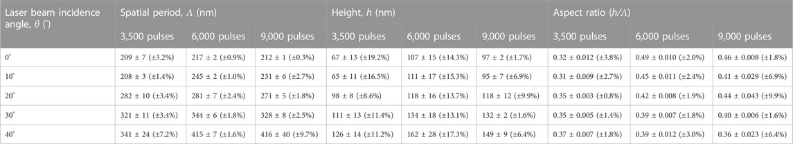
TABLE 1. Spatial period Λ, average height h, and aspect ratio (h/Λ) for ripples of 3,500 pulses, 6,000 pulses, and 9,000 pulses for the 5 different incidence angles, given as average ±standard deviation, as measured from SEM and FIB cut images.
As it was noticed for the ripples of 2,500 pulses (Figure 3 3A, B) and for the ones of 3,000 pulses (Figure 3 4A, B), there is no difference in the spatial periods of ripples produced under θ = 0° and 10° in the samples exposed to 3,500 pulses (Figure 4 1A, 1B). This is not the case for ripples of 6,000 and 9,000 pulses. Comparing the 3 sets of ripples (i.e., 3,500 pulses, 6,000 pulses, and 9,000 pulses), the overall smallest spatial periods are found in the 3,500 pulses ripples (Figure 4 1A–E), proving again that ripples spatial period increases with increasing number of pulses (Rebollar et al., 2015a). The absolute smallest spatial period of 208–209 nm was recorded for the ripples produced at 10° (Figure 4 1B) and 0° (Figure 4 1A) incidence angles, respectively. The highest spatial periods were obtained for the 6,000 pulses ripples (Figure 4 2A–E). Even though over the whole range of incidence angles from 0° to 30° the 9,000 pulses ripples have smaller spatial periods when compared to 6,000 pulses ones, the ripples produced at 40° incidence angle have the same spatial period (Figure 4 2E, 3E). The absolute standard deviations are relatively small (Table 1), ranging from 1 nm (for the sample produced at 0° with 9,000 pulses) to 40 nm (for the sample produced at 40° with 9,000 pulses), making the corresponding relative standard deviations range from 0.3% to 9.7%. The plot showing the linear dependence between the ripples spatial period and the laser beam incidence angle (for the three different number of pulses: 3,500, 6,000, and 9,000 pulses) is shown in Supplementary Figure S2.
The heights of the ripples were measured from FIB cut images, taken at three different positions on each sample (left, center and right hand-side). For each position, 15–25 ripples were evaluated, and averaged for each individual location. Later on, the three average values were again averaged and presented in Table 1 and Figure 4.
Comparing the three sets of ripples (3,500 pulses, 6,000 pulses, and 9,000 pulses), the overall shortest heights are found in the 3,500 pulses ripples (Figure 4 1A–E), with the absolute shortest heights of 65 and 67 nm being recorded for the ripples produced at 10° (Figure 4 1B) and 0° (Figure 4 1A) incidence angle, respectively. The ripples produced at 20° with 6,000 pulses (Figure 4 2C) and 9,000 pulses (Figure 4 3C) have the same average height of 118 nm, and the ripples produced at 30° with 6,000 pulses (Figure 4 2D) and 9,000 pulses (Figure 4 3D) have similar average height of 132–134 nm. The overall tallest ripples were obtained for the 6,000 pulses (Figure 4 2A–E). This means, for SU-8 ripples the height increases with increasing number of pulses, and tends to saturate around 6,000 pulses. This saturation can be explained by a balance between the involved processes of scattering, feedback, and smoothing effects (Ehrhardt et al., 2020). The absolute standard deviations are rather high (Table 1), ranging from 2 nm (for the samples produced at 0° and 30° with 9,000 pulses) to 28 nm (for the sample produced at 40° with 6,000 pulses), making the corresponding relative standard deviations range from 1.7% to 19.2%. The plot showing the linear dependence between the ripples height and the laser beam incidence angle (for the three different number of pulses: 3,500, 6,000, and 9,000 pulses) is shown in Supplementary Figure S3.
The aspect ratio of a single ripple was calculated as the ratio between the average height h and the average spatial period Λ, and is presented in Table 1. The aspect ratio of the 3,500 pulses ripples tends to increase (from 0.31–0.32 to 0.37) when increasing the laser beam incidence angle. The aspect ratio of the 6,000 pulses ripples, on the contrary, tends to decrease (from 0.49 to 0.39) when increasing the laser beam incidence angle. The aspect ratio of the 9,000 pulses ripples has generally the same tendency to decrease, with a small exception for the θ = 10° sample, with an aspect ratio of 0.41, situated between the aspect ratio of the θ = 0° and θ = 20° ripples (between 0.44 and 0.46). The plot showing the linear dependence between the ripples aspect ratio and the laser beam incidence angle (for the three different number of pulses: 3,500, 6,000, and 9,000 pulses) is shown in Supplementary Figure S4.
The final height of the ripples results from a balance between the inhomogeneous light distribution at the sample surface due to interference of the incoming light with scattered/diffracted light, or from the interaction with electromagnetic surface waves and the feedback mechanisms for ripple formation, i.e., selective material removal or swelling. Both effects can depend on the number of applied laser pulses, the specific structure geometry, or irradiation parameters, such as the angle of incidence. We see that the height increases with increasing the beam incidence angle. The reason is not clear for us yet, but similar effects have been reported in (Rebollar et al., 2014; Rebollar et al., 2015a).
3.2 Samples for electrospinning and peel-off force measurements
To quantify the adhesiveness of each type of polymer surface, nanofibers were deposited onto each sample, and then a peel-off test was used to detach the nonwoven from the sample surface. Three types of structured surfaces were produced, tested and compared to the control samples (flat SU-8 films) (Figure 5 1A): ripples (Figure 5 2A–C), lines (Figure 5 3A–C), and lines superimposed with ripples (Figure 5 4A–C).
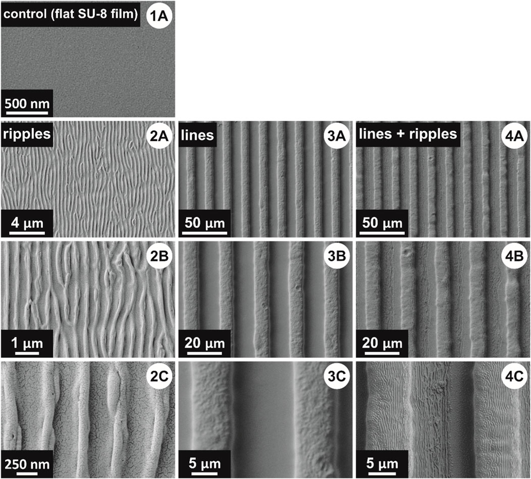
FIGURE 5. Scanning electron microscope (SEM) images of the four tested surfaces: (1A) control sample; (2A–C) ripples; (3A–C) lines; and (4A–C) lines superimposed with ripples. The small black dots in some of the images represent cracks in the sputter-coated gold layer, necessary for the SEM imaging.
In a theoretical approach, modelling the interaction of nanofibers (30 nm diameter) with a nanostructured surface, the total relative energy for the nanofibers decreases the most for spatial periods in the order of 300–350 nm, and heights in the range of 200–300 nm (Lifka et al., 2022). In our case, the artificial nanofibers have diameters ranging from 25 nm up to 175 nm (mean diameter D = 83 nm ± 32 nm, measured from SEM images, for n = 70 fibers), and as nanotopography we chose to produce ripples by exposure to 6,000 pulses of the KrF* laser beam, under an incidence angle of θ = 40° (Figure 5 2A–C). To cover a total area of 3 cm2, three laser exposure spots were used, as shown in Figure 1B (step 3), thus reducing the sample preparation time by 15 min, while offering the advantage of having the most uniform spatial period (Λ = 415 nm ± 7 nm) and the highest ripples (h = 162 ± 28 nm).
For UV lithography, the mask was designed in CorelDRAW. In the design, the lines had a width of 10 µm and the distance between two adjacent lines was 10 μm, as these were the smallest features the producing company could offer. In the real mask, the opaque areas (corresponding to the valleys in the final lines) were larger than 10 μm, which subsequently lead to the transparent areas (corresponding to the lines) being narrower. Therefore, the lines have a width of about 8–9 μm, and the distance between two adjacent lines is 11–12 μm, respectively (Figure 5 3, 4A–C). The lines could have been made wider by increasing the UV exposure time, but at the cost of the line’s height and wall sharpness, as an increased exposure time would allow the cross-linking of the material in the valleys, between the lines.
3.3 Electrospinning and peel-off tests
The peel-off force is defined as the force necessary to detach the nonwoven from the surface it adheres to. Peel-off force per unit length was measured for the control samples (flat SU-8 films), as well as for the structured samples (ripples, lines, and lines superimposed with ripples). For each of the surface type, four samples were produced and tested. For each sample, the peel-off force was measured by Eq. 1 in Peel-off force measurements section. The measurements were repeated five times for each sample, and a mean value of the peel-off force per unit length was calculated for each measurement. The results for each individual measurement are presented in the Supplementary Table S1. In measurement number 5, the measured peel-off force for sample 4 resulted in a standard deviation bigger than 55% (the peel-off force per unit length was measured to be 1.9 to 3 times bigger than for samples 1–3). As this was inconsistent with the other four measurements, we assume that it happened due to external factors, most probably due to friction between the piston and the sample holder. Therefore, we decided to not include that result into further calculations, and the mean value for that measurement was calculated as the average of the first three samples. A picture summary of the peel-off force per unit length measurements is presented in Figure 6: m is the applied weight, d is the diameter of the removed nonwoven layer, and p is the peel-off force per unit length.
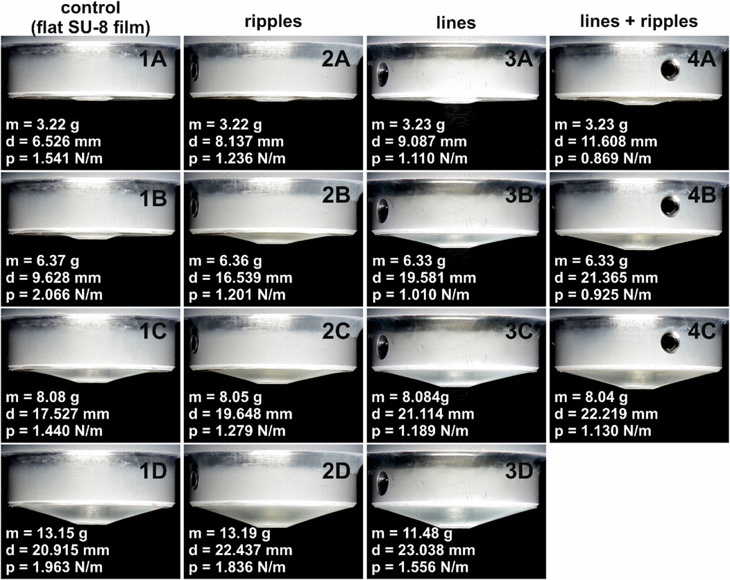
FIGURE 6. Images acquired during the peel-off force measurements: (1A–D) control sample (flat SU-8 film); (2A–D) ripples; (3A–D) lines; and (4A–C) lines superimposed with ripples, at different applied weights: (1A–4A) 3.22–3.23 g; (1B–4B) 6.33–6.37 g; (1C–4C) 8.04–8.08 g; and (1D–4D) 13.15–13.19 g for samples 1 and 2, and 11.48 g for sample 3. Note: for lines superimposed with ripples, the peel-off measurement was stopped at a weight of 8.04 g as almost the whole nonwoven was removed from the structured area. The values of m, d, and p stand for the weight, diameter, and peel-off force per unit length, respectively.
In the first row of images in Figure 6, one can easily see that even at the smallest applied weights (3.22–3.23 g), the diameter of the detached nonwoven is visibly bigger for the lines (Figure 6 3A) and lines superimposed with ripples (Figure 6 4A), compared to the control (Figure 6 1A). This means, the peel-off force necessary to remove the nonwoven from these surfaces is visibly smaller than for the control surface. When increasing the applied weights (for example, the column 1A to 1D of Figure 6), the nonwoven gradually detaches from the surface of the sample. Comparing images 1D-3D and 4C, it can be observed that to detach the same diameter of the nonwoven (d = 22–23 mm), the weight applied on the surface with lines superimposed with ripples is the smallest (m = 8.04 g) compared to the other samples, therefore, the peel-off force necessary to completely detach the nonwoven from this surface is the smallest.
The peel-off force per unit length mean values and corresponding standard deviations of the five measurements are presented in Table 2. The highest peel-off force per unit length p = 1.72 ± 0.25 N/m was measured for the control sample (flat SU-8 film). For all the structured surfaces, the measured peel-off force per unit length mean values were lower than for the control sample. The Student’s t-test (two-tailed distribution, two-sample unequal variance (heteroscedastic)) revealed that only for lines and lines superimposed with ripples, the measured mean values are significantly lower than the control: the p-values are 0.015743, and 0.00751, respectively. The lines have reduced the nanofiber adhesion force by 27.9%, and the lines superimposed with ripples–by 33.1%, when compared to the control sample. The average values are plotted and shown in Figure 7.
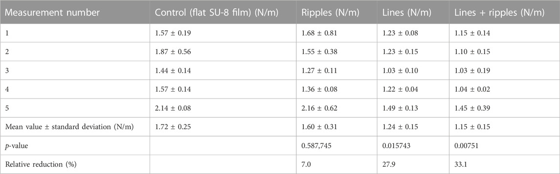
TABLE 2. Tabulated peel-off force per unit length results (average of five measurements performed on four samples of each surface type) for the SU-8 samples: control sample (flat SU-8 film); ripples; lines; and lines superimposed with ripples. Measured values of each individual measurement is shown in the Supplementary Material.
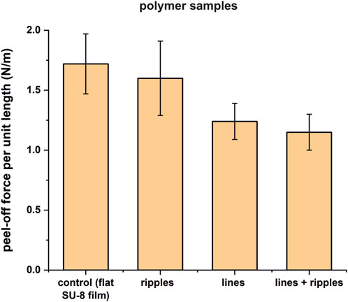
FIGURE 7. Bar plot representing the average peel-off force per unit length results for the four tested sample sets from Table 2. The peel-off force per unit length is generally lower for all the micro- and/or nanostructured samples when compared to the control sample, but only significantly lower for the lines and lines superimposed with ripples.
To observe the influence of the surface chemistry on the peel-off force, three SU-8 samples out of each set of samples were stripped of nanofibers, and gold sputter-coated. These gold sputter-coated samples were electrospun, the peel-off forces were measured, and the averaged results are shown in Table 3 and Figure 8. Generally, the peel-off forces are about 1.9–2.5 times higher than the peel-off forces measured on the polymer samples, and the standard deviations are quite small, ranging from 0.04 to 0.23 N/m. The peel-off force values for the rippled surfaces is similar to the control, which means that for this given surface material-nanofiber combination, the nanostructures do not reduce the adhesion force. A significant adhesion reduction is obtained only for the lines superimposed with ripples (Student’s t-test shows a p-value of 0.00249). But the adhesion reduction is only in the range of 15%, twice as low when compared to the polymer counterparts.
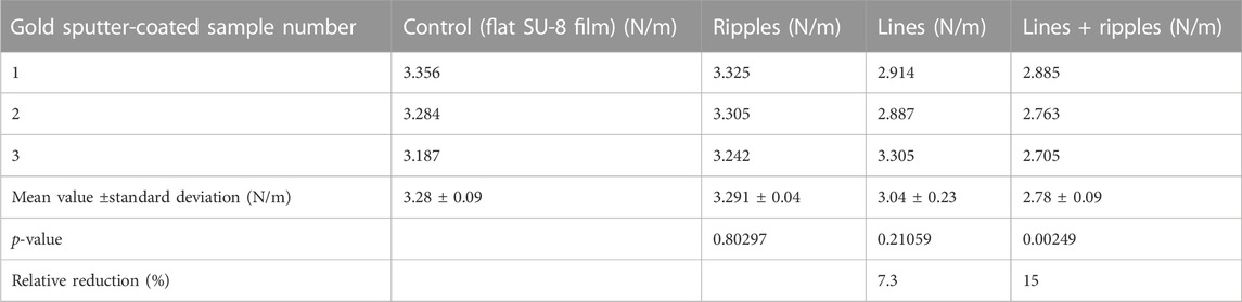
TABLE 3. Tabulated peel-off force per unit length results for the gold sputter-coated samples: control sample (flat SU-8 film) sputter-coated with gold; gold sputter-coated ripples; gold sputter-coated lines; and gold sputter-coated lines superimposed with ripples.
FIGURE 8. Bar plot representing the peel-off force per unit length measurements for the four tested sample sets from Table 3. When compared to the control sample, the peel-off force per unit length for ripples remains the same. For lines, it is not significantly lower, and for lines superimposed with ripples - significantly lower.
4 Discussion
To better understand how nanofibers interact with the micro- and nanotopographies, SEM images were taken after the nonwoven was removed from the sample surface. In Figure 9 one can see the SEM images of fibers interacting with: (1A-C) control sample (flat SU-8 film), (2A-C) ripples, and (3A-C) lines. Figure 9 1A–C presents the diameters of the thinnest and thickest nanofibers found in that given region of interest. Regardless of their diameter, the very first nanofibers that adhere to the control sample during the electrospinning process are lying flat onto the surface, having a larger area available to interact with the surface.
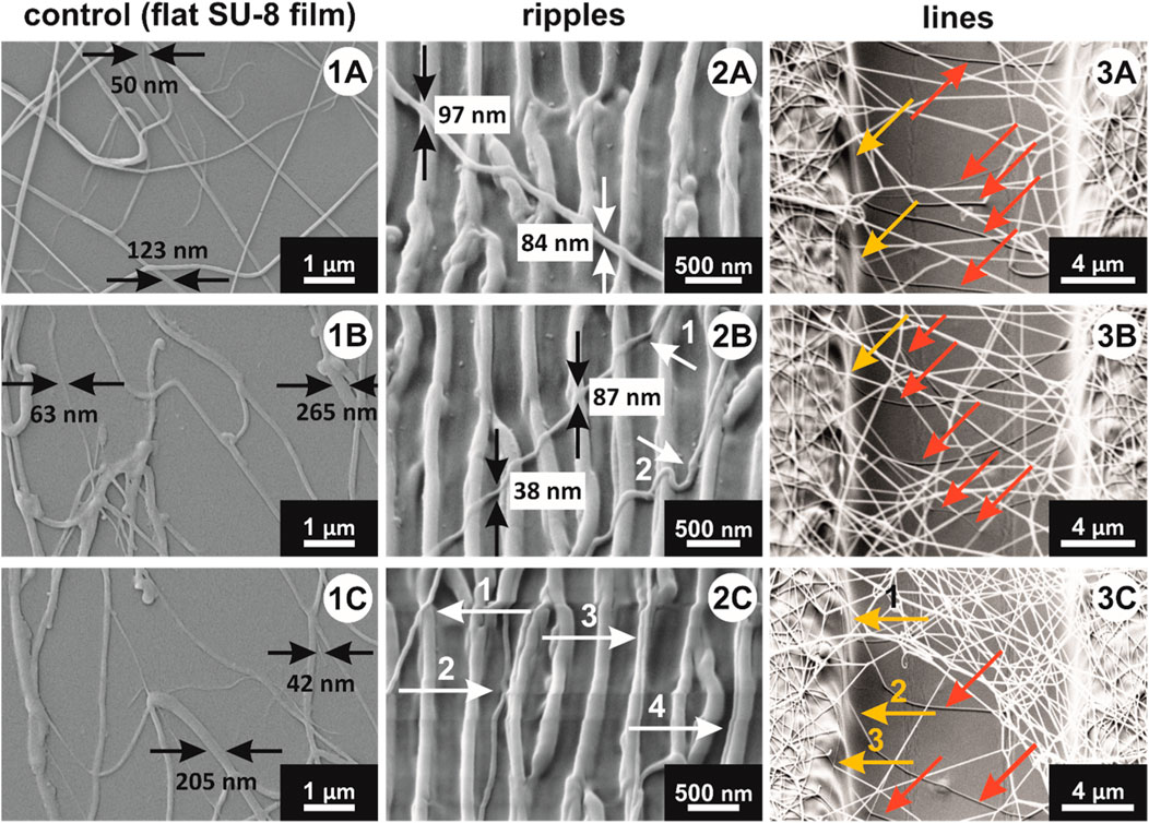
FIGURE 9. SEM images of nanofibers on: (1A–C) control sample (flat SU-8 film), showing the range of PA-6 nanofibers diameters; (2A–C) ripples, showing different nanofiber alignment relative to ripples direction; and (3A–C) lines: red arrows point to fibers on the bottom of the valleys between two lines, and yellow arrows point to fibers attached to lines’ side walls.
Figure 9 2A–C shows the way nanofibers adapt to rippled topographies. Individual nanofibers, lying almost perpendicular onto the ripples (Figure 9 2A), bridge over the valley between two nanoripples, rather than bending and adapting to the shape of the valley. Thus, the contact area between nanofibers and surface is considerably reduced. Nevertheless, the peel-off measurements results showed that the adhesion reduction is not significant. Comparing Figure 9 2A and 2B, one can notice that the bridging depends on the nanofiber diameter and/or on the distance between two given ripples. In Figure 9 2B, the upper nanofiber (arrow 1) has a smaller diameter: about 38 nm when bridging two ripples, and about 87 nm when lying flat on the top of one nanoripple. The smaller diameter allows it to bend in the valley. The diameter of the fiber pointed by the arrow 2 is visibly bigger. The nanofiber bends into the valley between the two ripples, because the distance between them is bigger compared to the other ripples on the left-hand side of it. Besides that, there are nanofibers that align parallel to the nanoripples, and Figure 9 2C shows three such nanofibers. Nanofiber 2 aligned itself on the bottom of the valley, nanofiber 3 positioned itself almost on top of the ripple, and nanofiber 4 aligned along the ripple sidewall. These fibers interact with the ripples virtually in the same way as the nanofibers adhering to the flat surfaces, in Figure 9 1A–C. Therefore, we assume that the peel-off force measured on the rippled surfaces is smaller due to the nanofibers bridging over the valleys between two ripples, but not significantly lower, because there are nanofibers that align along the valleys, tops, and sidewalls of the ripples.
Figure 9 (3A–C) show how nanofibers behave in contact with polymer lines. A similar behavior is observed as with fibers interacting with the ripples: most nanofibers bridge between two neighboring lines. Even so, several nanofibers (shown with red arrows in Figure 9 (3A–C) are bent and adhere to the valleys between the lines, meaning, there are different ways nanofibers align onto the microstructures. In Figure 9 (3A, 3B), yellow arrows point to the nanofibers that follow the geometry of the micro-pattern, attaching themselves to the top of the lines, side walls and valleys in between the lines. Similar example of interaction between nanofibers and micro-topography is shown in Figure 9 (3C), pointed to by arrow 1. Arrow 2 in the same image points to a nanofiber attached to about half of the height of the line sidewall, and then hangs free (without interacting with any surface), until it lands onto the bottom of the valley. Arrow 3 in the same image shows an example of a fiber aligned parallelly to the line. In this way, most nanofibers that are electrospun onto lines do not interact with the sample on their whole length (as the nanofibers interacting with control samples in Figure 9 (1A–C). With our electrospinning setup we obtain a single continuous nanofiber that builds up on the sample surface, until a certain thickness is reached. This means that the nanofibers interact with the structures on the sample with reduced portions of their lengths. As this leads to a reduced surface for adhesion, it also contributes to van der Waals forces reduction, and therefore to a decrease in the peel-off force.
As previously explained in Laser-induced periodic surface structures (LIPSS) section and shown in Figure 1D (step 4), the nanopatterning of lines was done by exposing three different areas of the sample. The upper and lower left sides were exposed first, by orienting the lines parallel to the polarization vector, and therefore, the lines and ripples are parallel (Figure 10 1A to D). Then the sample was rotated 90° left, and the top part of the sample was exposed. In this manner, the polarization vector is perpendicular to the lines, and therefore, the lines and the ripples are perpendicular (Figure 10 2A, D). Since the deposition of nanofibers onto the sample surface during electrospinning is random, the orientation of nanoripples should not influence the peel-off force values.
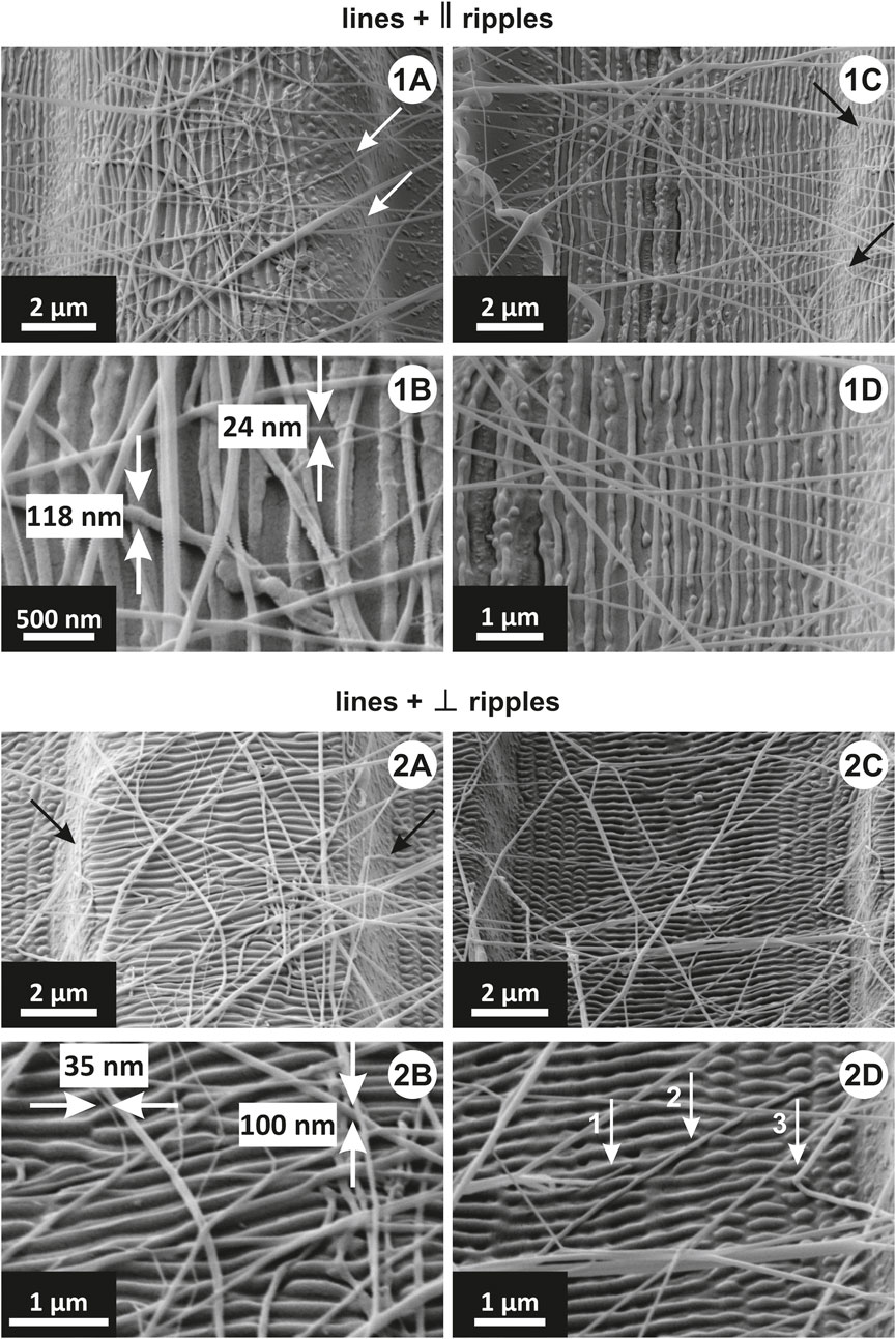
FIGURE 10. SEM images of nanofibers on: (1A–D) lines with parallel ripples and (2A–D) lines with perpendicular ripples. In (1A, 1C) white and black arrows point to fibers attached to the side walls. (1B) is a higher magnification of (1A), and shows the range of nanofibers diameters interacting with the sample. (1D) is a higher magnification of (1C). In (2A) black arrows point to fibers attached to the side walls. (2B) is a higher magnification of (2A), and shows the range of nanofibers diameters interacting with the sample. (2D) is a higher magnification of (2C), and the arrows point to the nanofibers attached to the bottom of the valleys between two lines.
In the given areas investigated by SEM, only a few nanofibers were observed to adhere to the line’s sidewalls (shown with white arrows in Figure 10 1A and with black arrows in Figure 10 1C and 2A). In Figure 10 1B and 2B, the nanofibers (with diameters ranging from 24 nm to 118 nm) are interacting with the ripples in similar manner as presented in Figure 9 2A–C: they are positioned at arbitrary angles relative to the ripple’s orientation. In Figure 10 1D, all observed nanofibers are bridging between the lines. Figure 10 2D shows a nanofiber end attached to the ripples (arrow 1), a nanofiber bridging over multiple ripples (arrow 2), and a nanofiber bridging just over two ripples (arrow 3). Interestingly, even though nanofibers orient themselves randomly on the sample surface, we have not noticed any nanofiber adhering in a parallel way to the valleys between two lines. Also, there are no nanofibers adhering to the side walls of the lines, due to geometrical limitations.
Overall, the micro- and nanotopographies in the presented samples work in the same manner: they reduce the van der Waals forces between the nanofibers and the investigated surface by reducing the surface area available for the nanofibers to adhere to. We presume that the difference in adhesion reduction comes from the structures’ cross section: ripples resemble a sine function (where the period Λ = 415 nm and the amplitude a = h/2 = 81 nm), while lines resemble a rectangular function (where the period λ = 20 µm and the amplitude a = h/2 ≈ 2.5 µm). The artificial PA-6 nanofibers produced with our electrospinning setup have an average diameter of 83 nm ± 32 nm, thus they are smaller than both the ripples and the lines. As in the electrospinning process the nanofibers are randomly positioned onto the artificial surfaces, some nanofibers align themselves parallel to the ripples, either in the valleys, on the side walls, or on top of the nanoripples. For this specific case, nanofibers interact virtually the same as with the control sample, because in this way, nanofibers attach to the ripples over long distances. The adhesion reduction in this case comes from nanofibers oriented under bigger angles relative to ripples orientation. These fibers attach themselves only to the tips of the ripples, and do not interact with valleys between two ripples, thus reducing the area of contact with the sample. In the case of lines, we have not observed any fiber that is positioned in the valley between two lines, that is, oriented parallelly to the lines. Multiple nanofibers do adhere to the bottom of the valley between two lines, but they are oriented transversally to the line’s direction. Moreover, due to geometrical consideration, there are no fibers that adhere parallelly to the side walls of lines: the sharp (90°) slope hinders parallel nanofiber adhesion. Therefore, microstructured surfaces render higher adhesion reduction (compared to nanostructured surfaces), not only due to their aspect ratio, but also due to their geometry. Even though non-significantly, ripples reduce fiber adhesion by 7%. Lines render a significantly stronger adhesion reduction of 28%. The adhesion reduction of these two types of topographies seems to be cumulative, as the lines superimposed with ripples reduce the adhesion by 33%.
5 Conclusion
Ripples on SU-8 films have been previously reported, in applications as periodic plasmonic substrates for surface enhanced Raman spectroscopy (SERS) in (Kalachyova et al., 2017; Kalachyova et al., 2019; Erzina et al., 2020). A detailed study of the laser irradiation parameters and the outcoming ripples has never been published before. In this paper, we present ripples on SU-8 films, produced under the same average fluence of 10 mJ/cm2, at five different incidence angles θ = 0°, 10°, 20°, 30° and 40°, but varying the number of pulses N = 1,500, 2,000, 2,500, 3,000, 3,500, 6,000 and 9,000. Our results show that the minimum number of pulses necessary to produce ripples on SU-8 films is around 2,500 pulses. The ripples spatial period and height increase with the number of delivered pulses, but up to a certain threshold, and we found this threshold to be at 6,000 pulses for SU-8 films. This parameter study was done in order to find the best suitable ripples for the peel-off force per unit length measurements.
Microstructures (obtained via contact lithography) nanopatterned with a partially polarized excimer laser beam have been reported before in AR-N 4340 photoresist (Ehrhardt et al., 2020). We present for the first time a combination of UV mask lithography and KrF* excimer laser beam nanostructuring in the SU-8 epoxy photoresist. The combination of these two techniques was done to replicate the hierarchical micro- and nanotopography of the U. plumipes calamistrum, and to test the adhesion of artificial nanofibers to these surfaces. Four types of surfaces were produced and tested: control samples (flat SU-8 films), ripples, lines, and lastly lines superimposed with ripples. Polyamide-6 (PA-6, Nylon) nanofibers were electrospun onto the sample, and nanofiber adhesion was measured by means of a peel-off test. The peel-off test results indicate that the microstructures have a stronger influence on the adhesion reduction than the nanostructures: ripples reduce fiber adhesion non-significantly by 7%, whereas the lines reduce it significantly, by 28%, when compared to the control samples. Nevertheless, the highest adhesion reduction of 33% is obtained for the samples combining the lines with the ripples. Also, we observed that nanofiber adhesion is strongly influenced by surface chemistry, and when comparing adhesion to polymer and to gold sputter-coated surfaces, the polymer surfaces are less adhesive for PA-6 nanofibers. Therefore, our results open new insights into the parameters (single structures aspect ratio, distance between two structures) and surface morphology (micro- or nanostructures, or both) necessary to account for whenever designing tools for nanofiber handling (spoolers, convey belts).
Data availability statement
The original contributions presented in the study are included in the article/Supplementary Material, further inquiries can be directed to the corresponding author.
Author contributions
CP: Formal Analysis, Investigation, Methodology, Writing–original draft, Writing–review and editing. SL: Methodology, Software, Writing–review and editing. GB: Funding acquisition, Project administration, Supervision, Writing–review and editing. WB: Funding acquisition, Project administration, Supervision, Writing–review and editing, Conceptualization. JH: Funding acquisition, Project administration, Supervision, Writing–review and editing, Conceptualization.
Funding
The author(s) declare financial support was received for the research, authorship, and/or publication of this article. This work was supported by the European Union’s Horizon 2020 research and innovation program through the “BioCombs4Nanofibers” project (Grant Agreement No. 862016). Part of the research was funded by the Austrian Science Fund (FWF), in the course of the “Functional Surfaces with Liquid Diode Characteristics” project (T1270-N).
Acknowledgments
We gratefully acknowledge Heidi Piglmayer-Brezina and Günter Hesser for their help in acquiring SEM and FIB cuts images, as well as Alfred Nimmervoll and Bernhard Fragner for their technical support.
Conflict of interest
The authors declare that the research was conducted in the absence of any commercial or financial relationships that could be construed as a potential conflict of interest.
Publisher’s note
All claims expressed in this article are solely those of the authors and do not necessarily represent those of their affiliated organizations, or those of the publisher, the editors and the reviewers. Any product that may be evaluated in this article, or claim that may be made by its manufacturer, is not guaranteed or endorsed by the publisher.
Supplementary material
The Supplementary Material for this article can be found online at: https://www.frontiersin.org/articles/10.3389/fmats.2023.1281992/full#supplementary-material
References
Baji, A., Zhou, L., Mai, Y.-W., Yang, Z., and Yao, H. (2015). On the Adhesion performance of a single electrospun fiber. Appl. Phys. A 118, 51–56. doi:10.1007/s00339-014-8865-6
Bayrak, E. (2022). “Nanofibers: production, characterization, and tissue engineering applications,” in 21st century nanostructured materials - physics, chemistry, classification, and emerging applications in industry, biomedicine, and agriculture. Editor P. V. Pham China, (IntechOpen). doi:10.5772/intechopen.102787
B. Bhushan (Editor) (2012). Encyclopedia of nanotechnology (Dordrecht: Springer Netherlands). doi:10.1007/978-90-481-9751-4
Buchberger, G., Meyer, M., Plamadeala, C., Weissbach, M., Hesser, G., Baumgartner, W., et al. (2023). Robustness of antiadhesion between nanofibers and surfaces covered with nanoripples of varying spatial period. Front. Ecol. Evol. 11. doi:10.3389/fevo.2023.1149051
Çallioğlu, F. C., and Güler, H. K. (2019). “7. Natural nanofibers and applications,” in Green electrospinning. Editors N. Horzum, M. M. Demir, R. Muñoz-Espí, and D. Crespy (De Gruyter), USA, 157–188. doi:10.1515/9783110581393-007
Chapman, R. A. (2010). Applications of nonwovens in technical textiles. 1st edition. Amsterdam, The Netherlands: Elsevier.
Chen, Z., and Lee, J.-B. (2021). Biocompatibility of SU-8 and its biomedical device applications. Micromachines 12, 794. doi:10.3390/mi12070794
Ehrhardt, M., Lai, S., Lorenz, P., and Zimmer, K. (2020). Guiding of LIPSS formation by excimer laser irradiation of pre-patterned polymer films for tailored hierarchical structures. Appl. Surf. Sci. 506, 144785. doi:10.1016/j.apsusc.2019.144785
Erzina, M., Trelin, A., Guselnikova, O., Dvorankova, B., Strnadova, K., Perminova, A., et al. (2020). Precise cancer detection via the combination of functionalized SERS surfaces and convolutional neural network with independent inputs. Sensors Actuators B Chem. 308, 127660. doi:10.1016/j.snb.2020.127660
Farhaj, S., Conway, B. R., and Ghori, M. U. (2023). Nanofibres in drug delivery applications. Fibers 11, 21. doi:10.3390/fib11020021
Ghajarieh, A., Habibi, S., and Talebian, A. (2021). Biomedical applications of nanofibers. Russ. J. Appl. Chem. 94, 847–872. doi:10.1134/S1070427221070016
João, C. F. C., Baptista, A. C., Ferreira, I. M. M., Silva, J. C., and Borges, J. P. (2016). “Natural nanofibres for composite applications,” in Fibrous and textile Materials for composite applications textile science and clothing Technology. Editors S. Rana, and R. Fangueiro (Singapore: Springer Singapore), 261–299. doi:10.1007/978-981-10-0234-2_8
Joel, A.-C., Meyer, M., Heitz, J., Heiss, A., Park, D., Adamova, H., et al. (2020). Biomimetic combs as antiadhesive tools to manipulate nanofibers. ACS Appl. Nano Mat. 3, 3395–3401. doi:10.1021/acsanm.0c00130
Joel, A.-C., Rawal, A., Yao, Y., Jenner, A., Ariotti, N., Weissbach, M., et al. (2023). Physico-chemical properties of functionally adhesive spider silk nanofibres. Biomater. Sci. 11, 2139–2150. doi:10.1039/D2BM01599D
Joel, A.-C., Scholz, I., Orth, L., Kappel, P., and Baumgartner, W. (2016). Morphological adaptation of the calamistrum to the cribellate spinning process in Deinopoidae (Uloboridae, Deinopidae). R. Soc. open Sci. 3, 150617. doi:10.1098/rsos.150617
Kailasa, S., Reddy, M. S. B., Maurya, M. R., Rani, B. G., Rao, K. V., and Sadasivuni, K. K. (2021). Electrospun nanofibers: materials, synthesis parameters, and their role in sensing applications. Macromol. Mat. Eng. 306, 2100410. doi:10.1002/mame.202100410
Kalachyova, Y., Mares, D., Jerabek, V., Elashnikov, R., Švorčík, V., and Lyutakov, O. (2019). Longtime stability of silver-based SERS substrate in the environment and (bio)environment with variable temperature and humidity. Sensors Actuators A Phys. 285, 566–572. doi:10.1016/j.sna.2018.11.037
Kalachyova, Y., Mares, D., Jerabek, V., Ulbrich, P., Lapcak, L., Svorcik, V., et al. (2017). Ultrasensitive and reproducible SERS platform of coupled Ag grating with multibranched Au nanoparticles. Phys. Chem. Chem. Phys. 19, 14761–14769. doi:10.1039/C7CP01828B
Kannan, B., Cha, H., and Hosie, I. C. (2016). “Electrospinning—commercial applications, challenges and opportunities,” in Nano-size polymers. Editor S. Fakirov (Cham: Springer International Publishing), 309–342. doi:10.1007/978-3-319-39715-3_11
Keshvardoostchokami, M., Majidi, S. S., Huo, P., Ramachandran, R., Chen, M., and Liu, B. (2020). Electrospun nanofibers of natural and synthetic polymers as artificial extracellular matrix for tissue engineering. Nanomaterials 11, 21. doi:10.3390/nano11010021
Kono, N., Nakamura, H., Mori, M., Tomita, M., and Arakawa, K. (2020). Spidroin profiling of cribellate spiders provides insight into the evolution of spider prey capture strategies. Sci. Rep. 10, 15721. doi:10.1038/s41598-020-72888-6
Lifka, S., Harsányi, K., Baumgartner, E., Pichler, L., Baiko, D., Wasmuth, K., et al. (2022). Laser-processed antiadhesive bionic combs for handling nanofibers inspired by nanostructures on the legs of cribellate spiders. Beilstein J. Nanotechnol. 13, 1268–1283. doi:10.3762/bjnano.13.105
Lifka, S., Stecher, C., Meyer, M., Joel, A.-C., Heitz, J., and Baumgartner, W. (2023). Biomimetic, antiadhesive surface structure inspired by the calamistra setae of cribellate spiders for electrospun nanofiber handling. Front. Ecol. Evol. 11, 1099355. doi:10.3389/fevo.2023.1099355
Lu, T., Cui, J., Qu, Q., Wang, Y., Zhang, J., Xiong, R., et al. (2021). Multistructured electrospun nanofibers for air filtration: a review. ACS Appl. Mat. Interfaces 13, 23293–23313. doi:10.1021/acsami.1c06520
Meyer, M., Buchberger, G., Heitz, J., Baiko, D., and Joel, A.-C. (2021). Ambient climate influences anti-adhesion between biomimetic structured foil and nanofibers. Nanomaterials 11, 3222. doi:10.3390/nano11123222
Nisticò, R. (2020). Polyethylene terephthalate (PET) in the packaging industry. Polym. Test. 90, 106707. doi:10.1016/j.polymertesting.2020.106707
Rebollar, E., Castillejo, M., and Ezquerra, T. A. (2015a). Laser induced periodic surface structures on polymer films: from fundamentals to applications. Eur. Polym. J. 73, 162–174. doi:10.1016/j.eurpolymj.2015.10.012
Rebollar, E., Pérez, S., Hernández, M., Domingo, C., Martín, M., Ezquerra, T. A., et al. (2014). Physicochemical modifications accompanying UV laser induced surface structures on poly(ethylene terephthalate) and their effect on adhesion of mesenchymal cells. Phys. Chem. Chem. Phys. 16, 17551. doi:10.1039/C4CP02434F
Rebollar, E., Rueda, D. R., Martín-Fabiani, I., Rodríguez-Rodríguez, Á., García-Gutiérrez, M.-C., Portale, G., et al. (2015b). In situ monitoring of laser-induced periodic surface structures formation on polymer films by grazing incidence small-angle X-ray scattering. Langmuir 31, 3973–3981. doi:10.1021/acs.langmuir.5b00285
Richter, A. M., Buchberger, G., Stifter, D., Duchoslav, J., Hertwig, A., Bonse, J., et al. (2021). Spatial Period of laser-induced surface nanoripples on PET determines Escherichia coli repellence. Nanomaterials 11, 3000. doi:10.3390/nano11113000
Roslan, N. S. A., Abdul Hamid, N., Md Isa, M. H., Muhammad, N., Mansor, M. R., and Abdul Munajat, N. (2018). Nylon electrospun nanofibre water filtration media for wastewater treatment. Mat. Res. Express 5, 105010. doi:10.1088/2053-1591/aada94
Shi, Q., Wan, K.-T., Wong, S.-C., Chen, P., and Blackledge, T. A. (2010). Do electrospun polymer fibers stick? Langmuir 26, 14188–14193. doi:10.1021/la1022328
Tian, J., Deng, H., Huang, M., Liu, R., Yi, Y., and Dong, X. (2019). “Electrospun nanofibers for food and food packaging Technology,” in Electrospinning: nanofabrication and applications (Germany: Elsevier), 455–516. doi:10.1016/B978-0-323-51270-1.00015-7
Xue, J., Xie, J., Liu, W., and Xia, Y. (2017). Electrospun nanofibers: new concepts, materials, and applications. Acc. Chem. Res. 50, 1976–1987. doi:10.1021/acs.accounts.7b00218
Keywords: bio-inspired, SU-8, UV lithography, ripples, polymer micro-and nanostructures, electrospinning, artificial nanofibers, adhesion reduction
Citation: Plamadeala C, Lifka S, Buchberger G, Baumgartner W and Heitz J (2023) Bio-inspired hierarchical polymer micro- and nanostructures for anti-adhesion applications. Front. Mater. 10:1281992. doi: 10.3389/fmats.2023.1281992
Received: 23 August 2023; Accepted: 08 November 2023;
Published: 22 November 2023.
Edited by:
Senbo Xiao, Norwegian University of Science and Technology, NorwayReviewed by:
Mari-Cruz Garcia-Gutierrez, Spanish National Research Council (CSIC), SpainKailu Xiao, Texas A&M University, United States
Esther Rebollar, Spanish National Research Council, Spain
Copyright © 2023 Plamadeala, Lifka, Buchberger, Baumgartner and Heitz. This is an open-access article distributed under the terms of the Creative Commons Attribution License (CC BY). The use, distribution or reproduction in other forums is permitted, provided the original author(s) and the copyright owner(s) are credited and that the original publication in this journal is cited, in accordance with accepted academic practice. No use, distribution or reproduction is permitted which does not comply with these terms.
*Correspondence: Cristina Plamadeala, Y3Jpc3RpbmEucGxhbWFkZWFsYUBqa3UuYXQ=