 Enbo Zhu
 Zhengwei Zhang
 Chen Wang
- 1Department of Medicine, Division of Cardiology, David Geffen School of Medicine, UCLA, Los Angeles, CA, United States
- 2Department of Medicine, Greater Los Angeles VA Healthcare System, Los Angeles, CA, United States
- 3Hunan Key Laboratory of Nanophotonics and Devices, School of Physics and Electronics, Central South University, Changsha, Hunan, China
- 4State Key Laboratory of New Ceramics and Fine Processing, Key Laboratory of Advanced Materials of Ministry of Education, School of Materials Science and Engineering, Beijing Advanced Innovation Center for Integrated Circuits, Tsinghua University, Beijing, China
Editorial on the Research Topic
Emerging chip materials and devices for post Moore’s era
Introduction
The slowdown of equivalent scaling and the end of classical Moore’s Law have brought about significant challenges for silicon-based CMOS integrated circuits. This has spurred the urgent need for the development of novel materials, device structures, integration processes, and specialized system architectures for the post Moore’s era. Inspired by More Moore, More than Moore and Beyond CMOS strategies (Ref 1: https://irds.ieee.org/), next-generation ICs demand performance improvements in various areas, including non-silicon semiconductors, beyond CMOS devices, high-density integration processes, and unique system architectures and emerging applications. Concurrently, advances in layered semiconductors, lateral epitaxial heterojunctions, integrated biochips have been propelled by the development of superior devices, enabling more energy-efficient and high speed signal processing, storage, detection, communications and system function (Figure 1).
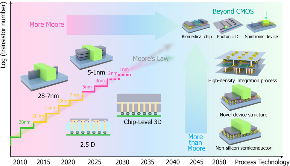
FIGURE 1. Non-silicon semiconductor, novel devices and high density integration processes powering up the post Moore’s era.
This Research Topic serves as a forum for researchers to present the state-of-the-art progress and review recent developments, challenges, and opportunities in materials, structure, devices, integration, and system to light up the post Moore’s era. This includes optimized silicon based materials, emerging layered semiconductors (Wang et al., 2018; Xie et al., 2018), next-generation interconnect materials, novel device structures (Duan et al., 2014; Li et al., 2015), new working principle devices (Liu et al., 2021; Zhang et al., 2022a), 3D integration processes (Zhang et al., 2022b; Zhang et al., 2022c), and recent progress in bioelectronics (Wang et al., 2022) and sensor technologies (Abiri et al., 2022), underlining the need for ongoing research and innovation in this field.
For the optimized silicon based materials, Islam et al. presented a simple and environmentally friendly method for low-cost production of silicon thin films on quartz substrates using aluminothermic reduction. This innovative approach addresses the long-standing challenge of obtaining high-quality silicon films using cost-effective and sustainable methods. The researchers utilized aluminothermic reduction, converting the surface of the quartz substrate in contact with an aluminum (Al) layer into elemental Si during high-temperature annealing. This research has potential applications in energy devices, electronics, Si on insulators, Si/SiO2 superlattice, and photonic crystals. The findings of this study pave the way for further investigations into the optimization of aluminothermic reduction parameters, such as the initial Al content and reduction temperature, to achieve even higher-quality Si films.
Another view from Zhang et al. addressing the challenges of synthesizing 2D lateral heterojunctions by reporting he successful growth of sub-2 nm WS2 quantum well arrays within monolayer WSe2. No double similar quantum well superlattice structures could be formed in diverse lateral heterojunctions, offering a rich array of photonic electronic properties and opening new avenues for studying topological insulators and superconductors in 2D quantum materials and devices. The innovative approach to synthesizing quantum well superlattices demonstrates the potential of these structures for a variety of applications, including advanced optoelectronics, sensors, and quantum computing.
Another milestone review from Chen et al. is focusing on electrical impedance-based sensors, specifically electrochemical impedance spectroscopy (EIS) and electrical impedance tomography (EIT), which have been explored for clinical applications over the past few decades. These applications include detecting cardiac output, pulmonary function, atherosclerotic plaques, and fatty liver disease. A critical aspect of these applications is the electrochemical properties of the interface electrodes, which determine the signal-to-noise ratio and sensitivity of measurements in biological environments. Carbon-based nanomaterials become potential candidates for enhancing the conductive properties of bioimpedance sensor electrodes. It discusses the strengths of various nanomaterials in optimizing charge transfer and measurement sensitivity. Recent advancements in wearable and implantable bioelectronics are also examined, alongside current biomedical applications of EIS and EIT. Moreover, the review identifies unmet clinical needs, such as adapting to different hemodynamic conditions and blood vessel geometries, that can be addressed by novel biomaterials for future EIS-based sensors. Despite the limiting effects of the post-Moore’s era on the development of conductive nanomaterials, further research and commercialization efforts are necessary to ensure that these novel materials meet regulatory requirements and become viable for clinical use.
Last but not least, efficient and environmentally friendly metal material machining processes are crucial in modern manufacturing. In the study from Li et al. a process condition-oriented method is proposed for predicting resource environment load data, which is essential for assessing and enhancing the environmental performance of metal material machining processes. The method introduces process conditions that comprehensively describe various aspects of the machining process, including process type, materials, processing mode, equipment, and process parameters. A resource environment load database is constructed based on these process conditions. By using limited sample data, a process condition similarity matching method based on weighted Euclidean distance is employed for predicting resource environment load data under new process conditions. The proposed method demonstrates an average prediction accuracy exceeding 90%, with environmental performance predictions using the predicted data achieving over 93% accuracy. Future research in this area may explore the impact of data set size on prediction results and compare the proposed method with alternative data-driven approaches. The development of more accurate prediction methods and the incorporation of additional factors, such as energy consumption and waste generation, could further enhance the environmental performance of metal material machining processes.
Conclusion
The Research Topic of studies in this Research Topic showcases the latest advances in novel materials and devices, addressing the few of most key challenges faced in the post-Moore’s era. As the scaling of silicon-based CMOS integrated circuits slows down, researchers are exploring alternative materials, structures, and architectures to meet the performance requirements of next-generation ICs. The studies presented here offer promising solutions to these challenges by developing innovative methods, such as aluminothermic reduction for silicon layer formation and dislocation-driven growth of quantum well superlattices. Furthermore, the research focuses on enhancing bioelectronics, such as sensors and actuators, which have far-reaching applications in disease diagnosis and the interface between organisms and devices. The development of novel nanomaterials for use in electrochemical impedance spectroscopy exemplifies the potential of these materials in biomedical applications. While the post-Moore’s era poses significant challenges, this Research Topic demonstrates that progress is being made in the development of emerging materials, devices, and architectures that can address these challenges and pave the way for a new era of innovation.
Author contributions
CW, EZ, and ZZ co-conceived this special issue as well as drafted and finalized this Editorial. All authors contributed to the article and approved the submitted version.
Funding
CW financially supported by the National Key Research and Development Program of China (2021YFA1200800), the National Natural Science Foundation of China (62004114 and 62174098), Tsinghua University Initiative Scientific Research Center, Beijing Municipal Science and Technology Commission (Z211100002421012) and Beijing Advanced Innovation Center.
Conflict of interest
The authors declare that the research was conducted in the absence of any commercial or financial relationships that could be construed as a potential conflict of interest.
Publisher’s note
All claims expressed in this article are solely those of the authors and do not necessarily represent those of their affiliated organizations, or those of the publisher, the editors and the reviewers. Any product that may be evaluated in this article, or claim that may be made by its manufacturer, is not guaranteed or endorsed by the publisher.
References
Abiri, P., Luo, Y., Huang, Z.-Y., Cui, Q., Duarte-Vogel, S., Roustaei, M., et al. (2022). 3-Dimensional electrical impedance spectroscopy for in situ endoluminal mapping of metabolically active plaques. Sensors Actuators B Chem. 354, 131152. doi:10.1016/j.snb.2021.131152
Duan, X., Wang, C., Shaw, J. C., Cheng, R., Chen, Y., Li, H., et al. (2014). Lateral epitaxial growth of two-dimensional layered semiconductor heterojunctions. Nat. Nanotechnol. 9, 1024–1030. doi:10.1038/nnano.2014.222
Li, M.-Y., Shi, Y., Cheng, C.-C., Lu, L.-S., Lin, Y.-C., Tang, H.-L., et al. (2015). Epitaxial growth of a monolayer WSe 2 -MoS 2 lateral p-n junction with an atomically sharp interface. Science 349, 524–528. doi:10.1126/science.aab4097
Liu, Y., Duan, X., Shin, H.-J., Park, S., Huang, Y., and Duan, X. (2021). Promises and prospects of two-dimensional transistors. Nature 591, 43–53. doi:10.1038/s41586-021-03339-z
Wang, C., He, Q., Halim, U., Liu, Y., Zhu, E., Lin, Z., et al. (2018). Monolayer atomic crystal molecular superlattices. Nature 555, 231–236. doi:10.1038/nature25774
Xie, S., Tu, L., Han, Y., Huang, L., Kang, K., Lao, K. U., et al. (2018). Coherent, atomically thin transition-metal dichalcogenide superlattices with engineered strain. Science 359, 1131–1136. doi:10.1126/science.aao5360
Zhang, S., Deng, X., Wang, Y., Wu, Y., Ke, S., Li, L., et al. (2022). China semiconductor Technology international conference. China: CSTIC.
Zhang, S., Deng, X., Wu, Y., Wang, Y., Ke, S., Zhang, S., et al. (2022). Lateral layered semiconductor multijunctions for novel electronic devices. Chem. Soc. Rev. 51, 4000–4022. doi:10.1039/d1cs01092a
Keywords: layered semiconductors, lateral epitaxial heterojunctions, integrated biochips, 3D integration, sensor, interconnect materials, novel device, bioelectronics
Citation: Zhu E, Zhang Z and Wang C (2023) Editorial: Emerging chip materials and devices for post Moore’s era. Front. Mater. 10:1224537. doi: 10.3389/fmats.2023.1224537
Received: 17 May 2023; Accepted: 31 May 2023;
Published: 13 June 2023.
Edited and reviewed by:
Peide Ye, Purdue University, United StatesCopyright © 2023 Zhu, Zhang and Wang. This is an open-access article distributed under the terms of the Creative Commons Attribution License (CC BY). The use, distribution or reproduction in other forums is permitted, provided the original author(s) and the copyright owner(s) are credited and that the original publication in this journal is cited, in accordance with accepted academic practice. No use, distribution or reproduction is permitted which does not comply with these terms.
*Correspondence: Chen Wang, Y2hlbndhbmcwMTAxQHRzaW5naHVhLmVkdS5jbg==