- 1Faculty of Science and Natural Resources, Universiti Malaysia Sabah, Kota Kinabalu, Sabah, Malaysia
- 2School of Materials Science and Engineering, Sichuan University of Science and Engineering, Zigong, China
- 3Material Corrosion and Protection Key Laboratory of Sichuan Province, Sichuan University of Science and Engineering, Zigong, China
- 4State Key Laboratory for Mechanical Behavior of Materials, Xi’an Jiaotong University, Xi’an, China
The crystal orientation of ceramic substrates is an important factor affecting the interface structure of metal/ceramic composite materials. However, there is little information about the interface composed of metal films and ceramic substrates with a high-index plane. In this work, we predicted the interface structure between a Nb film and a MgO(112) substrate by calculating the interface separation works of different interface models by using the first-principles calculation method. The results showed that the preferred growth direction is Nb [120], and that the value of the interface separation work is 0.35 eV/Å2. The lattice mismatch between the film and substrate is less than 3%, implying that a coherent interface type is highly realizable in Nb/MgO(112). Furthermore, we analyzed the interface structures of Nb/MgO(100), Nb/MgO(110), Nb/MgO(111), and Nb/MgO(112) and found that the unique atomic configuration of the MgO substrate is the main factor determining the preferred interface structure of Nb/MgO.
1 Introduction
The composite material formed by a metal thin film and ceramic substrate (metal/ceramic) is widely used in many important areas, such as coating, sensors, catalysis, and microelectronic devices (Ernst, 1995; Yuan et al., 2021). It is well known that the interface plays an important role in composite materials, especially when the characteristic size of the material is at the nanometer scale (Lu et al., 2009; Chen et al., 2021). Early works found that the same material deposited on the same substrate but with different substrate orientations could provide different interface structures and properties, which is called the substrate-orientation dependence of structures and properties (Shikada et al., 2009; Wang et al., 2018). For example, the growth directions of FeCo thin films which are prepared on MgO substrates are [100], [112], and [111] when the terminated planes of the substrates are (100), (110), and (111). The magnetic properties of the three FeCo films are different because of different crystalline behaviors (Shikada et al., 2009). Thus, it is important to evaluate the influence of the substrate orientation on the interface structure of metal/ceramic composite materials.
Substrate orientation is commonly expressed by a set of Miller indices [h k l], and the terminated plane is called the high-index plane, with at least one index greater than unity (Quan et al, 2013). Early works showed that some high-index planes could have stable structures, which were even more energetically stable than low-index planes after relaxation (Baski et al, 1995). More importantly, composite materials with high-index planes sometimes showed novel structures and properties that attracted great attention from researchers in recent years (Schonherr et al., 2001; Hocker et al., 2015; Han et al., 2020). For example, Han et al. (2020) recently reported a unique TiAl(111)/Ti2AlN(103) interface that can nucleate and annihilate dislocations simultaneously, and the reason for the special properties is that the interface bonding characteristics are multiple and inhomogeneous depending on local atomic configurations. Due to the progress in cutting and polishing technology, single-crystal materials with high-index terminated planes can be prepared in a single-crystal material manufacturing factory. It is possible to use the high-index planes as substrates to deposit metal films. Since any crystal plane with a stable structure could be used as the terminated plane to deposit metal films, a huge number of high-index planes and their specific atomic configurations provide a broad space for the interface design of metal/ceramic composite materials.
Single-crystal MgO is widely used as a substrate material because it has a simple sodium chloride structure and clean surfaces are easy to obtain. In experiments, there is a cubic-on-cubic orientation relationship between FCC metals and MgO substrates, and a square network of edge-type dislocation could be found along the interface (Lairson et al., 1992; Ernst, 1995). For BCC metals, the growth directions are usually [100], [112], and [110] on MgO(100), MgO(110), and MgO(111) substrates, and the interface type is semi-coherent (Shikada et al., 2009). Although the epitaxial growth of thin metal films on MgO substrates with low-index planes has been extensively studied before, the interface details of metal/MgO with high-index planes are barely known. In theory, the preferred interface structure is primarily attributed to a system’s attempt at reducing the nucleation barrier by forming low-energy interfaces. Based on this, Fu et al. (2014) studied the interface structures of Nb/MgO(100) and Nb/MgO(111) both experimentally and using first-principles calculations. The results showed that the interface structures observed in experiments have the largest interface separation work, and similar conclusions were drawn for Nb/MgO(110) (Fang et al, 2016), Nb/Al2O3(110) (Du et al., 2016), Fe/MgO(100), and V/MgO(100) (Du et al., 2017) systems. Thus, calculating the interface separation work allows us to predict the preferred interface structure.
Compared with other high-index planes, such as MgO(120) and MgO(122), the crystal structure of MgO(112) is relatively simple, which makes it a suitable case to study the high-index planes of MgO substrates. At the same time, due to the progress in cutting technology, ordinary substrate suppliers could provide single-crystal substrates with specific crystal orientations according to customer requirements. In the present work, we predicted the interface structure between a Nb thin film and a MgO(112) substrate by calculating the interface energy of different interface models. Furthermore, we compared Nb/MgO(112) with Nb/MgO(100), Nb/MgO(110), and Nb/MgO(111) and discussed the formation mechanism of the preferred Nb/MgO interface. This work not only offers details about the Nb/MgO(112) interface structure but also provides new ideas on how to obtain metal films with desired orientations.
2 Calculation model and parameters
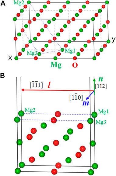
Figure 1A shows the crystal structure of a 2 × 2 × 1 MgO supercell with the indication of a MgO(112) crystal plane. Figure 1B gives the unit cell of MgO(112) with a slab model, which contains seven layers of MgO(112) and a vacuum slab. In the figure, the crystal orientation along l (Mg1–Mg2), m (Mg1–Mg3), and n directions is MgO [

FIGURE 1. (A) Crystal structure of a 2 × 2 × 1 MgO supercell. (B) Crystal structure of a MgO(112) unit cell with a slab model.
The mean absolute strain ε ((|ε11|+|ε22|+|ε12|)/3) is used to represent the average strain along the interface in the film. The slab model is built by placing six layers of Nb on the top of six layers of MgO(112) with a vacuum layer. Usually, we get a large number of coherent interface models that are constructed using two surfaces. In step 3, we narrow down the number of interface models by setting a cut-off value for the atomic number (<100) and mean absolute strain ε (<8.5%). As a result, there are four Nb(100)/MgO(112) interface models that satisfy the limit conditions. By repeating this process, we get five Nb(110)/MgO(112) interface models, nine Nb(111)/MgO(112) interface models, five Nb(120)/MgO(112) interface models, and four Nb(112)/MgO(112) interface models. In total, we get 27 Nb/MgO(112) interface models.
Interface separation work (Wsep) is defined as the work needed to separate an interface to form two surfaces (Finnis, 1996). It is written as
where ENb and EMgO are the total energies of Nb and MgO slabs, respectively. Interface distance x, defined as the nearest distance between the film and substrate, can be obtained by minimizing the total energy of the whole system with other fixed parameters. ENb/MgO is the total energy of the whole system after optimizing the interface distance, and S is the area of the interface. For each calculation model, first, we get the correct interface distance using the calculation system, with total energy as a function of the interface distance, and then, we calculate the energies of Nb and MgO slabs. Finally, we determine the interface separation works for all calculation models and use them to identify the preferred interface. Wsep is used to characterize the interface bonding strength, and the larger the value of Wsep, the more stable the interface. The electron density difference is calculated to illustrate how electrons transform along the interface (Fu et al., 2014). The electron density difference is expressed as
where ρNb/MgO is the electron density of the whole interface model; ρNb and ρMgO are the electron densities of Nb and MgO slabs, respectively. All calculations were carried out using the DFT (density functional theory) calculation engine in ATK software. A SZP (Single-Zeta plus Polarization) basis set was used to represent the distribution of valence electrons for all atoms; GGA (Generalized Gradient Approximation) was utilized to treat the exchange-correlation energy. In the total energy calculation, the cut-off energy and Monkhorst–Pack k-mesh were set at 75 Hartree and 7 × 7 × 1, respectively. In the unit cell optimization, the maximum force on each atom and maximum stress on the box were set at 0.01 eV/Å and 0.02 eV/Å3, respectively.
3 Results and discussion
3.1 Orientation relationships between the Nb thin film and the MgO(112) substrate
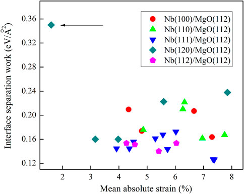
The optimized lattice constants of MgO and Nb unit cells are 4.288 Å and 3.408 Å, respectively. We build 27 calculation models constructed by Nb films and the MgO(112) substrate. The calculation results of interface separation works for all models are shown in Figure 2. In this figure, the transverse axis is the two-dimensional mean absolute strain ((|ε11|+|ε22|+|ε12|)/3) of the Nb slab, and the vertical axis is the value of Wsep. One model has the biggest interface separation work (0.35 eV/Å2) among all calculation models, as indicated by the black arrow. This calculation model belongs to Nb(120)/MgO(112), implying that the preferred growth direction of Nb films on the MgO(112) substrate is [120]. Early works showed that the preferred growth directions of Nb films on MgO(100), (110), and (111) substrates are [100], [112], and [110], respectively (Fu et al., 2014; Fang et al, 2016). The growth direction on the MgO(112) substrate is different from the situations in Nb/MgO(100), Nb/MgO(110), and Nb/MgO(111). Thus, this result gives a new strategy for adjusting the crystallization behavior of Nb films.
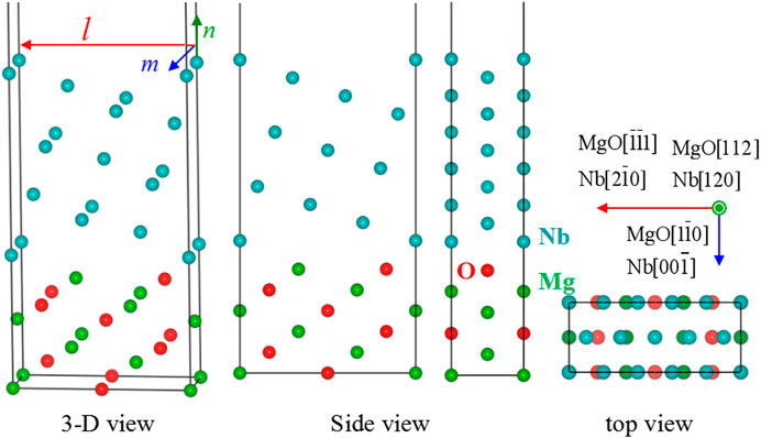
Figure 3 shows the crystal structure of the calculation model with the biggest Wsep. In this model, l, m, and n directions are perpendicular to each other, and the orientation relationships along l, m, and n directions are Nb [
3.2 Formation mechanism of the preferred Nb/MgO interface
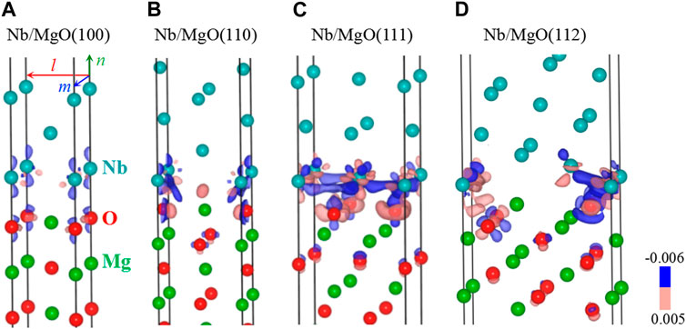
The interface structures of Nb/MgO(110), Nb/MgO(110), Nb/MgO(111), and Nb/MgO(112) are analyzed to explore the formation mechanism of the preferred interface. The calculation results of the electron density difference, together with the crystal structures, are shown in Figure 4. First, electrons are transferred from Nb slabs to MgO slabs in the four structures, and the transformation mainly occurs between the two layers that are near the interface, as indicated by the blue and red isosurfaces. This means that the chemical bonds at the interface are mainly ionic bonds. The interface bonding strength is mainly determined by the atomic configuration of the two layers that are near the interface. Meanwhile, from the local distribution of charge density, the Nb atom loses its electrons, while the O atom in the first layer of the substrate gains electrons. The chemical bonding along the interface is an Nb–O ionic bond. In addition, the number of charge transfers in the Nb/MgO(111) system is the largest, and the number of charge transfers in the Nb/MgO(100) system is the smallest, indicating that the interface bonding strength of the Nb/MgO(111) system is the largest, while the interface bonding strength of the Nb/MgO(100) system is the weakest.

FIGURE 4. Interface structures and electron density difference calculation results of Nb/MgO(100) (A), Nb/MgO(110) (B), Nb/MgO(111) (C), and Nb/MgO(112) (D). The electron density isosurfaces of the blue and red regions are −0.006 and 0.005 e/Bohr3, respectively.
Second, the atomic matches along the interface are different in the four structures. To be specific, Nb atoms are located on the top of O atoms that are present in the first layer of MgO(100) in Nb/MgO(100) (Figure 4A); Nb atoms are located on the top of Mg atoms that are present in the second layer of MgO(110) (Figure 4B); Nb atoms are located on the top of O atoms that are present in the third layer of O-terminated MgO(111) (Figure 4C); and Nb atoms are located on the top of Mg atoms that are present in the sixth layer of MgO(112) (Figure 4D). However, there is a hidden rule about the atomic matches in the four interfaces. Nb atoms in the first layer of Nb slabs are all located on the most stable adsorption positions of the MgO surface. For example, the most stable adsorption position for Nb atoms on the MgO(100) surface is on the top of the O atom, and the most stable adsorption position for Nb atoms on the MgO(110) surface is on the top of Mg atoms present in the second layer. Thus, it can be deduced that the specific atomic configuration of the MgO surface determines the atomic arrangement of the first layer of the Nb film and further determines the preferred growth direction and interface structure of Nb/MgO.
4 Conclusion
In summary, we predicted the preferred interface structure between Nb thin films and MgO(112) substrates (Nb/MgO(112)) by using the first-principles calculation method and compared it with Nb/MgO(100), Nb/MgO(110), and Nb/MgO(111). The results showed that the preferred growth direction of Nb films on MgO(112) is [120], and the interface type is very possibly coherent. Further analysis shows that the unique atomic configuration of the MgO surface could be the determining factor for the interface structure of Nb/MgO.
Data availability statement
The original contributions presented in the study are included in the article. Further inquiries can be directed to the corresponding author.
Author contributions
PM, YF and HZ designed the work. JY performed the simulations and wrote the manuscript. PM, SB, and YJ analyzed the data and corrected the manuscript.
Funding
This work was supported by the Malaysian Ministry of Higher Education under the Fundamental Research Grant Scheme (FRGS/1/2019/STG01/UMS/02/2), the Opening Project of State Key Laboratory for Mechanical Behavior of Materials (No. 20212304), the Opening Project of Material Corrosion and Protection Key Laboratory of Sichuan Province (No. 2020CL15), and the Talent Introduction Project of Sichuan University of Science and Engineering (No. 2017RCL34).
Acknowledgments
The authors thank Xiangdong Ding of Xi’an Jiaotong University for insightful discussions and calculation assistance.
Conflict of interest
The authors declare that the research was conducted in the absence of any commercial or financial relationships that could be construed as a potential conflict of interest.
Publisher’s note
All claims expressed in this article are solely those of the authors and do not necessarily represent those of their affiliated organizations, or those of the publisher, the editors, and the reviewers. Any product that may be evaluated in this article, or claim that may be made by its manufacturer, is not guaranteed or endorsed by the publisher.
References
Baski, A. A., Erwin, S. C., and Whitman, L. J. (1995). A stable high-index surface of silicon-Si(5 5 12). Science 269 (5230), 1556–1560. doi:10.1126/science.269.5230.1556
Chen, L., Li, Y. F., Xiao, B., Gao, Y. M., Wang, J., Yi, D. W., et al. (2021). Chemical bonding, thermodynamic stability and mechanical strength of Ni3Ti/α-Al2O3 interfaces by first-principles study. Scr. Mater 190, 57–62. doi:10.1016/j.scriptamat.2020.08.021
Du, J. L., Fang, Y., Fu, E. G., Ding, X., Yu, K. Y., Wang, Y. G., et al. (2016). What determines the interfacial configuration of Nb/Al2O3 and Nb/MgO interface. Sci. Rep. 6, 33931. doi:10.1038/srep33931
Du, J. L., Zhang, L. Y., Fu, E. G., Ding, X., Yu, K. Y., Wang, Y. G., et al. (2017). Comparison of interface structure of BCC metallic (Fe, V and Nb) films on MgO (100) substrate. Appl. Surf. Sci. 410, 585–592. doi:10.1016/j.apsusc.2016.10.117
Ernst, F. (1995). Metal-oxide interfaces. Mat. Sci. Eng. R. Rep. 14 (3), 97–156. doi:10.1016/0927-796x(95)80001-8
Fang, Y., Zhang, L. Y., and Zhang, H. L. (2016). Predicting the interface structure of Nb thin film grown on MgO(110) substrate. Mat. Lett. 183, 338–340. doi:10.1016/j.matlet.2016.07.101
Finnis, M. W. (1996). The theory of metal-ceramic interfaces. J. Phys. Cond. Matt. 8 (32), 5811–5836. doi:10.1088/0953-8984/8/32/003
Fu, E. G., Fang, Y., Zhuo, M. J., Zheng, S. J., Bi, Z. X., Wang, Y. Q., et al. (2014). Interface structure of Nb films on single crystal MgO(100) and MgO(111) substrates. Acta Mater 64, 100–112. doi:10.1016/j.actamat.2013.11.031
Han, X. L., Liu, P., Sun, D. L., and Wang, Q. (2020). The role of incoherent interface in evading strength-ductility trade-off dilemma of Ti2AlN/TiAl composite: A combined in-situ tem and atomistic simulations. Compos. Part B 185, 107794. doi:10.1016/j.compositesb.2020.107794
Hocker, J., Cartas, W., Schaefer, A., Baumer, M., Weaver, J. F., Falta, J., et al. (2015). Growth, structure, and stability of the high-index TbOx(112) surface on Cu(111). J. Phys. Chem. A 119 (25), 14175–14184. doi:10.1021/acs.jpcc.5b02463
Lairson, B. M., Visokay, M. R., Sinclair, R., Hagstrom, S., and Clemens, B. M. (1992). Epitaxial Pt(001), Pt(110), and Pt(111) films on MgO(001), MgO(110), MgO(111) and Al2O3(0001). Appl. Phys. Lett. 61 (12), 1390–1392. doi:10.1063/1.107547
Lu, L., Chen, X., Huang, X., and Lu, K. (2009). Revealing the maximum strength innanotwinned copper. Science 323 (5914), 607–610. doi:10.1126/science.1167641
Quan, Z. W., Wang, Y. X., and Fang, J. Y. (2013). High-index faceted noble metal nanocrystals. Acc. Chem. Res. 46 (2), 191–202. doi:10.1021/ar200293n
Schonherr, H. P., Notzel, R., Ma, W. Q., and Ploog, K. H. (2001). Evolution of the surface morphology of Fe grown on GaAs (100), (311)A, and (331)A substrates by molecular beam epitaxy. J. Appl. Phys. 89 (1), 169–173. doi:10.1063/1.1330556
Shikada, K., Ohtake, M., Kirino, F., and Futamoto, M. (2009). Microstructure and magnetic properties of FeCo epitaxial thin films grown on MgO single-crystal substrates. J. Appl. Phys. 105 (7), 07C303. doi:10.1063/1.3067854
Wang, S. G., Ji, X. X., Ao, Y., and Yu, J. (2018). Substrate-orientation dependent epitaxial growth of highly ordered diamond nanosheet arrays by chemical vapor deposition. Nanoscale 10 (6), 2812–2819. doi:10.1039/c7nr07100k
Keywords: interface structure, coherent interface, Nb/MgO(112), high-index plane, first-principles calculation
Citation: Yang J, Moh PY, Baco S, Jin Y, Fang Y and Zong H (2023) Interface structure between Nb thin film and MgO(112) substrate: A first-principles prediction. Front. Mater. 10:1158697. doi: 10.3389/fmats.2023.1158697
Received: 04 February 2023; Accepted: 15 March 2023;
Published: 03 April 2023.
Edited by:
Francesca Casoli, National Research Council (CNR), ItalyReviewed by:
Yunjiang Wang, Institute of Mechanics (CAS), ChinaAkshay Murthy, Fermi National Accelerator Laboratory (DOE), United States
Copyright © 2023 Yang, Moh, Baco, Jin, Fang and Zong. This is an open-access article distributed under the terms of the Creative Commons Attribution License (CC BY). The use, distribution or reproduction in other forums is permitted, provided the original author(s) and the copyright owner(s) are credited and that the original publication in this journal is cited, in accordance with accepted academic practice. No use, distribution or reproduction is permitted which does not comply with these terms.
*Correspondence: Pak Yan Moh, cHltb2hAdW1zLmVkdS5teQ==; Hongxiang Zong, em9uZ2h1c3RAMTI2LmNvbQ==
 Jun Yang1,2,3
 Pak Yan Moh
 Yong Fang
