 Urvashi Sharma
 Gulshan Kumar1,3
 Sachin Mishra
- 1Division of Research and Development, Lovely Professional University, Phagwara, Punjab, India
- 2School of Electronics and Engineering, Lovely Professional University, Phagwara, Punjab, India
- 3School of Computer Science and Engineering, Lovely Professional University, Phagwara, Punjab, India
- 4School of Chemical Engineering and Physical Sciences, Lovely Professional University, Phagwara, Punjab, India
The semiconductor industry is actively looking for an all-encompassing memory solution that incorporates the advantageous aspects of current technology. This features non-volatility, like that of Flash memory, high scalability, like that of both Dynamic Random Access Memory (DRAM) and Flash, quick operation, like that of Static RAM (SRAM), and durability, like that of both DRAM and SRAM. Ferroelectric thin films, which have electrically switchable bi-stable polarization, are one prospective technology that has the potential to revolutionize memory storage. However, due to difficulties with scalability and dependable industrial manufacturing, Ferro-Electric (FE) memory technology has not been able to effectively compete with DRAM and Flash. Research in this area has accelerated after the recent discovery of resistive switching in ferroelectric tunnel junctions (FTJs). For FTJs to be successful, it is important to overcome some obstacles, such as preserving bi-stability in ferroelectric thin films over the critical thickness. Additionally, the existence of interfacial layers, sometimes known as a “dead layer”, between the electrode and the film can affect its characteristics. The article gives an overview of semiconductor memories with an emphasis on emerging technologies having the potential for future applications. It then goes into detail on the benefits of FTJ and its non-destructive reading capacity. The article also discusses the potential uses for FTJs in resistive switching while acknowledging their drawbacks and constraints.
1 Introduction
Information storage systematically evolved from the oldest memory devices such as “Analogue Rosetta Stone” to “Digital storage devices” that realize data preservation, data recovery, and document reconstruction. At present, the need for digital memory with greater capabilities is increasing at an exponential rate, and the semiconductor industry is changing to accommodate the future requirement of information technology. The Internet of Everything (IoE)works in a synchronized way with other technologies like artificial intelligence (AI), machine learning (ML), internet of things (IoT), big data, cloud, fog, edge computing and communication devices, routers, sensors, etc., cannot be powered without non-volatile semiconductor memories. Therefore, it would be incorrect to consider the semiconductor memory sector to be a matured technology devoid of offering extreme devices of current requirements. The power consumption of high-frequency operated logic and memory devices, smartphones, and microelectromechanical systems has increased as the number of transistors has increased by the vertical shrinkage in dimension. These devices have a smaller lateral die size and a gradually rising storage density. At present, any electronic system that uses memory to store information is based on a semiconductor substrate. Due to the demand for more storage density, memory technologies have been expanded into various types. To meeting the global demand for non-volatile data storage, there are memory technologies, that are emerging memories since the realization of proof of concept, like Ferroelectric RAM (F-RAM), Magnetic RAM (MRAM), and Resistive RAM (RRAM) (Jeong and Hwang, 2018; Chen et al., 2023; Cappelletti, 2015). However, the non-volatile memory devices that need to be created in the present scenario must be, quick, energy-efficient, dense, robust, and radiation-resistant to meet the long-term operational requirements.
Several semiconductor memory technologies are outlined in Figure 1 and are briefly discussed as follows before discussing the ferroelectric tunnel junction (FTJ) for high-density memories. These memories can be classified into two main groups, namely, volatile and non-volatile memories. Read-only memory (ROM) and random-access memory (RAM) are two categories of semiconductor technology embrace the aforementioned classification. Historically, RAM, a volatile memory, is utilized by the central processing unit (CPU) of the computers to write and read data in the predetermined order that involves a random draw of information from the memory. With this kind of memory, data can be stored and read numerous times at relatively high speed compared to secondary memory devices like hard disks. Volatile memory is a term used to describe memory that loses its contents when the power is switched off. Memory types that are volatile include, dynamic random-access memory (DRAM), Mobile DRAM (MDRAM), static RAM (SRAM), and Synchronous DRAM (SDRAM). One capacitor and one transistor make up basic cell of the DRAM’s structure and 1 bit of information per cell is stored in the capacitors. When a capacitor is charged, it achieves logic “1,” whereas a capacitor that has been discharged has a logic “0.” However, six transistors are used in the construction of the SRAM, of which two are cross-coupled transistors and the other four are pass transistors. Memory bits are stored in the cross-coupled transistor pairs, which are Complementary Metal Oxide Semiconductor (CMOS) inverter pairs. In addition to this six-transistor arrangement, SRAM also has four other transistor configurations. High-impedance resistors are used to replace the p-MOS in this design. SRAM is used in cache memories, while DRAM is used in the primary memories. In contrary, even when the power is off, information is stored permanently in ROM and hence it is a non-volatile memory (Fujisaki, 2013). A computer’s ROM contains the basic input/output system (BIOS) program, a software run fist when you start the computer. Erasable Programmable ROM (EPROM), Electrical Erasable Programmable ROM (EEPROM), ultraviolet programmable ROM (UVPROM) are other variants of ROM used for the information storage. However, major development in the non-volatile memory category occurred at Bell Laboratory, by Kahng D and Sze SM. They originally proposed the floating gate transistor (FGT) as a non-volatile memory component in 1967 and that was the beginning of MOS’s expansion into the nonvolatile device. Flash memory is built on FGT, a type of metal oxide semiconductor field emitter transistor (MOSFET) with one minor modification: an additional gate is inserted between the control gate and the body. This additional gate is referred to as a “floating gate” (FG). Since there are no electrical contacts and it is electrically isolated, any charge injected into the FG will stay there for many years. To encode data using a charge state, it enables flash memory devices to store data as a collection of charges. The FGT has two states: a) a negative charge; and b) a zero charge (Gerardin and Paccagnella, 2010; Hamdioui et al., 2017). A “0” bit value is assigned to the negative charge state and a “1” bit value to the zero-charge state. The two types of flash memory are NOR (huge cell size and direct write) and NAND (small cell size and page write). NAND flash memory frequently takes the place of storage memory in the form of a hard disc memory. When compared to DRAM, which is made up of 1T-1C, NAND flash memory’s double gate transistors structure makes it appropriate for high-density memory storage with a smaller cell size. NAND flash is not a good choice for working memory due to its limitations on longevity (105 cycles) and slower writing speed (ms), apart from its ability to store data and programs without power. The most popular and reliable portable secondary memory type is flash memory. Solid-state memory technologies like DRAM, SRAM, and Flash have dominated the semiconductor memory market for the past 40 years of its development (Jeong et al., 2012). Figure 1 also shows the classification of various memories based on their functioning characteristics with additional reference to the new and emerging technologies. In the non-volatile memory category, emerging technologies for future memory formats includes resistive RAM (RRAM), phase change RAM (PCRAM), magnetic RAM (MRAM), Spin-transfer torque MRAM (STTMRAM), and ferroelectric RAM (Fe-RAM) aim to compete with DRAM and SRAM (Gerardin and Paccagnella, 2010; Hamdioui et al., 2017).
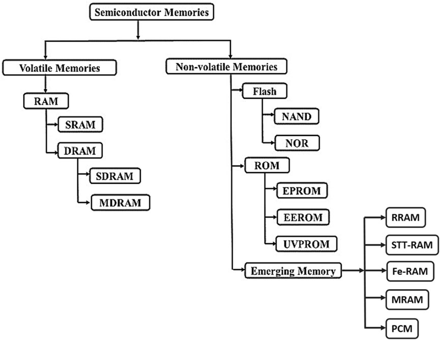
FIGURE 1. Classification of memory technologies concerning their functional aspects.
From the emerging memories, an intermediate endurance of 1010–1012 and density in gigabyte (GB) can be achieved phase change random access memory (PcRAM or PCM). PcRAM’s foundation is the materials like chalcogenides’ reversible shift from low resistance (crystalline phase) to high resistance (amorphous phase). The design of the memory cell and the characteristics of the phase-change materials affect performance memory cell. PcRAM cells must be configured to meet the needs of increased thermal isolation, reduced reset current, easy processing, and power efficiency. Materials utilized in PcRAM with several nm thin-film thicknesses or nanoparticle diameters are used to exhibit the desired scaling behavior, which includes high crystallization temperature at a smaller dimension and decreasing thermal conductivity (Gerardin and Paccagnella, 2010; Law and Wong, 2021a). The substantial switching current restricts the linear dependency of the threshold voltage. Despite experimental testing using bipolar junction transistor (BJT) and diode devices, the efforts to shrink the cell size of phase-change random access memory (PcRAM) encountered obstacles such as electrode void development, elements segregation, and changes in mass density. However, the development showcased remarkable features, including a fast-switching speed of 100 nanoseconds and an endurance of over one billion cycles (>109) in the case of PcRAM (Fujisaki, 2013; Hamdioui et al., 2017). Nevertheless, PcRAM is unable to displace Flash memory or dynamic random-access memory (DRAM) primarily due to two factors: manufacturing costs and the continuous advancements within existing memory technology. Constant improvements in performance, density, and cost-effectiveness contribute to a competitive environment. These factors collectively make it difficult for PcRAM to surpass Flash and DRAM in terms of popularity and market dominance.
Apart from the aforementioned phase change memory (PCM), resistive random-access memory (RRAM) has been investigated for creating synaptic devices inside 3D cross-point designs. RRAM is a good contender for memory operations because the ion-based process controlling inductance in it mimics the synaptic plasticity seen in biological systems (Fujisaki, 2013). Operations for filamentary conductive-bridging RRAM (CBRAM) and oxide RRAM (ox RAM) (Goux, 2019; Garbin et al., 2015) are controlled by the growth and breakdown of a conductive filament (CF) made of oxygen ions and cations diffused through the material. The homogenous movement of oxygen ions/vacancies across the layer stack is a key component of the oxide RRAM, influencing aspects like the tunneling/Schottky barrier’s thickness and barrier height. However, the precise process causing barrier modulation is still being debated. A number of options are being investigated, including phase change, redox/oxidation, electrostatic effects, and modifications to the local oxide stoichiometry. A multiscale modeling platform is used to relate the performance of electrical devices to atomic material attributes in order to comprehend the behavior of RRAM devices (Larcher and Padovani, 2017; La Torraca et al., 2019; Padovani et al., 2017). This platform accounts for the individual contributions of ions and vacancies/drifts and their effects on power dissipation and local temperature. Consideration of different charge transport processes such tunneling, drift and diffusion, and hopping also accounted. Aside from the bond deformation, breaking, chemical reactions, diffusion of atomic vacancies and interstitial ions, and phase shifts, the modeling also takes into account material variations at the atomic level.
Emerging memory is motivated by overcoming these problems and is the subject of active research (Law and Wong, 2021a; Lankhorst et al., 2005). However, characteristics like low power consumption, non-volatility, density, and speed are necessary for the development of future semiconductor memories. Such a memory prowess might lead to the development of a “universal memory” that will combine the non-volatile properties of FLASH, the long durability of DRAM and SRAM, the fast speed of SRAM, and the great scalability of DRAM and Flash (see Tables 1 and 2). The ferroelectric capacitor of ferroelectric RAM, also known as FRAM or Fe-RAM is one of them, where ferroelectric material is sandwiched between two metal electrodes. With the ferroelectric layer replacing the dielectric layer, it is similar in design to DRAM and functions similarly to flash memory in terms of the non-volatility of the stored information (Law and Wong, 2021a). James Scott contributed significantly to the advancement of ferroelectric memories as the co-founder of Symmetrix. He oversaw the development of integrated thin film ferroelectric technology suited for microelectronic devices from bulk ceramic technology. The discovery that the Aurivillius class of ferroelectrics, illustrated by SrBi2Ta2O9 (SBT), does not suffer polarization fatigue a behavior different from that of traditional perovskite ferroelectrics was one of his major accomplishments (Chen et al., 2018). The drawbacks of FeRAM are the high manufacturing costs due to CMOS incompatible material and poor storage density compared to DRAM. Currently, Fe-RAM uses in motion control, process controls in industries, wireless data logging, gamma radiation in wireless memory, and radio frequency identification (RFID). Other applications include advanced metering, gaming, point-of-sale systems, automotive shift-by-wire, navigation, and anti-pinch control. The ferroelectric memory is set up with a ferroelectric field effect transistor and a ferroelectric capacitor, 1C, and 1T, respectively (Fe-FET). Due to the double-gate transistors NOR architectural construction, the memory has the potential to replace DRAM. The approach has not been implemented due to technical challenges like the need for thin enough ferroelectric thin films of less than 10 nm in the capacitor (Fe-RAM) and transistor (Fe-FET) forms. Ferroelectric layers make up the Fe-gate FET’s dielectrics. Ferroelectric polarization in Fe-FETs is used in place of a floating gate, comparable to Flash memory (Shin, 2005; Prall, 2007). The thin doped HfO2 films (< 5 nm) used in transistors and capacitors were developed by the Namlab in Germany. These are now accepted industrial standards, and doped HfO2 will be moving toward this specific goal. Parts of “ferroelectric memory” include ferroelectric tunnel junction (FTJ).
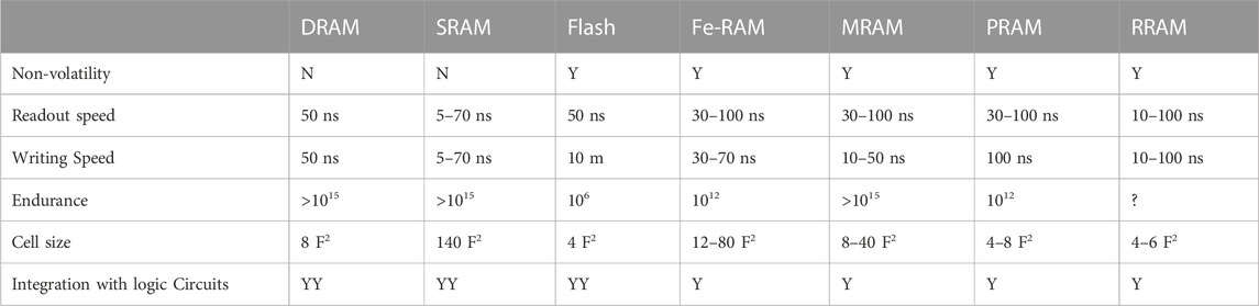
TABLE 1. The general characteristics of different memories available in the market.
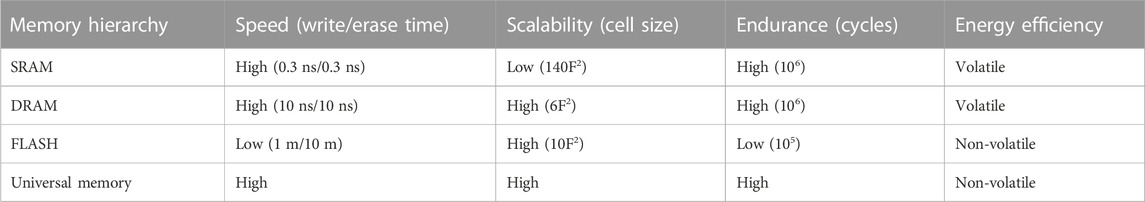
TABLE 2. The characteristics required for universal memory.
This represents a significant advancement in the field since it shows that efforts have been made to match the properties and functions of doped HfO2 with accepted performance and utility standards.
The ferroelectric tunnel junction (FTJ), a key element, plays a critical function in the larger field of memory technology. This component embodies the idea of ferroelectric memory, which uses tunneling mechanisms to store and retrieve data by manipulating the ferroelectric polarization state. In terms of improved data storage, preservation, and processing capabilities, FTJs represent a possible route for the development of memory technologies by utilizing the properties of ferroelectric materials. It is clear that the industry is expanding significantly outside the boundaries of known technologies in response to the rising demand for the newest memory solutions. This wave of development includes a variety of innovations, including:
The popularity of quantum dots (Q-dots) (Chauhan, 2007) is growing as a result of their distinctive electrical and optical characteristics. Through the use of efficient data manipulation techniques and high-density data storage made possible by quantum mechanical processes, quantum dots have the potential to revolutionize memory technology. A number of cutting-edge methods in memory technology are set to change how data is processed and stored. Zero-RAM stands out as a ground-breaking idea that goes against the grain of RAM technology conventions (Amo-Boateng, 2017). Zero-RAM promises to improve data access speeds while simultaneously lowering power consumption by focusing on eliminating intrinsic constraints. By tackling basic flaws and ushering in a new era of effective and high-performance memory systems, this dual approach has the potential to transform memory solutions. Stochastic Phase-Change-Based Memory (SPBMM), another ground-breaking challenger, makes significant gains by utilizing the concepts of phase-change materials. Optimizing data retention, increasing energy economy, and optimizing system performance are all objectives of SPBMM’s design (Tuma et al., 2016). By utilizing the distinct qualities of phase-change materials, SPBMM has the ability to satisfy the requirements of contemporary computer environments, which call for dependable, quick, and energy-efficient memory solutions.
By introducing transformational capabilities, as demonstrated by this combination, memory technology and its applications across multiple industries could undergo a revolution. Together, these cutting-edge memory technologies herald an exciting new era of technological development, promising to revolutionize how data is stored. Collectively, these cutting-edge memory technologies herald an exciting new era of technological development that will push computing as know it to new heights by revolutionizing how data is stored, accessed, and processed (Lankhorst et al., 2005). The spike in interest and investment in these next-generation memory technologies highlights the industry’s acknowledgment of the necessity for cutting-edge solutions as the market continues to diversify and adapt. These developments have the potential to completely alter the memory technology landscape, opening up new opportunities for data-driven enterprises and altering the course of technological development.
1.1 Universal memory
Technologies like SRAM have outstanding read and write speeds (0.3 ns/0.3 ns) and require less power (Sharma et al., 2021; Liu et al., 2021). Since it requires a lot of foot print area due to the huge size of the cell typically six transistors, makes it unsuitable for embedded applications. DRAM has a denser architecture than SRAM since it only has one transistor and one capacitor per cell. For updating the bit state in DRAM every few milliseconds, constant power is required. This serves to stop the leaking of charges that are stored in the capacitor. DRAM in portable electronic devices shorten the battery life due to its high-power consumption. However, Flash memory provides information storage that is not volatile. The production process is complicated despite its high density and requirement for high-voltage driving circuits for embedded applications. This also results in slower write and erase operations (1 ms/0.1 ms) (Hemavathy and Meenakshi, 2017). The use of DRAM with a single transistor, commonly known as zero-capacitance RAM, is necessary to overcome some scaling challenges (Fujisaki, 2013). Although this kind of memory solves the scaling issues, its use as universal memory is constrained by the drawbacks such volatile ionization ignition and the need for high operating voltage. Therefore, scientists are working to create memories that get around these constraints by developing memories that are non-volatile like FLASH memory, highly scalable like DRAM and FLASH, fast like static random-access memory (SRAM), and durable like DRAM and SRAM. It has long data retention, scalability to meet growing technological demands of high density, quick access times for quick data retrieval, and durability to survive repeated read and write operations. This perfect memory ‘universal memory’ would incorporate the greatest attributes of many memory kinds. By meeting these objectives, researchers hope to create a memory technology that transcends the constraints of available choices and provides a flexible and effective solution for a range of applications.
Magneto resistive RAM (MRAM) (Sousa and Prejbeanu, 2005; Suzuki and Swanson, 2015; Senni et al., 2016) is promising with universally appealing properties like, high read and write speeds combined with non-volatile memory that has limitless endurance. The magnetoresistance of CoFeB/MgO/CoFeB based magnetic tunnel junctions found to be 230% or more is ideal for the high density MRAM (Chen et al., 2023). However, most obvious issues are the long-term stability of magnetic layers, ultrathin tunnel barriers, and data retention. With a high breakdown voltage and a very thin layer of aluminum oxide as the tunneling barrier in MRAM found to be stable (Åkerman, 2005; Yuasa and Djayaprawira, 2007). Over time, the inter-diffusion layers between the magnets have an impact on the switching performance. According to the results of the accelerated test, the switching performance of MRAM will not change over the course of 10 years (Kokado and Harigaya, 2003). Motorola unveiled the single transistor and tunnel junction MRAM in 2002 with Read-and-write cycles of 50 ns For many years, companies like Siemens, Motorola, Hitachi, and Hewlett Packard have done extensive studies on the problems with MRAM addresses. However, the memory producers are still not ready to begin mass-producing MRAM. One such difficulty is the non-uniformity of the insulating barrier. This is so that both the barrier’s thickness and the direction of relative magnetization are impacted by the resistance of tunnel junctions. Due to thermal fluctuations, super-para-magnetism with small magnetic particles raises concerns about the loss of magnetic information. For the discovery of fully universal memory based on magnetic tunnel junction, significant advancements are required. The production of Spin-Transfer Torque (STT) MRAM (Sharma et al., 2021; Marinella, 2014), in which individual electrons are used to represent 1s and 0s to adjust the magnetic orientation of cells in MRAM, has been jointly undertaken by Samsung, IBM’s Flexible Foundries of Memory and IBM’s Spin-Transfer Memory. This could expand the application’s market to include more mobile and IoT devices in addition to the sensor controller of Sprite Sats. Thus, a basic strategy for strengthening and upgrading the performance of current MRAM technology is required to realize “universal memory” with magnetic tunnel junctions.
The Laboratory of Functional Materials and Devices for Nano electronics at the Moscow Institute of Physics and Technology (MIPT) has information on the potential of the insulator hafnium oxide (Fabian et al., 2017; Ambriz-Vargas et al., 2017a; Abuwasib et al., 2015). The MIPT memory technology has been demonstrated to be faster than SRAM and to have a lower potential power consumption and non-volatile similar technologies. Hafnium dioxide is used as the storage medium in these developments at Sema Tech research centers (Bettinger et al., 2020; Kingon et al., 2000). It was accomplished by modifying the resistance using conductive filaments. RRAMs made of titanium dioxide have not yet reached commercialization despite 8 years of study by Hewlett Packard and Hynix, a major memory manufacturer in Korea.
FRAM is another contender for global memory that Texas Instruments (TI) has developed (Abdullaev et al., 2020; Mueller, 2018). With the elimination of memory hierarchy and the ability to sense vibration, pressure, temperature, motion, humidity, and pollution, TI has been converted into a compact microcontroller that may be used for field data loggers. As a challenger to SRAM that offered Fe-accelerating RAM’s speed, reduced power requirements, non-volatility of flash, and decreasing DRAM size, TI pitched Fe-RAM as a high-performance memory architecture that could also function as universal memory. The inventors of magneto-electric memory technology are from the Cornell University (Roco et al., 2011). By using electric potential alone, the magnetic and ferroelectric properties of MRAM and FRAM, based on multiferroic material, can flip from 1 to 0 with less energy. In more recent research, interest in ferroelectric memory has been intensified due to the ferroelectric characteristics of CMOS compatible doped HfO2 and HfZrO2 ultra-thin films in tunnel junction (Chen et al., 2021; Hur et al., 2022). In the framework of 3D neuromorphic computing systems, ferroelectric tunnel junctions (FTJs) based on HfO2 are being investigated for non-volatile memory applications (Tsymbal and Kohlstedt, 2006; Kolhatkar et al., 2018; Kolhatkar et al., 2019). The research shows simulation-captured hysteresis behavior in the form of tunneling I-V curves for FTJs based on 9-nm ferroelectric HfO2 (Kim et al., 2023). In FTJ, polarization reversal allows for a change in tunneling resistance in ultra-thin films (< 3 nm). With an overview of the various resistance states, it is a possible application in non-volatile memory. Since FTJ is significantly more developed than FeFET, it is covered in detail in this study. This combination of silicon-based technology with ferroelectric thin film offers the possibility of combining DRAM’s quick read and write capabilities while keeping the latter memory’s size modest and non-volatile.
2 Ferroelectric tunnel junctions
Esaki was indeed ahead of his time when he proposed a polar switch in 1971 that used a switchable thin-film ferroelectric material (Maksymovych et al., 2009; Mikolajick et al., 2021; Mikolajick et al., 2022). However, there were constraints on experimental methods and the ability to create high quality ultra-thin film of ferroelectric materials that could act as tunneling barriers at that time. It was also widely accepted that the critical thickness needed for ferroelectricity in thin films was substantially greater than the thickness required for tunneling (Abuwasib et al., 2015). Ferroelectricity was thought to disappear at critical thicknesses considerably below the nanometer range, so it was disregarded for about 30 years. It was not until 2003 that nanoscale ferroelectricity in ultrathin films with a few unit cells of thickness was proven to exist (Gao et al., 2017; Jia et al., 2007). This discovery opened the intriguing possibilities for ferroelectric tunnel junctions (FTJs) by producing thin films with ferroelectric characteristics that are appropriate for tunneling, which was reported in the scientific literature (Jia et al., 2007). Polarization reversal caused by the application electric field can quickly affect the conductance of FTJ. When the applied field matches the coercive field of the ferroelectric, this will lead to resistive switching. At the electrode barrier contact, polarization reversal changes the sign of the polarization charges (Ambriz-Vargas et al., 2017b). The FTJ structure with the Ferroelectric (FE) barrier can be seen in Figure 2. These are anticipated to have different current-voltage properties than typical tunnel junctions with dielectric barrier layer (Park et al., 2015).
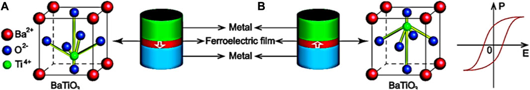
FIGURE 2. The basic construction of a typical FTJ. (A) BaTiO3 is used as an example to demonstrate the polarized ferroelectric barrier’s lattice on the left and right sides, (B) The ferroelectric barrier’s polarization-electric field (P–E) hysteresis loop.
In 2009, scanning probe microscopy was used to observe the Tunneling Electro resistance (TER) effect experimentally in ultrathin BaTiO3 (BTO) utilizing conductive tips and metallic oxides as the top and bottom electrodes (Gao et al., 2012; Dubourdieu et al., 2013). Following that, several FTJ structures with various ferroelectric materials and electrodes were suggested and elaborated in the literature. A ferroelectric ultrathin film sandwiched between two metals makes up the majority of an FTJ’s (Huang, 2019; Fey et al., 2021) core structure (M/FE/M structure). Through the tunneling effect, the ferroelectric film serves as a barrier to control electrons to pass through. The cation’s displacement from its centrosymmetric position results in a spontaneous polarization in the ferroelectric barrier. One of two directions can be chosen for this spontaneous polarization. By using an external voltage or mechanical stress, polarization change can be accomplished reversibly. The probability of electron tunneling differs for the two opposing polarization orientations due to the variation of the barrier potential profile caused by polarization switching. It causes the junction resistance to switch non-between a high (ON) and a low (OFF) level and is known as Tunneling Electro resistance (TER) (Kokado and Harigaya, 2003). The OFF/ON resistance ratio is known as the TER ratio, the more is better for the reliable operations memory cell. Since spontaneous polarization can persist in the absence of an external voltage, allowing the FTJ remain in the ON and OFF state permanently to be used in non-volatile memories (NVMs).
Two conditions must be met to create a reliable FTJ, i.e., the ferroelectric layer must be thin enough to allow for electron tunneling, thickness below the tunneling regime (< 3 nm). It is also necessary for two ferroelectric/metal interfaces (either side of the barrier layer) to be asymmetrical to provide different potential barrier heights for different polarization orientations. Following are the specifics of the operating principle. In the absence of an applied voltage, Figure 3 shows the potential profile of an FTJ for the opposing polarization orientations. In this case, two metals (M1 and M2) are made with different materials to create asymmetric interfaces. The potential profile changes when ferroelectric polarization is reversed, as already mentioned. The following factors, among others, affect the potential profile: i) polarization reversal; ii) variation in barrier thickness brought on by the opposite piezoelectric action; and iii) modification of barrier/electrode interfaces brought on by insufficient polarization charge screening (Tsymbal and Kohlstedt, 2006). The third theme is thought to be the most important component causing the TER effect, as will be discussed later.
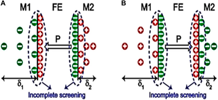
FIGURE 3. (A) Ferroelectric polarization, and (B) Depolarization caused by asymmetric charge screening (Wang L. et al., 2016; Yoon et al., 2019).
The ferroelectric polarization causes surface charges at the barrier/metal contacts, as seen in Figure 3A. The charges from the metals must screen out these surface charges. However, the screening is insufficient because, in each metal, the screening charges are typically distributed over a finite length away from the interface (shown by δ1 and δ2 in Figure 3), which is known as the screening length. The distribution of charges was predicated on the supposition that there is no other interface effect. Figure 3B shows that a depolarization field (Edep) opposing the ferroelectric polarization is created in this situation by the imperfect charge screening at the barrier/metal contacts. It is further hypothesized that the only source of the tilting of the electrostatic potential within the ferroelectric film is the depolarization field. The electrostatic potential at two barrier/metal interfaces is then asymmetric since the screening lengths for the two metals M1 and M2 are not identical, as shown in Figure 3A. A straightforward Thomas–Fermi model can provide the electrostatic potential profile (φ(x)) in these circumstances if the FTJ is short-circuited as Equation 1 (Ricci, 2015; Wang, 2015; Boyn, 2016):
where δ1 and δ2 are the Thomas–Fermi screening lengths in the materials M1 and M2, σs is the screening charge per unit area, ε0 is the vacuum permittivity, and d is the thickness of the FE film. The upper and lower signs signify situations with polarization toward M1 and M2, respectively.
With Equation 1 shown above, the opposite polarization orientations of the average potential barrier heights can be calculated as (Wang, 2015; Useinov et al., 2022; Cai et al., 2010):
where U is the total of all additional contributions to the potential profile, excluding φ (x).
As a result of δ1 and δ2, average potential barrier heights for the polarization orientations that are opposed to one another differ. As a result of the tunneling current’s exponential reliance on the square root of the potential barrier height, there are differences in tunneling resistances as well (Wang, 2015). The electrostatic potential at the interfaces, i.e.,
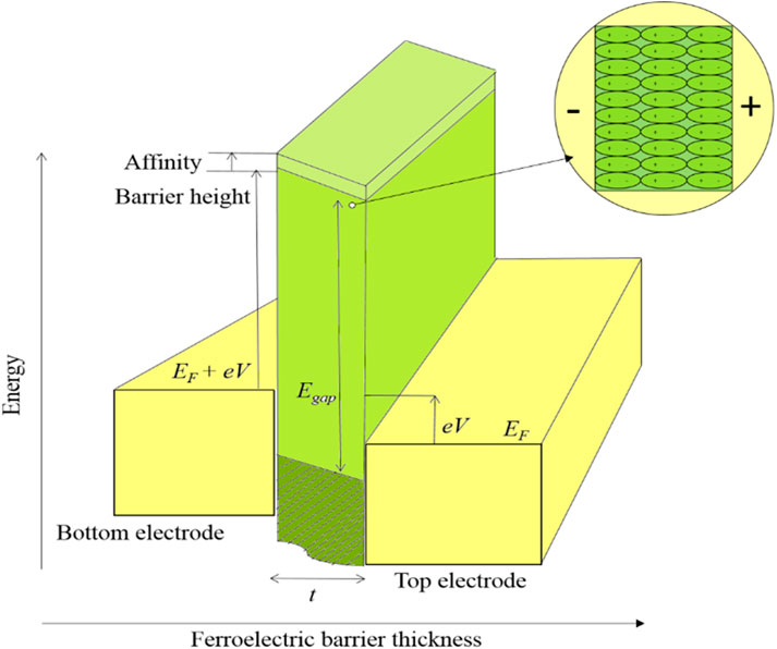
FIGURE 4. The pictorial representation of the ferroelectric tunnel junction with Egap is the energy gap, EF is the Fermi energy, V is the applied voltage, and t is the barrier thickness under the applied voltage (Tsymbal and Kohlstedt, 2006).
According to the results of the FTJ model Pt/BaTiO3/Pt studied, the ferroelectric switching-dependent tunneling conductance is influenced by changes in the bonding at the interface, the rate at which evanescent states decay, and the electrostatic potential at the barrier. The barrier’s inadequate screening as well as the FTJ’s interfacial and strain effects are clarified by the transmission functions and attenuation constant, respectively. An interfacial layer existence is due to atoms bounded to the electrodes. It has an impact on the barrier’s decay rate and, consequently, on the electron transmission through it. Barrier thickness changes and tunnel conductance are both impacted by the voltage applied across junctions (Tsymbal et al., 2012; Gruverman et al., 2009).
The polarization strongly depends on factors like strain, charge, and compositional variations and are the significant external factors. As discussed before, ultrathin barrier layers are necessary for the FTJ device’s manufacturing. Characterization and comprehension of ferroelectricity’s scaling are crucial. It was once thought that depolarization caused FE to vanish in films with a thickness less than 100 nm (Park et al., 2023; Morozovska et al., 2017). Because of this, FTJ was not practicable with oxide films thicker than 6 nm. Researchers, however, counter this with a minimum FE oxide thickness of 2.4 nm (Ezzaier et al., 2018; Martin et al., 2008). Wide gap oxide semiconductor also shows ferroelectricity. GaN or III-V, ZnO or II-VI with 3.4 eV, perovskite oxide BTO, SrTiO3 with 3.2 and 3.6 eV, and PTO with 2.9 eV band-gap have all demonstrated the same assertion (McCluskey and Haller, 2018). The qualities of TJ can be improved by the by selecting proper FE material. The FE polarization’s direction has an impact on resistive switching, making it possible to separate it from the well-known resistive switching of oxide materials (Wang et al., 2020; Pertsev and Kohlstedt, 2010). The BaTiO3 (BTO) films have already shown ferroelectricity to a thickness of 1 nm and 75,000% electro-resistance. M. Bibes and A. Gruverman published the TER effect’s initial experimental demonstration in 2009 (Tsymbal et al., 2012). BTO (Sulaev et al., 2015; Li et al., 2015) was utilized as an incredibly thin ferroelectric layer in both situations. The development of nondestructive polarization readouts as a result of the order 2 TER effect opened up new possibilities for nonvolatile memory technology. Although many oxides exhibit switching behavior, oxygen vacancies, grain boundaries, and dislocations can have an impact. The characteristics of the FE as a barrier layers influence the likelihood of transmission in the following ways: 1) piezoelectricity of the FE material of the barriers results in strain with applied voltage and changes the transport characteristics; 2) incomplete screening of the FE results in the electrostatic potential; and 3) B-site displacement results in the interface of atomic orbital hybridization that differs from orientation polarization, as in the case of the BTO/SrRuO3 interface. The conductance effect of this displacement affects the current-voltage characteristics of FTJ. The barrier/electrode interface is altered by the switch from +P to −P in polarization (as shown in Figure 5). It is difficult to determine whether polarization orientation and tunneling conductance are correlated. One of the issues with measuring conductivity with polarization changes and their experimental analysis utilizing the electro-resistance effect using the polarization control. Another challenge is the polarization stability of ultra-thin ferroelectric films barriers. Loss of polarization retention and relaxation of TER are brought on by the less effective polarization screening of oxide metal in comparison to normal metal. In line with the FE displacement of the barrier layer as BTO, the tunneling conductance significantly decreases. Apart from the inorganic oxides (Pb(Zr, Ti)O3, BTO, BFO, and (Ba, Sr)TiO3), TER effect was demonstrated by the organic barriers, specifically the copolymer films of polyvinylidene fluoride (PVDF) 70%-trichloroethylene (TrFE) 30% (Pawar et al., 2023). Researchers noticed the apparent change when the polarization was reversed and was accompanied by an I-V diode. The geometry suggested by Zhuralev et al. can be used practically and does not require the FTJ arrangement with electrodes (Wang et al., 2022). The tunnel profile in such a device is thought to represent a superposition of variable potential coming from the FTJ conduction band.
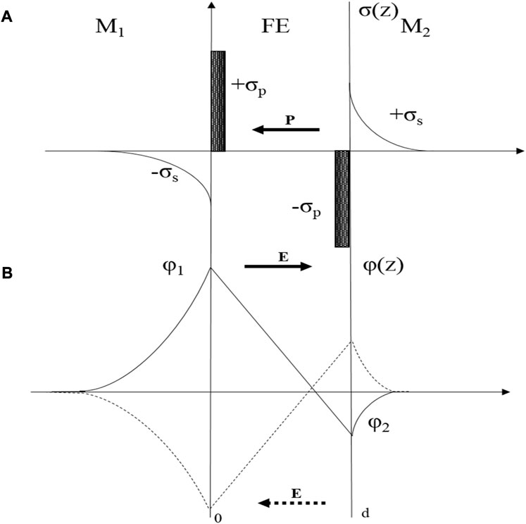
FIGURE 5. Electrostatic effect of M1-FE-M2: (A) The charge vs. distance distribution and their respective (B) profile of electrostatic potential vs. distance (dark line) (Gruverman et al., 2009).
2.1 Resistive memory with FTJ
A few binary as well as complex oxide materials show resistive switching (Jeong et al., 2012). Chua asserted the existence of the circuit component based on flux-linkage to charge way back in 1971 and gave it the name memory resistor (memristors), a non-linear resistor (Mouttet, 2012). The physical processes that led to the emergence of memory resistance in a material includes self-heating, chemical reactions, spin polarization, phase transitions, and ionic transfer. The construction of an additional barrier in a semiconductor showed memristive behavior in a metal/ferroelectric/semiconductor FTJ by the tunnelling modulations (Ricci, 2015; Wen and Wu, 2020). Multilevel memory and logic devices use the benefits of huge resistance switching effect, control of transport spin polarization, low operating power, non-destructive reading, scaling down to the nanoscale range, and programmable resistance (memristive). With Co/Pb(Zr,Ti)O3/(La0.7Sr0.3)MnO3, Pt/BTO/SrRuO3, (La0.67Sr0.33)MnO3/BiFeO3/(La0.67Sr0.33)MnO3, Cr/BTO/Pt, and Co/BiFeO3/LaNiO3, the behavior of TER may be investigated (Neumann et al., 2013; Zenkevich et al., 2013; Garcia and Bibes, 2020). The direction of polarization, which can be changed by an applied electric field, determines the resistance of the barrier. Because of this tunnel electro-resistance, ferroelectric states are not damaged by the reading. Examples of interface barriers with electrodes are STO at the interface of BTO/SRO, CoOx layer with Co/BTO interface (Wang et al., 2016). The stable polarization was established by Triscone and his team in Geneva using a 4-nm epitaxial film of the FE perovskite Pb(Zr0.2Ti0.8)O3 (Guyonnet et al., 2011). Using synchrotron radiation on PTO with a thickness of 1.2 nm, the Argonne National Laboratory examined the FE properties (Petkov et al., 2007). The surface accumulation of charges corresponds to a minimal ON state capacitance. Due to the presence of the space charge zone, the capacitance measured to the OFF state should be lower than the ON state. Tunable OFF state suggests the use of hetero-configurations of metal, ferroelectrics, and semiconductors in memristive devices (Wen et al., 2014). HfO2 and HfZrO2 films with 2 nm tested both maintain their ferroelectricity to 5 nm. A current density of 75 A/cm2 that is higher than previously reported values was measured at 0.1 V. This makes one of the promising applications for ultra-low-power NVMs due to the CMOS compatibility. Non-centrosymmetric orthorhombic structure of the thin films of HZO and HFO is responsible for the ferroelectricity (Sulaev et al., 2015; Li et al., 2015; Mo et al., 2018; Saitoh, 2020). Low ON/OFF ratio ferroelectrics have lower switching energies than those employing traditional junctions. The use of interfaces allows for a significant improvement in the ON/OFF ratio. Along with the FE barrier, these interfaces reduce depolarization field screening. This leads to polarization being unstable, which in turn affects the resistive switching’s retention characteristics. Interface modulation as a result results in 105% ON/OFF resistive switching. The memristors consist of two terminals, where resistance can be continually modified using the amplitude, duration, and electrical impulses that have already been applied. The Co/BFO/Ca0.96Ce0.04MnO3 (Fabian et al., 2017) (CCMO) fully integrated device was studied and large TER was observed. For calculating the potential, the model used Thomas–Fermi screening with a short-circuit boundary conditions screening tool. The electrostatic potential can be denoted as (Stengel, 2013; Hwang et al., 2020):
Where.
The interface potential and the screening charge can be determined from boundary conditions,
The tunneling conductance can be calculated using the Landauer formula for the FTJs per unit area:
The energy EF at the Fermi level gives the transmission coefficient of T(EF, kǁ) for a transverse wave factor kǁ. The potential developed across the boundary condition is obtained using the Schrödinger equation. The transmission coefficient of an electron moving with the potential V(z) of the incoming wave can be normalized to a unit flux density. The solution obtained numerically for V(z), the step-wise potential arises from the minimum conduction band and electrostatic potential superposition of ϕ(z) (Zhuravlev et al., 2009). The experiment showed the local transport of electrons on a thin ferroelectric film deposited on the metal layer using AFM. The controlled effect of the dielectric layer gives rise to new opportunities to modify TER. With the reversal of polarization, electrostatic potential changed and among the interface, non-polar film started acting as a switch for changing the barrier height from high to low values. It causes a change in transmission across FTJ. The orientation of the polarization-to-resistance ratio may reach large values (Zhuravlev et al., 2009). The current across the thick ferroelectric incorporates resistive and non-destructive readout of information with restricting miniaturization of circuits. The thickness of such ferroelectrics can be reduced to nanometers; hence their electric conduction enhancement becomes possible. The ferroelectric PTO tunnel barrier showed 50,000% TER through a 3.6 nm film (Bez and Pirovano, 2004; Fujisaki, 2013). When calculating the ER of a ferroelectric barrier film, the various transport mechanisms such as direct tunneling, thermionic injection, and Fowler-Nordheim tunneling (Chiou et al., 2001; Ikuno et al., 2011; Rumberg and Graham, 2013) are considered. These depend on the thickness of the barrier, the polarization’s direction, and the ferroelectric and metallic properties.
Large ER are presented by the yield with direct tunneling and FNT presented by the 5 nm BFO film, among others (Wen and Wu, 2020). Theoretical calculations, synthesis, and ferroelectric material research have inspired a focused investigation into ferroelectric tunnel junction (FTJ) feature acquisition. A variety of cutting-edge thin film deposition techniques are used to create these films, including chemical vapor deposition (CVD), atomic layer deposition (ALD), molecular beam epitaxy (MBE), and pulsed laser deposition (PLD).
The lattice mismatch between the substrate and the ferroelectric (FE) film must be considered while choosing substrate materials to enable strain control of the properties. The influence of compressive strain on the TER effect in BaTiO3/SrRuO3 (BTO/SRO) hetero-structures was examined by the researchers. They discovered that by applying epitaxial strain through the lattice mismatch of NdGaO3 and SrTiO3 with BTO and SRO layers, the ferroelectric polarization of BTO was enhanced, and the metallicity of the SRO films was raised. The reduced asymmetry in the tunneling barrier brought on by the shortened screening length of SRO under strain had a detrimental influence on the TER effect, even though the increased polarization was advantageous for the TER magnitude. The work emphasizes how crucial it is to consider both the ferroelectric barrier’s strain-induced polarization and the electrodes screening qualities to forecast and comprehend the TER effect in ferroelectric tunnel junctions.
The ferroelectric barrier is continuously tuned with domain switching resulting in the changing of tunneling resistance to some order of ON and OFF states in metal/ferroelectric/metal. The obtained characteristics, i.e., retention and endurance of Co/BFO/CCMO structure are 10 years via 103% ON/OFF resistance ratio. The inorganic binary oxides such as MgOx, AlOx, SiOx, TiOx, ZnOx, HfOx, MoOx, CeOx, YbOx (Tsymbal and Kohlstedt, 2006; Kolhatkar et al., 2019; Hur et al., 2022) and more complex oxides like LaAlO3, PCMO, BTO, BFO, STO, LC (or S)MO offers extreme switching characteristics with > 1012 cycles of endurance. There is a large (OFF/ON) of 300 with Co/PbZr0.2Ti 0.8O3/La0.7Sr0.3MnO3 reported (Ogimoto et al., 2003; Yin et al., 2015) tunnel junctions with 220 nm diameter. The 10,000 value of ON/OFF was shown by the Co/BFO/Ca0.96Ce0.04MnO3 configuration. The Pt/BTO/Nb: STO (Wen et al., 2014), device structure has continuously varying tunnel resistance affected by the polarity and amplitude. According to the capacitance measurement, the domain switching and semiconductor electrode in the ultrathin FTJ’s regulate the width of depleted space-charge carriers on the surface. Only thin barrier layers can achieve steady polarization. The TiN/HZO/Pt (Dörfler et al., 2020; Yang et al., 2021; Cheng, 2021) hetero-structure with 20 nm thick Hf0.5Zr0.5O2 developed on Si has been used as a representation of the experimental demonstration of perovskite tunnel barriers with CMOS compatibility. Pt electrodes with a thickness of 30 nm were used for the electrical characterizations. The examined structure has a TER of 15, which adds to HZO’s standing as a strong contender for Si memory technology. One way to express the measured tunneling current density (J) is as follows as Equation 6 (Cheng, 2021):
where,
ħ is reduced Plank constant
Electrode charge, e; effective electron mass, m; layer thickness, d; ferroelectric electrode interfaces,
It is possible that a non-ferroelectric monoclinic phase exists when the HZO (Chen et al., 2018) material is thicker than 20 nm, which causes it to lose its ferroelectric capabilities. Ferroelectricity may, however, be maintained without any issues up to a thickness of 40 nm by increasing the number of stacked layers. Al2O3 is introduced to reduce leakage current, which results in a considerable decrease. When the ferroelectric (FE) barrier’s polarization is reversed, the 6 nm Pb (Zr0.52Ti0.48)O3 film displays resistive switching. On the bottom electrode, lattice mismatch is reduced by employing perovskite crystal structures like PZT or BTO. SRO and BTO have fewer than 2% lattice mismatches. When the thickness of PZT is lowered to a minimal level, a phenomenon known as the passive layer effect or low dielectric layer effect occurs that causes the Remanent polarization (Pr) to decrease while the coercive field (Ec) to grow. According to earlier research, such as the Kay-Dunn law, Ec rises as thickness falls. Investigation of the properties of incredibly thin ferroelectric films is made possible by the Piezo force microscopy (PFM) method. Polarization is produced when a voltage is supplied to a metallic FE electrode, just like a regular FE capacitor. As a result, it is possible to characterize and manipulate polarization domains as well as comprehend stability, domain dynamics, switching speed, and reading and writing methods. The depolarization field can be used to explain why ferroelectrics have a critical thickness and why charges build up on the film surface. The charge polarization is screened by the interface between the metal electrodes. A state that is unstable results from insufficient screening, which causes the electrostatic energy associated with the depolarization field to overwhelm the energy acquired through FE ordering. Therefore, it is thought that the depolarization field reduces the critical thickness of the film.
The displacement of the soft mode is greatly influenced by the interlayer bonding at the interface. In the metal electrode, strong interface bonding prevents border atoms from moving about, preventing soft mode instability, and altering the displacement of other atoms. The local environment at the interfaces is different from the bulk, which furthers the disruption. A third obstacle to symmetry is the uneven local environment at the interfaces compared to the bulk. The second harmonic generation and the para-electric state are increased when the electric dipoles at the interface layer are reduced. The disruption of the tetragonal bulk soft mode between SrRuO3 and Pt caused by bonding at the FE-metal interfaces and atomic displacement was shown using an ultrathin FE film of KNbO3. Understanding the defect mechanism was aided using the TER effect and ferroelectric STO. The Pt/STO/Pt prototype contained a TiSr antisite defect, which boosts the conductance of electron tunneling. Ferroelectric materials can be polarized to control conductance, and ZrO2, a nanoscale ferroelectric material, is what causes the polarization-induced negative capacitance (NC) in ferroelectrics. Due to the electromotive force that produces NC responses, multi-domain ferroelectrics are produced. A recent innovation called FTJ has the potential to take the role of CMOS-based RAM. FTJ operates in the sub-micrometer range, or at 100 nm or less, as opposed to CMOS, which has 15 nm technology (Zhao et al., 2022; Wang et al., 2015). The characteristics of the ferroelectric barrier material and the selected electrode must be carefully considered to maximize FTJ performance. After SRO showed stability in the RIE process, LSMO (Sandu et al., 2022; Wang et al., 2013) is proposed as a bottom electrode to address technical issues with its conductivity. Due to its long-lasting data retention and stable polarization, cobalt (Co) is a preferred material for a top electrode. A desirable ferroelectric tunneling barrier that is recognized by strain engineers is BTO (1 nm). In BTO/SRO-based FTJs, the top electrode of Pt has been characterized using PFM/c-AFM techniques. Further investigation is required to examine fully integrated circuits with enhanced switching, high-frequency dynamics, rapid pulse measurements, scalability, and reliability. The initial analysis of Ru/BTO/LSMO hetero-structures with PFM concentrated on the polarization switching of the tunnel junction and its amplitude.
From Table 3, the following articles pertain to the ferroelectric tunnel junctions (FTJs) research that is being contemplated. In 2009, it was discovered that sandwiched between bottom electrodes of chromium (Cr) and top electrodes of platinum (Pt), extremely strained 1 nm barium titanate (BTO) sheets displayed ferroelectric behavior. Strontium Ruthenate (SrRuO3) bottom electrode and a ferroelectric barrier with a thickness of 3.6 nm were used in 2010 to produce the enormous Tunneling Electro resistance (TER) phenomenon in FTJs. Retention was shown by the TER effect to last 72 h (Law and Wong, 2021b; Dörfler et al., 2020). Cobalt and Gold electrode FTJ in 2012 had a TER ratio of 64 and withstood 900 ON/OFF cycles. This FTJ had a 2 nm BTO barrier between the electrodes. 1.6 nm top electrode made of cobalt and gold was used in another investigation in 2012. Another study from 2012 used a 1.6 nm BTO barrier, a top electrode made of both gold (Au) and cobalt (Co), and a TER ratio of 300 at 0.4 V.
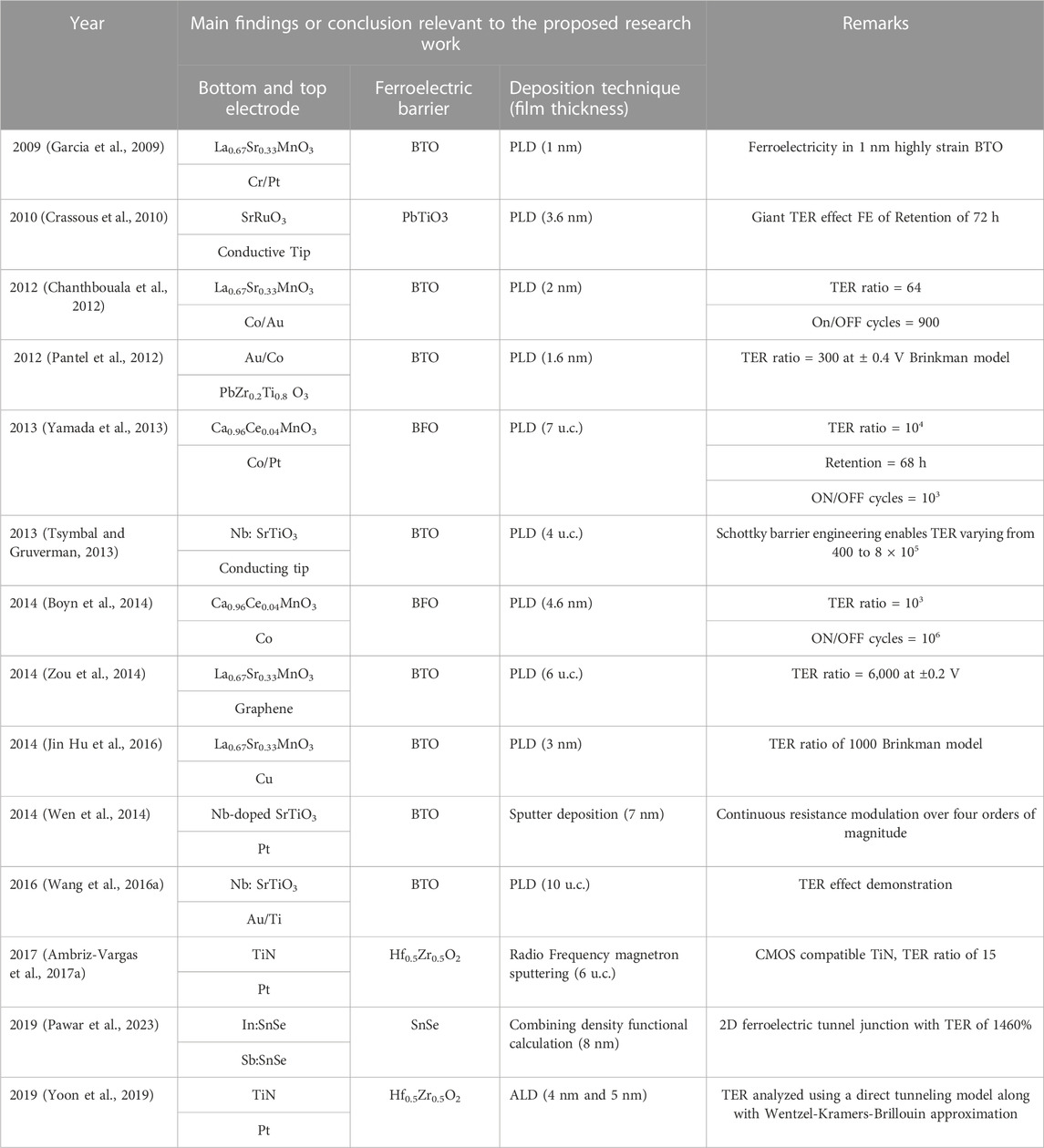
TABLE 3. The various material configuration via literature on Emerging Memories.
In a study conducted in 2013, a cobalt (Co) bottom electrode and a bismuth ferrite (BFO) barrier with a thickness of 7 unit cells were used. The results revealed a TER ratio of 104, retention of 68 h, and 103 ON/OFF cycles. By using a conducting tip on a niobium-doped strontium titanate (Nb: SrTiO3) substrate and a BTO barrier, Schottky barrier engineering was used in 2013 to generate tunable TER ratios ranging from 400 to 8 × 10⁵. The cobalt bottom electrode and a 106 ON/OFF cycle TER ratio were the main goals of the 2014 study. Cobalt as the bottom electrode and a bismuth ferrite (BFO) barrier with a thickness of 4.6 nm were employed in the 2014 study to focus on reaching a TER ratio of 103 and 106 ON/OFF cycles. The usage of graphene as a top electrode and a 6 unit cell. The BTO barrier was examined in the same year, and the results produced a high TER ratio of 6,000 at 0.2 V. As predicted by the Brinkman model, a copper top electrode and a 3 nm BTO barrier exhibited a TER ratio of 1000 in 2014. Using sputter deposition, a 7 nm thick niobium-doped strontium titanate (Nb: SrTiO3) film was deposited on a platinum (Pt) bottom electrode in 2014, enabling continuous resistance modulation over four orders of magnitude. In FTJs with a Titanium bottom electrode and a niobium-doped strontium titanate (Nb: SrTiO3) top electrode, the TER effect was proven in 2016 and the barrier had a thickness of 10 unit cells. A 2017 study used a ferroelectric barrier with a thickness of 6 u. c., a Titanium Nitride (TiN) bottom electrode, a platinum top electrode, and a hafnium zirconium oxide (Hf0.5Zr0.5O2) ferroelectric barrier to achieve a TER ratio of 15. CMOS technology was discovered to be compatible with the TiN electrode. Based on density functional calculations, a 2D ferroelectric tunnel junction using Tin Selenide (SnSe) as the barrier material and doped with indium (In) and antimony (Sb) achieved a TER of 1460% in 2019. The TER in FTJs with a TiN bottom electrode, a platinum (Pt) top electrode, and a hafnium zirconium oxide (Hf0.5Zr0.5O2) ferroelectric barrier with thicknesses of 4 nm and 5 nm were examined in another study in 2019. A direct tunnelling model and the Wentzel-Kramers-Brillouin approximation were used to analyze the TER.
3 Conclusion
The article discusses the prospect of creating a “Universal Memory” that combines the non-volatility of FLASH memory, the speed of SRAM, the great scalability of DRAM/FLASH, and the durability of DRAM/SRAM. The future of new memory technologies, including resistive RAM, magnetic RAM, phase change RAM, and ferroelectric RAM, is therefore examined. Among ferroelectric RAM, RAM based on FTJ is superior in terms of the density, retention, and speed. Since it can be produced in high density, with non-destructive read-out, and operated at high speed, FTJ, can be used to realize universal memory. If a ferroelectric material that is compatible with CMOS is found, FTJ has a lot of potential in the memory market. Non-volatile memories are still in the focus of extensive study in terms of manufacture, design, conception, and modelling.
Data availability statement
The original contributions presented in the study are included in the article/supplementary material, further inquiries can be directed to the corresponding author.
Author contributions
All authors listed have made a substantial, direct, and intellectual contribution to the work and approved it for publication.
Funding
Financial support from the Science and Engineering Research Board (SERB), Department of Science and Technology (DST), Govt. Of India for the project “CMOS compatible Ferroelectric Tunnel Junction for Universal Memory” under the Core Research Grant CRG/2018/003539 is gratefully acknowledged.
Conflict of interest
The authors declare that the research was conducted in the absence of any commercial or financial relationships that could be construed as a potential conflict of interest.
Publisher’s note
All claims expressed in this article are solely those of the authors and do not necessarily represent those of their affiliated organizations, or those of the publisher, the editors and the reviewers. Any product that may be evaluated in this article, or claim that may be made by its manufacturer, is not guaranteed or endorsed by the publisher.
References
Abdullaev, D. A., Milovanov, R. A., Volkov, R. L., Borgardt, N. I., Lantsev, A. N., Vorotilov, K. A., et al. (2020). Ferroelectric memory: state-of-the-art manufacturing and research. Russ. Technol. J. 8 (5), 44–67. doi:10.32362/2500-316x-2020-8-5-44-67
Abuwasib, M., Lee, H., Sharma, P., Eom, C.-B., Gruverman, A., and Singisetti, U. “CMOS compatible integrated ferroelectric tunnel junctions (FTJ),” in Proceedings of the 2015 73rd Annual Device Research Conference (DRC), Columbus, OH, USA, June 2015 (IEEE), 45–46.
Åkerman, J. (2005). Toward a universal memory. Sci. (80) 308 (5721), 508–510. doi:10.1126/science.1110549
Ambriz-Vargas, F., Kolhatkar, G., Broyer, M., Hadj-Youssef, A., Nouar, R., Sarkissian, A., et al. (2017a). A complementary metal oxide semiconductor process-compatible ferroelectric tunnel junction. ACS Appl. Mat. Interfaces 9 (15), 13262–13268. doi:10.1021/acsami.6b16173
Ambriz-Vargas, F., Kolhatkar, G., Thomas, R., Nouar, R., Sarkissian, A., Gomez-Yáñez, C., et al. (2017b). Tunneling electroresistance effect in a Pt/Hf0. 5Zr0. 5O2/Pt structure. Appl. Phys. Lett. 110 (9). doi:10.1063/1.4977028
Amo-Boateng, M. (2017). Super-speeds with zero-RAM: next generation large-scale optimization in your laptop!. https://arxiv.org/abs/1709.02500.
Bettinger, C. J., Ecker, M., Kozai, T. D. Y., Malliaras, G. G., Meng, E., and Voit, W. (2020). Recent advances in neural interfaces—materials chemistry to clinical translation. MRS Bull. 45 (8), 655–668. doi:10.1557/mrs.2020.195
Bez, R., and Pirovano, A. (2004). Non-volatile memory technologies: emerging concepts and new materials. Mat. Sci. Semicond. process. 7 (4–6), 349–355. doi:10.1016/j.mssp.2004.09.127
Boyn, S. (2016). Ferroelectric tunnel junctions: Memristors for neuromorphic computing. Gif-sur-Yvette, France: Université Paris-Saclay ComUE.
Boyn, S., Girod, S., Garcia, V., Fusil, S., Xavier, S., Deranlot, C., et al. (2014). High-performance ferroelectric memory based on fully patterned tunnel junctions. Appl. Phys. Lett. 104 (5). doi:10.1063/1.4864100
Cai, T., Ju, S., Wang, J., and Li, Z.-Y. (2010). “Ferroelectric and multiferroic tunnel junctions,” in Ferroelectrics (London, England: IntechOpen).
Cappelletti, P. “Non volatile memory evolution and revolution,” in Proceedings of the 2015 IEEE International Electron Devices Meeting (IEDM), Washington, DC, USA, December 2015 (IEEE), 10–11.
Chanthbouala, A., Crassous, A., Garcia, V., Bouzehouane, K., Fusil, S., Moya, X., et al. (2012). Solid-state memories based on ferroelectric tunnel junctions. Nat. Nanotechnol. 7 (2), 101–104. doi:10.1038/nnano.2011.213
Chauhan, R. N. (2007). Sonoelectrochemical synthesis of ultrafine copper deposits at ambient and sub-ambient temperatures. MTech thesis.
Chen, L., Wang, T. Y., Dai, Y. W., Cha, M. Y., Zhu, H., Sun, Q. Q., et al. (2018). Ultra-low power Hf 0.5 Zr 0.5 O 2 based ferroelectric tunnel junction synapses for hardware neural network applications. Nanoscale 10 (33), 15826–15833. doi:10.1039/c8nr04734k
Chen, W., Song, L., Wang, S., Zhang, Z., Wang, G., Hu, G., et al. (2023). Essential characteristics of memristors for neuromorphic computing. Adv. Electron. Mat. 9 (2), 2200833. doi:10.1002/aelm.202200833
Chen, Y.-F., Hsu, L.-W., Hu, C.-W., Lai, G.-T., and Wu, Y.-H. (2021). Enhanced tunneling electro-resistance ratio for ferroelectric tunnel junctions by engineering metal work function. IEEE Electron Device Lett. 43 (2), 208–211. doi:10.1109/led.2021.3133577
Cheng, C., et al. “Hf1-xZrxO2based bipolar selector with high uniformity and high selectivity for large-scale integration of memristor crossbars,” in Proceedings of the 2021 5th IEEE Electron Devices Technology and Manufacturing Conference (EDTM), Chengdu, China, April 2021 (IEEE), 1–3.
Chiou, Y. L., Gambino, J. P., and Mohammad, M. (2001). Determination of the fowler–nordheim tunneling parameters from the fowler–nordheim plot. Solid. State. Electron. 45 (10), 1787–1791. doi:10.1016/s0038-1101(01)00190-3
Crassous, A., Garcia, V., Bouzehouane, K., Fusil, S., Vlooswijk, A. H. G., Rispens, G., et al. (2010). Giant tunnel electroresistance with PbTiO 3 ferroelectric tunnel barriers. Appl. Phys. Lett. 96 (4), 10–13. doi:10.1063/1.3295700
Dörfler, A., Kolhatkar, G., Wagner, U., and Ruediger, A. (2020). The effects of thin film homogeneity on the performance of ferroelectric tunnel junctions. J. Phys. Condens. Matter 32 (18), 185302. doi:10.1088/1361-648x/ab6d15
Dubourdieu, C., Bruley, J., Arruda, T. M., Posadas, A., Jordan-Sweet, J., Frank, M. M., et al. (2013). Switching of ferroelectric polarization in epitaxial BaTiO 3 films on silicon without a conducting bottom electrode. Nat. Nanotechnol. 8 (10), 748–754. doi:10.1038/nnano.2013.192
Ezzaier, H., Marins, J. A., Claudet, C., Hemery, G., Sandre, O., and Kuzhir, P. (2018). Kinetics of aggregation and magnetic separation of multicore iron oxide nanoparticles: effect of the grafted layer thickness. Nanomaterials 8 (8), 623. doi:10.3390/nano8080623
Fabian, A.-V., Kolhatkar, G., Broyer, M., Hadj-Youssef, A., Nouar, R., Sarkissian, A., et al. (2017). A complementary metal oxide semiconductor process-compatible ferroelectric tunnel junction. ACS Appl. Mat. Interfaces 9, 13262–13268. doi:10.1021/acsami.6b16173
Fey, D., Reuben, J., and Slesazeck, S. “Comparative study of usefulness of FeFET, FTJ and ReRAM technology for ternary arithmetic,” in Proceedings of the 2021 28th IEEE International Conference on Electronics, Circuits, and Systems (ICECS), Dubai, United Arab Emirates, November 2021 (IEEE), 1–6.
Fujisaki, Y. (2013). Review of emerging new solid-state non-volatile memories. Jpn. J. Appl. Phys. 52 (4R), 040001. doi:10.7567/jjap.52.040001
Gao, P., Zhang, Z., Li, M., Ishikawa, R., Feng, B., Liu, H. J., et al. (2017). Possible absence of critical thickness and size effect in ultrathin perovskite ferroelectric films. Nat. Commun. 8 (1), 15549. doi:10.1038/ncomms15549
Gao, X. S., Liu, J. M., Au, K., and Dai, J. Y. (2012). Nanoscale ferroelectric tunnel junctions based on ultrathin BaTiO3 film and Ag nanoelectrodes. Appl. Phys. Lett. 101 (14). doi:10.1063/1.4756918
Garbin, D., Vianello, E., Bichler, O., Rafhay, Q., Gamrat, C., Ghibaudo, G., et al. (2015). HfO-Based OxRAM Devices as Synapses for Convolutional Neural Networks. IEEE Trans. Electron Devices 62 (8), 2494–2501. doi:10.1109/ted.2015.2440102
Garcia, V., and Bibes, M. (2020). Ferroelectric tunnel junctions for information storage and processing. Nat. Commun. Vol. 5, 4289. doi:10.1038/ncomms5289
Garcia, V., Fusil, S., Bouzehouane, K., Enouz-Vedrenne, S., Mathur, N. D., Barthélémy, A., et al. (2009). Giant tunnel electroresistance for non-destructive readout of ferroelectric states. Nature 460 (7251), 81–84. doi:10.1038/nature08128
Gerardin, S., and Paccagnella, A. (2010). Present and future non-volatile memories for space. IEEE Trans. Nucl. Sci. 57 (6), 3016–3039. doi:10.1109/tns.2010.2084101
Goux, L. (2019). OxRAM technology development and performances. Adv. Non-volatile Mem. Storage Technol., 3–33. doi:10.1016/B978-0-08-102584-0.00001-2
Gruverman, A., Wu, D., Lu, H., Wang, Y., Jang, H. W., Folkman, C. M., et al. (2009). Tunneling electroresistance effect in ferroelectric tunnel junctions at the nanoscale. Nano Lett. 9 (10), 3539–3543. doi:10.1021/nl901754t
Guyonnet, J., Gaponenko, I., Gariglio, S., and Paruch, P. (2011). Conduction at domain walls in insulating Pb (Zr0. 2Ti0. 8) O3 thin films. Adv. Mat. 23 (45), 5377–5382. doi:10.1002/adma.201102254
Hamdioui, S., Pouyan, P., Li, H., Wang, Y., Raychowdhur, A., and Yoon, I. “Test and reliability of emerging non-volatile memories,” in Proceedings of the 2017 IEEE 26th Asian Test Symposium (ATS), Taipei, Taiwan, November 2017 (IEEE), 175–183.
Hemavathy, B., and Meenakshi, V. “A novel design for low power Re-RAM based non-volatile flip flop using content addressable memory,” in Proceedings of the 2017 Third International Conference on Science Technology Engineering and Management (ICONSTEM), Chennai, India, March 2017, 879–883.
Huang, H.-H., et al. “A comprehensive modeling framework for ferroelectric tunnel junctions,” in Proceedings of the 2019 IEEE International Electron Devices Meeting (IEDM), San Francisco, CA, USA, December 2019, 32.
Hur, J., Park, C., Choe, G., Ravindran, P. V., Khan, A. I., and Yu, S. (2022). Characterizing HfO 2-based ferroelectric tunnel junction in cryogenic temperature. IEEE Trans. Electron Devices 69 (10), 5948–5951. doi:10.1109/ted.2022.3200919
Hwang, J., Goh, Y., and Jeon, S. (2020). Effect of insertion of dielectric layer on the performance of Hafnia ferroelectric devices. IEEE Trans. Electron Devices 68 (2), 841–845. doi:10.1109/ted.2020.3043728
Ikuno, T., Okamoto, H., Sugiyama, Y., Nakano, H., Yamada, F., and Kamiya, I. (2011). Electron transport properties of Si nanosheets: transition from direct tunneling to fowler-nordheim tunneling. Appl. Phys. Lett. 99 (2), 23107. doi:10.1063/1.3610486
Jeong, D. S., and Hwang, C. S. (2018). Nonvolatile memory materials for neuromorphic intelligent machines. Adv. Mat. 30 (42), 1704729. doi:10.1002/adma.201704729
Jeong, D. S., Thomas, R., Katiyar, R. S., Scott, J. F., Kohlstedt, H., Petraru, A., et al. (2012). Emerging memories: resistive switching mechanisms and current status. Rep. Prog. Phys. 75 (7), 076502. doi:10.1088/0034-4885/75/7/076502
Jia, C.-L., Nagarajan, V., He, J. Q., Houben, L., Zhao, T., Ramesh, R., et al. (2007). Unit-cell scale mapping of ferroelectricity and tetragonality in epitaxial ultrathin ferroelectric films. Nat. Mat. 6 (1), 64–69. doi:10.1038/nmat1808
Jin Hu, W., Wang, Z., Yu, W., and Wu, T. (2016). Optically controlled electroresistance and electrically controlled photovoltage in ferroelectric tunnel junctions. Nat. Commun. 7 (1), 10808. doi:10.1038/ncomms10808
Kim, D., Kim, J., Yun, S., Lee, J., Seo, E., and Kim, S. (2023). Ferroelectric synaptic devices based on CMOS-compatible HfAlOx for neuromorphic and reservoir computing applications. Nanoscale 15 (18), 8366–8376. doi:10.1039/d3nr01294h
Kingon, A. I., Maria, J.-P., and Streiffer, S. K. (2000). Alternative dielectrics to silicon dioxide for memory and logic devices. Nature 406 (6799), 1032–1038. doi:10.1038/35023243
Kokado, S., and Harigaya, K. (2003). A theoretical investigation of ferromagnetic tunnel junctions with 4-valued conductances. J. Phys. Condens. Matter 15 (50), 8797–8804. doi:10.1088/0953-8984/15/50/012
Kolhatkar, G., Ambriz-Vargas, F., Huber, B., Thomas, R., and Ruediger, A. (2018). Thermionic emission based resistive memory with ultrathin ferroelectric BiFe1–xCrxO3 films deposited by mineralizer-free microwave-assisted hydrothermal synthesis. Cryst. Growth Des. 18 (3), 1864–1872. doi:10.1021/acs.cgd.7b01745
Kolhatkar, G., Mittermeier, B., González, Y., Ambriz-Vargas, F., Weismueller, M., Sarkissian, A., et al. (2019). BiFe1–xCrxO3 ferroelectric tunnel junctions for neuromorphic systems. ACS Appl. Electron. Mat. 1 (6), 828–835. doi:10.1021/acsaelm.8b00111
La Torraca, P., Puglisi, F. M., Padovani, A., and Larcher, L. (2019). Multiscale modeling for application-oriented optimization of resistive random-access memory. Mater. (Basel) 12 (21), 3461. doi:10.3390/ma12213461
Lankhorst, M. H. R., Ketelaars, B. W., and Wolters, R. A. M. (2005). Low-cost and nanoscale non-volatile memory concept for future silicon chips. Nat. Mat. 4 (4), 347–352. doi:10.1038/nmat1350
Larcher, L., and Padovani, A. (2017). Multiscale modeling of oxide RRAM devices for memory applications: from material properties to device performance. J. Comput. Electron. 16 (4), 1077–1084. doi:10.1007/s10825-017-1095-3
Law, W. C., and Wong, S. D. W. (2021a). Emerging non-volatile memory technologies. Berlin, Germany: Springer.
Law, W. C., and Wong, S. D. W. (2021b). Spin transfer torque magnetoresistive random access memory. Emerg. Non-volatile Mem. Technol. Phys. Eng. Appl., 45–102.
Li, C., Huang, L., Li, T., Lü, W., Qiu, X., Huang, Z., et al. (2015). Ultrathin BaTiO3-based ferroelectric tunnel junctions through interface engineering. Nano Lett. 15 (4), 2568–2573. doi:10.1021/acs.nanolett.5b00138
Liu, L., Zhao, J., Cao, G., Zheng, S., and Yan, X. (2021). A memristor-based silicon carbide for artificial nociceptor and neuromorphic computing. Adv. Mat. Technol. 6 (12), 2100373. doi:10.1002/admt.202100373
Maksymovych, P., Jesse, S., Yu, P., Ramesh, R., Baddorf, A. P., and V Kalinin, S. (2009). Polarization control of electron tunneling into ferroelectric surfaces. Sci. (80) 324 (5933), 1421–1425. doi:10.1126/science.1171200
Marinella, M. (2014). Emerging ferroelectric memories: Critical discussion. Albuquerque, NM, United States: Sandia National Lab. SNL-NM.
Martin, J. E., Herzing, A. A., Yan, W., Li, X. q., Koel, B. E., Kiely, C. J., et al. (2008). Determination of the oxide layer thickness in core− shell zerovalent iron nanoparticles. Langmuir 24 (8), 4329–4334. doi:10.1021/la703689k
McCluskey, M. D., and Haller, E. E. (2018). Dopants and defects in semiconductors. Boca Raton, Florida, United States: CRC Press.
Mikolajick, T., Park, M. H., Begon-Lours, L., and Slesazeck, S. (2022). From ferroelectric material optimization to neuromorphic devices. Adv. Mat., 2206042. doi:10.1002/adma.202206042
Mikolajick, T., Slesazeck, S., Mulaosmanovic, H., Park, M. H., Fichtner, S., Lomenzo, P. D., et al. (2021). Next generation ferroelectric materials for semiconductor process integration and their applications. J. Appl. Phys. 129 (10). doi:10.1063/5.0037617
Mo, F., Tagawa, Y., Saraya, T., Hiramoto, T., and Kobayashi, M. “Scalability study on fcrroclcctric-HfO 2 tunnel junction memory based on non-equilibrium green function method with self-consistent potential,” in Proceedings of the 2018 IEEE International Electron Devices Meeting (IEDM), Durham, NC, USA, October 2018, 13–16.
Morozovska, A. N., Eliseev, E. A., V Morozovsky, N., and V Kalinin, S. (2017). Ferroionic states in ferroelectric thin films. Phys. Rev. B 95 (19), 195413. doi:10.1103/physrevb.95.195413
Mueller, S. “Ferroelectric HfO2 and its impact on the memory landscape,” in Proceedings of the 2018 IEEE International Memory Workshop (IMW), Kyoto, Japan, May 2018, 1–4.
Neumann, R. F., Bahiana, M., and Binggeli, N. (2013). Magnetic properties of La (0.67) Sr (0.33) MnO3/BiFeO3 (001) heterojunctions: chemically abrupt versus atomic intermixed interface. Europhys. Lett. 100.
Ogimoto, Y., Izumi, M., Sawa, A., Manako, T., Sato, H., Akoh, H., et al. (2003). Tunneling magnetoresistance above room temperature in La0. 7Sr0. 3MnO3/SrTiO3/La0. 7Sr0. 3MnO3 junctions. Jpn. J. Appl. Phys. 42 (4A), L369–L372. doi:10.1143/jjap.42.l369
Padovani, A., Larcher, L., Puglisi, F. M., and Pavan, P. “Multiscale modeling of defect-related phenomena in high-k based logic and memory devices,” in Proceedings of the 2017 IEEE 24th International Symposium on the Physical and Failure Analysis of Integrated Circuits (IPFA), Chengdu, China, July 2017 (IEEE), 1–6.
Pantel, D., Lu, H., Goetze, S., Werner, P., Jik Kim, D., Gruverman, A., et al. (2012). Tunnel electroresistance in junctions with ultrathin ferroelectric Pb (Zr0. 2Ti0. 8) O3 barriers. Appl. Phys. Lett. 100 (23). doi:10.1063/1.4726120
Park, J. Y., Lee, D. H., Park, G. H., Lee, J., Lee, Y., and Park, M. H. (2023). A perspective on the physical scaling down of hafnia-based ferroelectrics. Nanotechnology 34, 202001. doi:10.1088/1361-6528/acb945
Park, M. H., Lee, Y. H., Kim, H. J., Kim, Y. J., Moon, T., Kim, K. D., et al. (2015). Ferroelectricity and antiferroelectricity of doped thin HfO2-based films. Adv. Mat. 27 (11), 1811–1831. doi:10.1002/adma.201404531
Pawar, O. Y., Patil, S. L., Redekar, R. S., Patil, S. B., Lim, S., and Tarwal, N. L. (2023). Strategic development of piezoelectric nanogenerator and biomedical applications. Appl. Sci. 13 (5), 2891. doi:10.3390/app13052891
Pertsev, N. A., and Kohlstedt, H. (2010). Resistive switching via the converse magnetoelectric effect in ferromagnetic multilayers on ferroelectric substrates. Nanotechnology 21 (47), 475202. doi:10.1088/0957-4484/21/47/475202
Petkov, V., Ohta, T., Hou, Y., and Ren, Y. (2007). Atomic-scale structure of nanocrystals by high-energy X-ray diffraction and atomic pair distribution function Analysis: study of FexPd100-x (x = 0, 26, 28, 48) nanoparticles. J. Phys. Chem. C 111 (2), 714–720. doi:10.1021/jp066166p
Prall, K. “Scaling non-volatile memory below 30nm,” in Proceedings of the 2007 22nd IEEE Non-Volatile Semiconductor Memory Workshop, Monterey, CA, USA, August 2007 (IEEE), 5–10.
Ricci, F. (2015). Ab initio investigation of layered and low-symmetry oxides and interfaces: Multiferroic junctions, TCO’s, and a ferroelectric metal. PhD in Physics.
Richman, M. S., Li, X., and Caruso, A. N. (2019). Inadequacy of the extrapolation-length method for modeling the interface of a ferroelectric–graphene heterostructure. J. Appl. Phys. 125 (18). doi:10.1063/1.5085385
Roco, M. C., Mirkin, C. A., and Hersam, M. C. (2011). Nanotechnology research directions for societal needs in 2020: Retrospective and outlook. Berlin, Germany: Springer.
Rumberg, B., and Graham, D. W. (2013). Efficiency and reliability of Fowler-Nordheim tunnelling in CMOS floating-gate transistors. Electron. Lett. 49 (23), 1484–1486. doi:10.1049/el.2013.2401
Saitoh, M., et al. “HfO 2-based FeFET and FTJ for ferroelectric-memory centric 3D LSI towards low-power and high-density storage and AI applications,” in Proceedings of the 2020 IEEE International Electron Devices Meeting (IEDM), San Francisco, CA, USA, December 2020, 11–18.
Samara, G. A., and Morosin, B. (1973). Anharmonic effects in KTa O 3: ferroelectric mode, thermal expansion, and compressibility. Phys. Rev. B 8 (3), 1256–1264. doi:10.1103/physrevb.8.1256
Sandu, T., Tibeica, C., Nedelcu, O., Plugaru, R., and Plugaru, N. “Non-linear IV characteristics of Co/BTO/LSMO ferroelectric tunnel junction,” in Proceedings of the 2022 International Semiconductor Conference (CAS), Poiana Brasov, Romania, October 2022 (IEEE), 113–116.
Senni, S., Torres, L., Sassatelli, G., and Gamatie, A. (2016). Non-volatile processor based on MRAM for ultra-low-power IoT devices. ACM J. Emerg. Technol. Comput. Syst. 13 (2), 1–23. doi:10.1145/3001936
Sharma, U., Mishra, S., Kumar, G., and Thomas, R. (2021). 62 A universal memory that never runs out of steam. Intell. Circuits Syst., 398.
Shin, Y. “Non-volatile memory technologies for beyond 2010,” in Proceedings of the Digest of Technical Papers. 2005 Symposium on VLSI Circuits, 2005, Kyoto, Japan, June 2005 (IEEE), 156–159.
Sousa, R. C., and Prejbeanu, I. L. (2005). Non-volatile magnetic random access memories (MRAM). Comptes Rendus Phys. 6 (9), 1013–1021. doi:10.1016/j.crhy.2005.10.007
Stengel, M. (2013). Flexoelectricity from density-functional perturbation theory. Phys. Rev. B 88 (17), 174106. doi:10.1103/physrevb.88.174106
Sulaev, A., Huang, L., Li, T., Lü, W., Qiu, X., Huang, Z., et al. (2015). Ultrathin BaTiO3-based ferroelectric tunnel junctions through interface engineering. Nano Lett. 15, 2568–2573. doi:10.1021/acs.nanolett.5b00138
Suzuki, K., and Swanson, S. (2015). The non-volatile memory technology database (nvmdb). http://nvmdb.ucsd.edu.
Taherinejad, M., Vanderbilt, D., Marton, P., Stepkova, V., and Hlinka, J. (2012). Bloch-type domain walls in rhombohedral BaTiO 3. Phys. Rev. B 86 (15), 155138. doi:10.1103/physrevb.86.155138
Tsymbal, E. Y., and Gruverman, A. (2013). Beyond the barrier. Nat. Mat. 12 (7), 602–604. doi:10.1038/nmat3669
Tsymbal, E. Y., Gruverman, A., Garcia, V., Bibes, M., and Barthélémy, A. (2012). Ferroelectric and multiferroic tunnel junctions. MRS Bull. 37 (2), 138–143. doi:10.1557/mrs.2011.358
Tsymbal, E. Y., and Kohlstedt, H. (2006). Tunneling across a ferroelectric. Sci. (80) 313 (5784), 181–183. doi:10.1126/science.1126230
Tuma, T., Pantazi, A., Le Gallo, M., Sebastian, A., and Eleftheriou, E. (2016). Stochastic phase-change neurons. Nat. Nanotechnol. 11 (8), 693–699. doi:10.1038/nnano.2016.70
Useinov, A., Jagga, D., and Chang, E. Y. (2022). Tunnel electroresistance in Hf0.5Zr0.5O2-based ferroelectric tunnel junctions under hysteresis: approach of the point contact model and the linearized thomas–fermi screening. ACS Appl. Electron. Mater. 4, 2238–2245. doi:10.1021/acsaelm.2c00022
Wang, H. O., Chu, Z., Su, K. P., Tan, W. S., and Huo, D. X. (2016b). Colossal magnetoresistance of Pr0. 7Sr0. 3MnO3 layer grown on charge-ordered La0. 5Ca0. 5MnO3 manganite layer. J. Alloys Compd. 689, 69–74. doi:10.1016/j.jallcom.2016.07.165
Wang, J., Fan, Y., Song, Y., Wu, J., Zhu, R., Gao, R., et al. (2022). Microscopic physical origin of polarization induced large tunneling electroresistance in tetragonal-phase BiFeO3. Acta Mater 225, 117564. doi:10.1016/j.actamat.2021.117564
Wang, L., Cho, M. R., Shin, Y. J., Kim, J. R., Das, S., Yoon, J. G., et al. (2016a). Overcoming the fundamental barrier thickness limits of ferroelectric tunnel junctions through BaTiO3/SrTiO3 composite barriers. Nano Lett. 16 (6), 3911–3918. doi:10.1021/acs.nanolett.6b01418
Wang, P.-Z., Zhu, S.-H., Pan, T., and Wu, Y.-Z. (2015). Influence of interface within the composite barrier on the tunneling electroresistance of ferroelectric tunnel junctions with symmetric electrodes. Chin. Phys. B 24 (2), 027301. doi:10.1088/1674-1056/24/2/027301
Wang, Z. (2015). “Compact modeling and circuit design based on ferroelectric tunnel junction and spin-Hall-assisted spin-transfer torque,” in Micro and nanotechnologies/Microelectronics (Gif-sur-Yvette, France: Université Paris-Saclay ComUE).
Wang, Z. H., Zhao, W. S., Kang, W., Bouchenak-Khelladi, A., Zhang, Y., Klein, J. O., et al. (2013). Write operation study of Co/BTO/LSMO ferroelectric tunnel junction. J. Appl. Phys. 114 (4). doi:10.1063/1.4816474
Wang, Z., Wu, H., Burr, G. W., Hwang, C. S., Wang, K. L., Xia, Q., et al. (2020). Resistive switching materials for information processing. Nat. Rev. Mat. 5 (3), 173–195. doi:10.1038/s41578-019-0159-3
Wen, Z., and Wu, D. (2020). Ferroelectric tunnel junctions: modulations on the potential barrier. Adv. Mat. 32 (27), 1904123. doi:10.1002/adma.201904123
Wen, Z., Wu, D., and Li, A. (2014). Memristive behaviors in Pt/BaTiO3/Nb: srTiO3 ferroelectric tunnel junctions. Appl. Phys. Lett. 105 (5). doi:10.1063/1.4892846
Yamada, H., Garcia, V., Fusil, S., Boyn, S., Marinova, M., Gloter, A., et al. (2013). Giant electroresistance of super-tetragonal BiFeO3-based ferroelectric tunnel junctions. ACS Nano 7 (6), 5385–5390. doi:10.1021/nn401378t
Yang, E., Kim, K. R., and Chang, J. (2021). Theoretical evaluation of two-dimensional ferroelectric material CuInP 2 S 6 for ferroelectric tunnel junction device. IEEE Electron Device Lett. 42 (10), 1472–1475. doi:10.1109/led.2021.3103518
Yin, Y., Huang, W., Liu, Y., Yang, S., Dong, S., Tao, J., et al. (2015). Octonary resistance states in La0. 7Sr0. 3MnO3/BaTiO3/La0. 7Sr0. 3MnO3 multiferroic tunnel junctions. Adv. Electron. Mat. 1 (11), 1500183. doi:10.1002/aelm.201500183
Yoon, J., Hong, S., Song, Y. W., Ahn, J.-H., and Ahn, S.-E. (2019). Understanding tunneling electroresistance effect through potential profile in Pt/Hf0. 5Zr0. 5O2/TiN ferroelectric tunnel junction memory. Appl. Phys. Lett. 115 (15). doi:10.1063/1.5119948
Yuasa, S., and Djayaprawira, D. D. (2007). Giant tunnel magnetoresistance in magnetic tunnel junctions with a crystalline MgO (0 0 1) barrier. J. Phys. D. Appl. Phys. 40 (21), R337–R354. doi:10.1088/0022-3727/40/21/r01
Zenkevich, A., Minnekaev, M., Matveyev, Y., Lebedinskii, Y., Bulakh, K., Chouprik, A., et al. (2013). Electronic band alignment and electron transport in Cr/BaTiO3/Pt ferroelectric tunnel junctions. Appl. Phys. Lett. 102 (6). doi:10.1063/1.4792525
Zhao, S., Li, B., Guo, Y., and Li, H. (2022). Ferroelectric-HfO2/oxide interfaces, oxygen distribution effects, and implications for device performance. Appl. Phys. Lett. 120 (1). doi:10.1063/5.0074332
Zhuravlev, M. Y., Wang, Y., Maekawa, S., and Tsymbal, E. Y. (2009). Tunneling electroresistance in ferroelectric tunnel junctions with a composite barrier. Appl. Phys. Lett. 95 (5). doi:10.1063/1.3195075
Keywords: universal memory, ferroelectric tunnel junction, resistive switching, non-volatile (NV) memory, hafnium oxide
Citation: Sharma U, Kumar G, Mishra S and Thomas R (2023) Ferroelectric tunnel junctions: current status and future prospect as a universal memory. Front. Mater. 10:1148979. doi: 10.3389/fmats.2023.1148979
Received: 20 January 2023; Accepted: 08 September 2023;
Published: 28 September 2023.
Edited by:
Dhiren Kumar Pradhan, The University of Tennessee, Knoxville, United StatesReviewed by:
Ram Katiyar, University of Puerto Rico, Puerto RicoKB Jinesh, Indian Institute of Space Science and Technology, India
Copyright © 2023 Sharma, Kumar, Mishra and Thomas. This is an open-access article distributed under the terms of the Creative Commons Attribution License (CC BY). The use, distribution or reproduction in other forums is permitted, provided the original author(s) and the copyright owner(s) are credited and that the original publication in this journal is cited, in accordance with accepted academic practice. No use, distribution or reproduction is permitted which does not comply with these terms.
*Correspondence: Reji Thomas, cmVqaS4yMjY0OEBscHUuY28uaW4=