 Sen Wang1,2
 Lingyu Wan
95% of researchers rate our articles as excellent or good
Learn more about the work of our research integrity team to safeguard the quality of each article we publish.
Find out more
ORIGINAL RESEARCH article
Front. Mater. , 15 July 2022
Sec. Energy Materials
Volume 9 - 2022 | https://doi.org/10.3389/fmats.2022.924143
This article is part of the Research Topic Fundamental Science on Triboelectric Nanogenerators View all 5 articles
Graphene has excellent properties such as ultra-high electrical conductivity, high carrier mobility, and thermal conductivity, with a promising application in the field of triboelectric nanogenerators (TENGs). We present a systemic investigation to explore structural, optical, and temperature-dependent properties of single- and bi-layer graphene on SiC substrates, prepared by the decomposition of SiC and transferred substrate methods and their applications in TENGs. Compared to the transferred graphene onto a SiC substrate, graphene grown by the decomposition of SiC has a better crystalline quality and surface morphology, fewer impurities, and a more stress effect between graphene and the substrate. It also exhibited a longer correlation length of Raman phonons, implying better crystalline perfection. With the increase in temperature, the phonon correlation length, L, increases synchronously with TENG outputs. Among them, the TENG with a bi-layer graphene grown by the decomposition of SiC showed the best performance, especially at high temperatures. These studies provide an essential reference for further applications of graphene on SiC substrates in TENG-based devices.
Triboelectric nanogenerators (TENGs) can convert mechanical energy into electrical energy for power supply without polluting the environment (Wang, 2020; Wu et al., 2019). As an emerging distributed energy technology, TENGs are widely used in various fields such as renewable energy, electronic information, communications, and health care. To improve the performance of TENGs, materials which are prone to charge transfer are highly desirable. Monolayer graphene is an ultra-thin two-dimensional material, and the distance between C-C is about 0.142 nm (Malard et al., 2009), owning unique mechanical, electrical, and optical properties. Its excellent properties have promoted the development of electronic devices and sensor devices (Abanin et al., 2007; Balandin et al., 2008; Kane and Mele, 2005; Zhang et al., 2005), and also attract extensive attention to TENG applications.
Many TENG devices used graphene material. For example, silver nanowires (AgNWs)/redox graphene (rGO) composites were used as conductive layers to prepare a super stretch-based flexible self-powered electronic skin (e-skin) for triboelectric nanogenerators (Zhou et al., 2020). Graphene oxide (GO) nanosheets and graphene oxide nanoribbons (GONRs) were made into graphene paper as electrodes for TENGs, resulting in self-powered humidity sensors that are sensitive to water molecule adsorption (Ejehi et al., 2021). A photothermoelectric generator that integrated graphene (G) and graphene oxide (GO) composite films has been studied to make graphene-based light-driven sensors with self-powered sensing functions (Zhou et al., 2021). In addition, fibers with coated graphene were used to prepare wearable sensors that can monitor key motion during basketball and football games (Zhang et al., 2018). In these studies, graphene was mostly used as nanosheets and tiny fragments which acted as additives in other materials and then applied to TENGs as electrodes. However, graphene films that possess excellent properties are rarely explored in TENG applications. In addition, most graphene electrodes for TENG devices were studied at room temperature. But few studies revealed their temperature-dependent properties and high-temperature applications in TENGs.
Currently, graphene on SiC substrates is one of the preferred materials for the new generation of microelectronic and optoelectronic devices because of its high carrier mobility and large-scale growth prospects (W. Strupinski et al., 2011) and also a promising material in the field of TENGs. Moreover, SiC is an excellent high-temperature-resistant material for developing high-temperature devices. There is a lack of reports about the related properties of graphene on SiC substrates under variable temperature conditions and their application in TENG as an electrode layer at high temperatures. In this study, we perform a systematical investigation on the microstructure, Raman scattering spectral properties, and variable temperature properties of single- and bilayer graphene on SiC substrates prepared by both the decomposition of SiC and the transferred substrate method. By performing atomic force microscopy (AFM), scanning electronic microscopy (SEM), and X-ray photoelectron spectroscopy (XPS), the surface morphology, surface components, and covalent bond type of graphene were analyzed, and its crystal quality, impurities, and surface adsorption nature were studied. The temperature dependence of graphene was investigated by temperature-variable Raman scattering spectroscopy. Furthermore, based on the spatial correlation theory, we discussed the correlation length in the lattice and its variation with the temperature. Finally, these graphene films as an electrode layer of TENGs and their power generation performances are investigated at room temperature and at high temperatures.
Experimental samples studied in this work were prepared by the transferred graphene method and decomposition of SiC, respectively. The semi-insulation Si-face 4H-SiC wafers, about 400 μm thick, were used as substrates. The SiC-based graphene samples from the transferred graphene method were produced as follows: first, the single-layer and bilayer graphene were grown on the copper foil by the CVD method, and subsequently transferred to a 4H-SiC substrate through a standard process to obtain SiC-based graphene samples, labeled S1 and S2, respectively. From the decomposition of SiC method, 4H-SiC was used as the substrate, and the SiC (0001) surface was cleaned by chemical mechanical polishing and a standard RCA process. After H2 etching pretreatment on SiC at 1500~1600°C, the SiC (0001) surface is cleaved at a high temperature under an Ar atmosphere, and bilayer graphene was grown on the Si-terminated 4H-SiC (Si-SiC), which is marked as sample S3. The size of the experimental samples is 1 × 1 cm2.
Graphene samples were measured by AFM (Model Dimension Icon, Company BRUKER NANO INC.), SEM (Model Zeiss Sigma 500, Company Zeiss), and XPS (Model ESCALAB 250XL +, Company Thermo Fisher Scientific). Through regional surface scanning using a Dimension Icon semi-contact AFM from BRUKER NANO INC.,. Micro-region surface topography and surface roughness properties were obtained. A Zeiss Sigma 500 thermal field-emission SEM was used to measure the quality and morphology of the graphene sample. Raman spectroscopy measurements of graphene were obtained using a confocal micro-Raman spectrometer (Model LabRAM HR Evolution, Company Horiba), visualized using a ×50 objective, with the spectra recorded using 1,800 lines/mm grating. During the temperature change process, liquid nitrogen was used for temperature control and water was circulated for heat preservation in the high-temperature part. The graphene samples were all measured under the excitation of a 532 nm laser.
The micro-area surface scanning of the graphene sample was performed with an AFM, and the surface morphology and the graphene film’s surface roughness properties were obtained. Figures 1A,C,E are the AFM images of graphene samples S1, S2, and S3, respectively. Figures 1B,D,F are their SEM images. In Figure 1, the cracks can be seen at the fracture surface of the transferred graphene onto the SiC substrate, whereas the graphene grown by the decomposition of SiC is smooth, crack-free, but with a few wrinkles. The average roughness of graphene samples S1, S2, and S3 are 2.95, 2.03, and 0.443 nm, respectively.
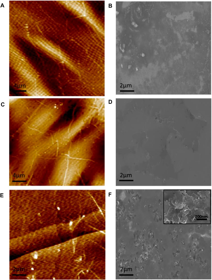
FIGURE 1. AFM and SEM images of (A,B) are for the single-layer graphene (S1) and (C,D) are for bilayer graphene (S2), both prepared by the transferred graphene. (E,F) are the AFM and SEM images of bilayer graphene (S3) prepared by the decomposition of SiC, respectively.
The surface bonding properties and atomic component analyses of the bilayer graphene prepared by both methods were examined by XPS. The XPS spectra of sample S1 are given in Supplementary Figure S1. The XPS spectra of graphene samples S2 and S3 are shown in Figure 2. Figure 2A shows the XPS spectra of the bilayer graphene in two different preparation methods, and Figures 2B–D are the O1s, Si2p, and C1s core-level spectra of graphene samples S2 and S3, respectively. It can be seen from the map that the surface of the bilayer transferred graphene onto the SiC substrate mainly contains C, O, Si, and N, whereas the surface of the bilayer graphene grown by the decomposition of SiC mainly has C, O, and Si, without N.
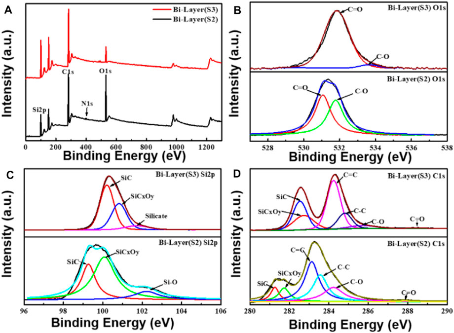
FIGURE 2. XPS electron spectra of the two types of bilayer graphene that were prepared by the substrate transfer method and the SiC pyrolysis method, respectively. (A) XPS spectra of bilayer graphene prepared by the two methods. (B–D) Spectra of O1s, Si2p, and C1s elements of the substrate-transferred bilayer graphene (S2) and SiC pyrolysis bilayer graphene (S3), respectively.
To determine the surface bonding type and elemental composition of the graphene samples, data fitting analyses were performed on the spectra of Figures 2A–C. As shown in the O1s spectra of Figure 2B, O1s is mainly contained in two chemical states of C=O/C-O, where the C=O and C-O bond binding energies of graphene sample S3 are located at 531.8 and 533.6 eV, respectively. The C=O and C-O bond binding energies of graphene sample S2 are located at 531.1 and 531.8 eV, respectively. The composition ratio of graphene sample S3 C=O/C-O is about 0.89/0.11, while the C=O bond and C-O bond of graphene sample S2 are 0.53 and 0.47, respectively. The components of the Si2p spectra in Figure 2C are associated with the SiC substrate. It is found that the intensity of the Si component at the 101.7 eV binding energy of graphene sample S3 is lower than that of the Si component at the 102.5 eV binding energy of graphene sample S2, which is due to the Si pyrolysis during the preparation of graphene by the decomposition of SiC. As seen from the C1s spectra in Figure 2D, the C1s in the two kinds of bilayer graphene mainly shows SiC (component ratio S3: 0.16, S2: 0.08), SiCxOy (component ratio S3: 0.12, S2: 0.10), C=C (component ratio S3: 0.34, S2: 0.37), C-C (component ratio S3: 0.17, S2: 0.25), C-O (component ratio S3: 0.11, S2: 0.19), and C=O (component ratio S3: 0.08, S2: 0.01) chemical states, and all show the main peak related to the 4H-SiC substrate, the G peak of the graphene and carbon interface layer, the so-called buffer layer (Hu et al., 2021). The principal peak with the binding energy of graphene sample S3 in the C1s spectrum is at 284.2 eV, and for the graphene sample S2, the principal peak with the binding energy is at 283.1 eV, both mainly contributed by the sp2 hybridization of the carbon atoms (Sheng et al., 2011). The C-O and C=O bonds’ binding energies of graphene sample S3 are located at 285.7 and 288.5 eV, respectively, and the C-O and C=O bonds’ binding energies of graphene sample S2 are located at 284.2 and 287.9 eV, respectively. The relevant results from the O1s and C1s spectra show that the substrate transfer method’s C-O and C-C bonds obtained have a higher composition ratio, indicating that the substrate transfer method still has residual solvent components during the transfer process (Ochoa-Martinez et al., 2015). In addition, according to the results of the Si2p spectrum, the components of the SiCxOy (component ratio 0.57) and the Si-O bond (component ratio 0.12) in the substrate transfer of the bilayer graphene are higher than the SiCxOy (component ratio 0.35) and the Si-O bond (component ratio 0.10) in the pyrolytic graphene, indicating that more oxygen will be adsorbed during the substrate transfer of bilayer graphene. The XPS of Figure 2 reveals different degrees of oxidation and impurity adsorption on the surfaces of both bi-layer graphene and pyrolytic graphene.
When graphene is used as the TENG electrode material, it is necessary to have a certain understanding of the relevant properties of the graphene material and the carrier concentration at room temperature, which is very important for the output characteristics of the TENG. Figures 3A,B show the room-temperature (RT) Raman spectra of the graphene samples S1, S2, and S3, respectively. Figures 3C,D correspond to the Lorentz fittings of the Raman peaks. In Figure 3A, sample S3 has a distinct second-order Raman peak of 4H-SiC in the range of 1,400 cm−1–2,000 cm−1 (Burton et al., 1999), and the Raman spectrum of 4H-SiC at room temperature is shown in Figure S2 in the Supporting Information, where the G peak’, D′ peak, partially overlaps the TO mode of substrate 4H-SiC, thus requiring a fit by the Lorentzian peak. There is also a weak band in the range of 1200–1400 cm−1. It can be signed to be the D peak of graphene for samples S1 and S2. But for sample S3, it may overlap with the spectrum of the buffer layer (F. Fromm et al., 2013), and we did not discuss this band here.
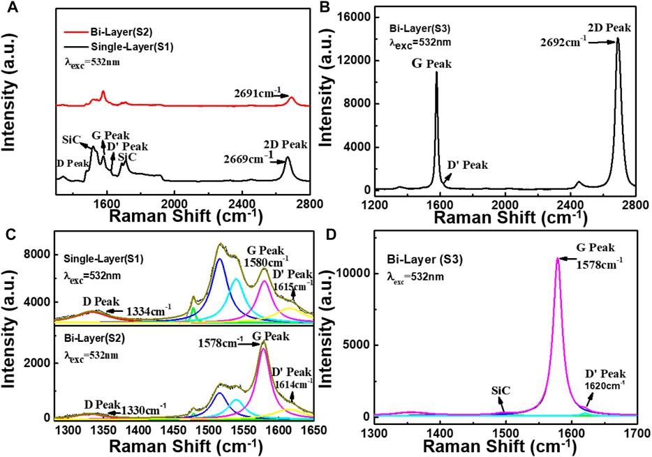
FIGURE 3. Room-temperature Raman spectra of graphene samples (S1), (S2), and (S3), respectively. (A,B) are the Raman spectra of the samples (S1), (S2), and (S3), respectively. (C,D) are the Lorentz fitting of the samples (S1), (S2), and (S3), respectively.
By the Lorentzian fit (see Figure 3C), the position of the G peak (PosS1(G)) of sample S1 is at 1580 cm−1, the full width at half maximum (FWHMS1(G)) is 28.5 cm−1, and the 2D-peak (PosS1(2D)) is at 2669 cm−1. The PosS2(G) of sample S2 is at 1578 cm−1, the FWHMS2(G) is 23.7 cm−1, and the PosS2(2D) is at 2,691 cm−1. As seen in Figure 3D, the sample S3 PosS3(G) is at 1,578 cm−1, its FWHMS3(G) is 16.4 cm−1, and PosS3 (2D) is at 2,692 cm−1. Compared with samples S1 and S2, it is worthy to note that the 2D peak of sample S3 has blue shifts of about 1 cm−1 and 23 cm−1, respectively. That would be attributed to the strong interaction between the SiC substrate and graphene. As shown in Supplementary Figure S3, we performed Raman mapping on its G peak and 2D-peak, and the results showed that sample S3 has a larger proportion of bilayer graphene.
It is well known that temperature has a certain influence on the surface charge density and the carrier mobility of electrode materials of TENGs, thereby affecting the electrical output of TENGs. The temperature characteristics such as stress-strain and carrier concentration of graphene are studied as follows. Graphene and SiC have opposite thermal expansion coefficients. Within a specific temperature range, as the temperature rises, graphene exhibits a negative thermal expansion coefficient and shrinks, whereas SiC exhibits a positive thermal expansion coefficient and expands. Therefore, graphene shrinks inward when the temperature rises, whereas the SiC substrate expands outward, and the impact of the SiC substrate on graphene possesses a tensile force. As the temperature drops, graphene expands outward, whereas the SiC substrate contracts inward, thus, the substrate acts as a compressive force on graphene.
The bidirectional variable temperature properties of graphene on the SiC substrate are studied as follows. The temperature rising range is 80–500 K and the cooling field is 300–80 K; each temperature change interval is 30 K. The Supplementary Figure S2 shows the frequency shifts of the Raman G peak of graphene samples S1, S2, and S3 as a function of bidirectional temperature. Figures 4A–D are the discrete graphs of the temperature-dependence (T-dependence) of Pos(G) and Pos(2D) of samples S1 and S2, and S3 with increasing (80–500 K) and decreasing (300–150 K) temperatures. It can be observed in Figures 4A–D that the G-peak gradually red-shifts when the temperature rises, indicating that graphene is under tensile stress, while the G-peak slowly blue-shifts as the temperature falls from room temperature (RT), indicating that graphene is under compressive stress. The Pos(G) is closely related to the sp2 carbon bond, and the C=C bond and phonon anharmonicity affect the peak shifts during the heating process (Ci et al., 2003; Burton, and Long, Feng, Ferguson., 1999). Because of the thermal expansion coefficient mismatch between the 4H-SiC substrate and graphene during the heating process from 80 to 500 K, the anharmonicity phonons will gradually dominate. Therefore, the variable temperature will lead to stress and phonon anharmonicity in graphene and the substrate (Alofi and Srivastava, 2013; Linas et al., 2015; Tian et al., 2016; Yoon et al., 2011).
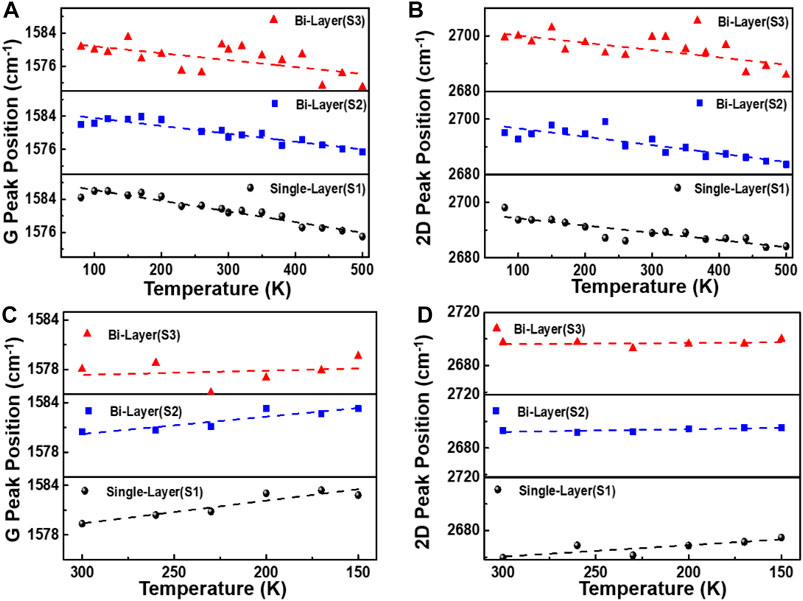
FIGURE 4. Temperature dependence of Pos (G) and Pos (2D) of samples S1, S2, and S3. (A–D) show the discrete graphs of Pos(G) and Pos(2D) of graphene prepared by different methods, cooled from room temperature to 80 K, and then heated from 80 to 500 K. Each temperature change interval is 30 K.
The temperature dependence of the G-peak Raman shift is as follows: ω = ω0+χT, where ω0 and ω are the G-peak frequency at T = 0 K and selected temperature points, respectively, and χ is the first-order temperature coefficient, which is the slope of the temperature-dependent (Han et al., 2011). From Figures 4D,F, it can be seen that when the sample was heated from 80–500 K, the Pos(G) of the sample S1 is as follows: χ = −(2.57 ± 0.18)×10−2 cm−1/K, and for sample S2, it is χ = −(1.89 ± 0.20)×10−2 cm−1/K, while for sample S3, it is χ = −(1.66 ± 0.52)×10−2 cm−1/K. On the contrary, when the sample was cooled down to 80 K, the Pos(G) for sample S1 is χ = −(2.76 ± 0.53)×10−2 cm−1/K, and for sample S2, it is χ = −(2.10 ± 0.50)×10−2 cm−1/K, while for sample S3, it is χ = −(0.52 ± 1.34)×10−2 cm−1/K. The large variation of Pos(G) in bilayer graphene grown by the decomposition of SiC with temperature change is related to graphene defects, carrier concentration, and non-uniform number of layers (F. Ejehi et al., 2021).
Since graphene on 4H-SiC does not grow as a simple AB stack but a high-density rotating fault stack, the decomposition-grown multi-layer graphene on SiC possesses an indistinguishable electronic structure from single-layer graphene in the vicinity of the Dirac point (Wu et al., 2018). Therefore, the 2D-peak is fitted as a single Lorentz peak. Intriguingly, the 2D-peak is a double resonance (DR) process, and it exhibits a strong dependence on the band structure. As the temperature is changed, the band structure of graphene will vary with temperature, so the 2D-peak will also shift (Liu et al., 2019). Figures 5A–C are an analysis of the FWHM (G) and FWHM (2D). As shown in Figure 5A, the FWHM (G) of graphene obtained by the two different preparation methods fluctuates only in a small range no matter if the temperature increases or decreases, indicating that the graphene FWHM (G) is not sensitive to temperature changes. The FWHM (2D) of graphene samples S1 and S2 in Figure 5B fluctuate to a certain extent in the temperature range of 80–300 K, but the fluctuation range is not extensive. However, after 300 K, the FWHM (2D) of samples S1 and S2 gradually increases when the temperature rises.
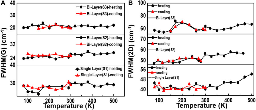
FIGURE 5. FWHM changes for different samples during temperature changes. (A) Change of FWHM of the G peak during the heating and cooling process. (B) FWHM (2D) of single- and bilayer graphene with two growth ways as a function of temperature.
The Raman scattering spectrum includes the scattering intensity, Raman frequency shift, and FWHM of its phonon mode spectrum. Since doping or lattice disorder will destroy the integrity of the lattice, there is a certain degree of shift or FWHM change in the Raman peak. Therefore, the microstructure and crystallization properties of graphene crystals can be analyzed by studying the spatial correlation theoretical model of Raman spectrum lines. Based on the spatial correlation theory, the first-order Raman scattering peak G of graphene can be quantitatively analyzed. The phonon correlation length L is used to measure the average distance between point defects (Ferreira et al., 2010) to describe the crystal quality (Havel et al., 2004). The intensity of the first-order Raman spectrum I(ω) can be deduced from the spatial correlation model of the Gaussian distribution function as (Chuan, 2000; Ferreira et al., 2010; Havel et al., 2004; Chen et al., 2017):
where q is expressed in units of
with A and B as adjustable parameters, A is the Lorentz fitting peak position value according to the experimental data, and B is the peak position fitting calibration value. Combining the spatial correlation model formula Eq. 1 and formula Eq. 2, the Raman spectrum of the graphene sample is fitted and analyzed, and the fitting results are shown in Table 1. The analysis shows that the G-peak of sample S3 has the longest correlation length, indicating that its lattice integrity is the best.
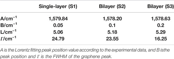
TABLE 1. Theoretical fitting parameters of the Raman mode excited at 532 nm for the three samples at room temperature.
The verification analysis of the change in defects in graphene samples during the temperature change process was carried out. According to the spatial correlation theory, the variation of the Raman spectral feature G-peak phonon correlation length with temperature is obtained by a fitting analysis, as shown in Figures 6A–C it is clearly shown that as the temperature rises, the correlation length L gradually increases, implying better crystalline perfection.
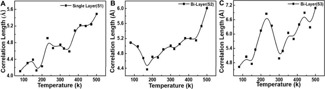
FIGURE 6. (A–C) Variation of the G-peak phonon propagation length with increasing temperature.
Based on the aforementioned analysis of graphene materials, we found that graphene has more excellent properties at high temperatures and it will be a good candidate for TENG applications. As shown in Figure 7A, transferred bilayer graphene (S2), the graphene grown by the decomposition of SiC (S3), and CVD growth of monolayer graphene on a copper foil were applied in TENGs as electrode layers while the PTFE films are used as the other friction layers. Among them, the area of TENGs designed by S2 and S3 is both 1 cm × 1 cm, and the area of TENGs designed by the CVD growth of monolayer graphene on the copper foil is 2 cm × 2 cm, as shown in Supplementary Figure S5. On the principle of the combination of contact electrification and electrostatic induction, Figure 7B shows a schematic diagram of the working principle of TENGs.
FIGURE 7. Principles and output tests of three different TENGs. (A) Schematic diagrams showing the working principle of the TENG. (B) Contact electrification mechanism of TENGs. (C) Qsc of the Cu-TENG and C-TENG at room temperature. (D,E) Histograms of Voc, Isc, and Qsc measured during the temperature rise from 373 to 473 K for the T-TENG, D-TENG, and C-TENG in a 1 cm × 1 cm area. (F,G) are the transferred charges of the C-TENG and Cu-TENG under the same conditions, respectively. (H) Histograms of Qsc for the C-TENG and Cu-TENG from 373 to 473 K with an area of 2 cm × 2 cm.
We compared the TENG made from bilayer graphene grown by SiC decomposition (D-TENG), the TENG made from transferred bilayer graphene (T-TENG), and the TENG designed by the CVD growth of monolayer graphene on the copper foil (C-TENG) (area 1 cm × 1 cm). Figure 7C is the charge transfer (Qsc) of three TENGs at room temperature. D-TENG had the highest Qsc of about 0.71 nC and C-TENG had the lowest Qsc of about 0.30 nC. The results of a short-circuit current (Isc) and an open-circuit voltage (Voc) for the three TENGs at room temperature are shown in Supplementary Figure S6. The results show that D-TENG has the best output performance. It has been shown that van der Waals forces exist between graphene layers; hence, the in-plane conductivity of transferred graphene is better than the out-of-plane conductivity. In contrast, graphene grown by decomposing SiC has a three-dimensional structure with seamless connections between the layers, which makes graphene with good out-of-plane conductivity while maintaining good in-plane conductivity (Xue et al., 2015). Therefore, D-TENG has the best output performance compared with the other two TENGs. Supplementary Figure S7 shows the output results for the three TENG temperatures from 293 K up to 373 K. From the results, we can see that the output does not change much in this temperature range. Therefore, to better understand the effect of graphene on TENGs at variable temperatures, we gradually ramp up the temperature from 373 to 473 K to compare the outputs of the three TENGs. Figures 7D,E show histograms of the variation of Voc and Qsc over the temperature range 373–473 K for the three TENGs, respectively. Histograms of the variation of Isc with temperature are shown in Supplementary Figure S8. It was observed that the outputs of T-TENG and C-TENG increase steadily with increasing temperature, and the output of D-TENG fluctuates with the temperature. Among the three TENGs, D-TENG exhibits the best performance. As shown in Supplementary Figure S9, the transferred charges between the Cu electrode and the zero potential increased with the increase in temperature. This means that at high temperatures, more charges transferred between the PTFE surface and the Cu electrode in the contact-separation process. The electrons on the PTFE surface are thermally emitted (Xu et al., 2018a; Xu et al., 2018b) which indicates that the copper rapidly replenished the electrons to the PTFE surface in contact. Meanwhile, the conductivity of graphene improves with increasing temperature, thus contributing to a constant and steady increase in the outputs of TENGs.
We also compared the properties of charge transfer in TENGs with and without graphene at variable temperatures. At room temperature, we performed 180 contact-separation cycles on TENGs fabricated with copper as the electrode (Cu-TENG) and the C-TENG under the same experimental condition and their transferred charges are shown in Figures 7F,G. The C-TENG had a faster and higher charge transfer than the Cu-TENG, with a transfer charge of 1.12 nC. It may be related to the existence of defects in graphene such as holes (Guo et al., 2014), which will trap electrons. These electrons cannot move freely, graphene is negative (Zou et al., 2020), and therefore the transfer charge of the C-TENG will be higher. The Isc and Voc for both TENGs are given in Supplementary Figure S10. Figure 7H shows the changes of Qsc for the Cu-TENG and C-TENG during the temperature increase from 373 to 473 K, respectively. The change of Voc and Isc during the temperature increase from 373 to 473 K for the Cu-TENG and C-TENG is shown in Supplementary Figure S11. The TENG with graphene as the electrode outperforms the TENG with the copper electrode, and the output of the TENG with graphene as the electrode increases steadily with the increase in temperature. This result may be because of a combination of improved electrical conductivity and electronegativity. Based on the aforementioned analysis, we can conclude that graphene as the electrode in the TENG can achieve better TENG output at higher temperatures.
In this study, single- and bilayer graphene prepared by the substrate transfer method and bilayer graphene grown by the decomposition of SiC, were studied for film quality, surface composition, stress–strain, and temperature-dependent properties. The results show some differences in the peak position, FWHM, and temperature-dependent features of the G peak and 2D peak between graphene growth by the decomposition of SiC and transferred graphene. Moreover, graphene grown by the decomposition of SiC has fewer impurities, better surface morphology, crystalline quality, and temperature stability. Based on the spatial correlation theory, it is found that the correlation length L of the G-peak phonons tends to increase simultaneously with the increase in temperature. The comparison results of the Cu-TENG and the C-TENG show that graphene and PTFE exchange electrons more easily. By comparing the output of the D-TENG, T-TENG, and C-TENG at variable temperatures, the results showed that graphene as an electrode can achieve better TENG performance at higher temperatures. We have conducted an in-depth temperature-dependent exploration of graphene, which is beneficial to the high-temperature application in the field of TENGs.
The original contributions presented in the study are included in the article/Supplementary Material; further inquiries can be directed to the corresponding authors.
SW: methodology, investigation, data curation, and writing—original draft. LW: methodology, investigation, writing—review and editing, and funding acquisition. DL: supervision and validation. XC: resources and supervision. XX: resources and supervision. ZF: supervision, validation, and writing—review and editing. IF: supervision and validation.
This work was supported by the National Key R and D Project from Minister of Science and Technology (2021YFA1201603) and the Guangxi Natural Science Foundation, China (2018GXNS–FAA138127).
The authors declare that the research was conducted in the absence of any commercial or financial relationships that could be construed as a potential conflict of interest.
All claims expressed in this article are solely those of the authors and do not necessarily represent those of their affiliated organizations, or those of the publisher, the editors, and the reviewers. Any product that may be evaluated in this article, or claim that may be made by its manufacturer, is not guaranteed or endorsed by the publisher.
The Supplementary Material for this article can be found online at: https://www.frontiersin.org/articles/10.3389/fmats.2022.924143/full#supplementary-material
Abanin, D. A., Lee, P. A., and Levitov, L. S. (2007). Randomness-InducedXYOrdering in a Graphene Quantum Hall Ferromagnet. Phys. Rev. Lett. 98 (15), 156801. doi:10.1103/PhysRevLett.98.156801
Alofi, A., and Srivastava, G. P. (2013). Thermal Conductivity of Graphene and Graphite. Phys. Rev. B 87 (11). doi:10.1103/PhysRevB.87.115421
Balandin, A. A., Ghosh, S., Bao, W., Calizo, I., Teweldebrhan, D., Miao, F., et al. (2008). Superior Thermal Conductivity of Single-Layer Graphene. Nano Lett. 8 (3), 902–907. doi:10.1021/nl0731872
Burton, J. C., Sun, L., Feng, Z. C., and Ferguson, I. T. (1999). First- and Second-Order Raman Scattering from Semi-insulating4H−SiC. Phys. Rev. B 59, 7282–7284. doi:10.1103/PhysRevB.59.7282
Chen, S., Wan, L., Xie, D., Qiu, Z. R., Jiang, X., Tin, C.-C., et al. (2017). Adducing Crystalline Features from Raman Scattering Studies of Cubic SiC Using Different Excitation Wavelengths. J. Phys. D. Appl. Phys. 50, 115102. doi:10.1088/1361-6463/aa5626
Chuan, F. Z. (2000). “Micro-Raman Scattering and Micro-photoluminescence on GaN Materials Grown on Sapphire by Metalorganic Chemical Vapor Deposition,” in Optical Devices and Diagnostics in Materials Science. Editors D. L. Andrews, T. Asakura, S. Jutamulia, W. P. Kirk, M. G. Lagally, and R. B. Lal, SPIE(Optical Eengineerin), 41, 2022.
Ci, L., Zhou, Z., Song, L., Yan, X., Liu, D., Yuan, H., et al. (2003). Temperature Dependence of Resonant Raman Scattering in Double-Wall Carbon Nanotubes. Appl. Phys. Lett. 82 (18), 3098–3100. doi:10.1063/1.1572959
Ejehi, F., Mohammadpour, R., Asadian, E., Fardindoost, S., and Sasanpour, P. (2021). Enhancement of Self-Powered Humidity Sensing of Graphene Oxide-Based Triboelectric Nanogenerators by Addition of Graphene Oxide Nanoribbons. Microchim. Acta 188 (8), 251. doi:10.1007/s00604-021-04921-y
Fromm, F., Oliveira Jr, M. H., Molina-Sánchez, A., Hundhausen, M., Lopes, J. M. J., Riechert, H., et al. (2013). Contribution of the Buffer Layer to the Raman Spectrum of Epitaxial Graphene on SiC(0001). New J. Phys. 15, 043031. doi:10.1088/1367-2630/15/4/043031
Guo, Y., Guo, L. W., Huang, J., Yang, R., Jia, Y. P., Lin, J. J., et al. (2014). The Correlation of Epitaxial Graphene Properties and Morphology of SiC (0001). J. Appl. Phys. 115 (4), 043527. doi:10.1063/1.4863796
Han, R., Han, B., Wang, D. H., and Li, C. (2011). Temperature Dependence of Raman Scattering from 4H-SiC with Hexagonal Defects. Appl. Phys. Lett. 99 (1), 011912. doi:10.1063/1.3609009
Havel, M., Baron, D., and Colomban, P. (2004). 'Smart' Raman/Rayleigh Imaging of Nanosized SiC Materials Using the Spatial Correlation Model. J. Mater. Sci. 39 (20), 6183–6190. doi:10.1023/B:JMSC.0000043585.29016.5a
Hu, T., Yang, D., Hu, W., Xia, Q., Ma, F., and Xu, K. (2021). The Structure and Mechanism of Large-Scale Indium-Intercalated Graphene Transferred from SiC Buffer Layer. Carbon 171, 829–836. doi:10.1016/j.carbon.2020.09.055
Kane, C. L., and Mele, E. J. (2005). Quantum Spin Hall Effect in Graphene. Phys. Rev. Lett. 95 (22), 226801. doi:10.1103/PhysRevLett.95.226801
Linas, S., Magnin, Y., Poinsot, B., Boisron, O., Förster, G. D., Martinez, V., et al. (2015). Interplay between Raman Shift and Thermal Expansion in Graphene: Temperature-dependent Measurements and Analysis of Substrate Corrections. Phys. Rev. B 91 (7), 075426. doi:10.1103/PhysRevB.91.075426
Liu, H.-N., Cong, X., Lin, M.-L., and Tan, P.-H. (2019). The Intrinsic Temperature-dependent Raman Spectra of Graphite in the Temperature Range from 4K to 1000K. Carbon 152, 451–458. doi:10.1016/j.carbon.2019.05.016
Malard, L. M., Pimenta, M. A., Dresselhaus, G., and Dresselhaus, M. S. (2009). Raman Spectroscopy in Graphene. Phys. Rep. 473 (5), 51–87. doi:10.1016/j.physrep.2009.02.003
Martins Ferreira, E. H., Moutinho, M. V. O., Stavale, F., Lucchese, M. M., Capaz, R. B., Achete, C. A., et al. (2010). Evolution of the Raman Spectra from Single-, Few-, and Many-Layer Graphene with Increasing Disorder. Phys. Rev. B 82 (12), 9. doi:10.1103/PhysRevB.82.125429
Ochoa-Martínez, E., Gabás, M., Barrutia, L., Pesquera, A., Centeno, A., Palanco, S., et al. (2015). Determination of a Refractive Index and an Extinction Coefficient of Standard Production of CVD-Graphene. Nanoscale 7 (4), 1491–1500. doi:10.1039/c4nr06119e
Sheng, Z.-H., Shao, L., Chen, J.-J., Bao, W.-J., Wang, F.-B., and Xia, X.-H. (2011). Catalyst-Free Synthesis of Nitrogen-Doped Graphene via Thermal Annealing Graphite Oxide with Melamine and its Excellent Electrocatalysis. Acs Nano 5 (6), 4350–4358. doi:10.1021/nn103584t
Strupinski, W., Grodecki, K., Wysmolek, A., Stepniewski, R., Szkopek, T., Gaskell, P. E., et al. (2011). Graphene Epitaxy by Chemical Vapor Deposition on SiC. Nano Lett. 11 (4), 1786–1791. doi:10.1021/nl200390e
Tian, S., Yang, Y., Liu, Z., Wang, C., Pan, R., Gu, C., et al. (2016). Temperature-dependent Raman Investigation on Suspended Graphene: Contribution from Thermal Expansion Coefficient Mismatch between Graphene and Substrate. Carbon 104, 27–32. doi:10.1016/j.carbon.2016.03.046
Wang, Z. L. (2020). Triboelectric Nanogenerator (TENG)-Sparking an Energy and Sensor Revolution. Adv. Energy Mat. 10 (17), 2000137. doi:10.1002/aenm.202000137
Wu, C., Wang, A. C., Ding, W., Guo, H., and Wang, Z. L. (2019). Triboelectric Nanogenerator: A Foundation of the Energy for the New Era. Adv. Energy Mat. 9 (1), 1802906. doi:10.1002/aenm.201802906
Wu, J.-B., Lin, M.-L., Cong, X., Liu, H.-N., and Tan, P.-H. (2018). Raman Spectroscopy of Graphene-Based Materials and its Applications in Related Devices. Chem. Soc. Rev. 47 (5), 1822–1873. doi:10.1039/c6cs00915h
Xu, C., Wang, A. C., Zou, H., Zhang, B., Zhang, C., Zi, Y., et al. (2018a). Raising the Working Temperature of a Triboelectric Nanogenerator by Quenching Down Electron Thermionic Emission in Contact-Electrification. Adv. Mat. 30 (38), 1803968. doi:10.1002/adma.201803968
Xu, C., Zi, Y., Wang, A. C., Zou, H., Dai, Y., He, X., et al. (2018b). On the Electron-Transfer Mechanism in the Contact-Electrification Effect. Adv. Mat. 30 (15), 1706790. doi:10.1002/adma.201706790
Xue, Y., Ding, Y., Niu, J., Xia, Z., Roy, A., Chen, H., et al. (2015). Rationally Designed Graphene-Nanotube 3D Architectures with a Seamless Nodal Junction for Efficient Energy Conversion and Storage. Sci. Adv. 1 (8), e1400198. doi:10.1126/sciadv.1400198
Yoon, D., Son, Y.-W., and Cheong, H. (2011). Negative Thermal Expansion Coefficient of Graphene Measured by Raman Spectroscopy. Nano Lett. 11 (8), 3227–3231. doi:10.1021/nl201488g
Zhang, J., Cao, Y., Qiao, M., Ai, L., Sun, K., Mi, Q., et al. (2018). Human Motion Monitoring in Sports Using Wearable Graphene-Coated Fiber Sensors. Sensors Actuators A Phys. 274, 132–140. doi:10.1016/j.sna.2018.03.011
Zhang, Y., Tan, Y.-W., Stormer, H. L., and Kim, P. (2005). Experimental Observation of the Quantum Hall Effect and Berry's Phase in Graphene. Nature 438 (7065), 201–204. doi:10.1038/nature04235
Zhou, K., Zhao, Y., Sun, X., Yuan, Z., Zheng, G., Dai, K., et al. (2020). Ultra-stretchable Triboelectric Nanogenerator as High-Sensitive and Self-Powered Electronic Skins for Energy Harvesting and Tactile Sensing. Nano Energy 70, 104546. doi:10.1016/j.nanoen.2020.104546
Zhou, P., Lin, J., Zhang, W., Luo, Z., and Chen, L. (2021). Photo-thermoelectric Generator Integrated in Graphene-Based Actuator for Self-Powered Sensing Function. Nano Res. 15, 5376–5383. doi:10.1007/s12274-021-3791-3
Keywords: triboelectric nanogenerators, SiC-based graphene, spatial correlation theory, carrier concentration, temperature-dependent properties
Citation: Wang S, Wan L, Li D, Chen X, Xu X, Feng ZC and Ferguson IT (2022) Temperature-Dependent Properties of Graphene on SiC Substrates for Triboelectric Nanogenerators. Front. Mater. 9:924143. doi: 10.3389/fmats.2022.924143
Received: 20 April 2022; Accepted: 06 June 2022;
Published: 15 July 2022.
Edited by:
Sihong Wang, The University of Chicago, United StatesReviewed by:
Ivan Shtepliuk, Linköping University, SwedenCopyright © 2022 Wang, Wan, Li, Chen, Xu, Feng and Ferguson. This is an open-access article distributed under the terms of the Creative Commons Attribution License (CC BY). The use, distribution or reproduction in other forums is permitted, provided the original author(s) and the copyright owner(s) are credited and that the original publication in this journal is cited, in accordance with accepted academic practice. No use, distribution or reproduction is permitted which does not comply with these terms.
*Correspondence: Lingyu Wan, bHl3MjAxN0BneHUuZWR1LmNu; Zhe Chuan Feng, emNmZW5nQG50dS5lZHUudHc=
Disclaimer: All claims expressed in this article are solely those of the authors and do not necessarily represent those of their affiliated organizations, or those of the publisher, the editors and the reviewers. Any product that may be evaluated in this article or claim that may be made by its manufacturer is not guaranteed or endorsed by the publisher.
Research integrity at Frontiers
Learn more about the work of our research integrity team to safeguard the quality of each article we publish.