 He Wang
 Xiangkun Kong
 Xinyu Zhang
95% of researchers rate our articles as excellent or good
Learn more about the work of our research integrity team to safeguard the quality of each article we publish.
Find out more
ORIGINAL RESEARCH article
Front. Mater. , 20 June 2022
Sec. Metamaterials
Volume 9 - 2022 | https://doi.org/10.3389/fmats.2022.912913
This article is part of the Research Topic Multifunctional and Reconfigurable Electromagnetic and Acoustic Metasurfaces View all 9 articles
This study proposes a dual-polarized frequency-selective rasorber (FSR) with a switchable wide passband. The FSR is made up of two layers: the first is a lossy frequency-selective surface (FSS), which is made up of meander lines and lumped resistors that absorb energy. The position of the lumped resistors can be determined via characteristic mode analysis. Another layer is a lossless FSS with PIN diodes for the reconfigurable function. The lossless FSS is made up of three layers for a wide passband. When PIN diodes are turned off, the absorption bands in the lower band vary from 2.73 to 3.76GHz, while the upper band ranges from 6.07 to 7.94 GHz. Meanwhile, the reflect band with a value greater than −3 dB spans the frequency range from 4.21 to 5.88 GHz. When the PIN diodes are turned on, the passband with insertion loss less than −1 dB extends from 3.82 to 5.3 GHz. At the same time, the absorption band ranges from 5.9 to 7 GHz. Due to the nonlinearity of PIN diodes, there is a certain difference between the simulated and the measured results. Also, we analyzed the influence of the inductance value of PIN diodes on the whole structure.
FSR is a device that transmits waves in the working band and absorbs waves out of the working band. Because of its spatial filtering characteristics, it has received extensive attention in recent years, so it is usually used to design a radome because it can realize the antenna in-band transceiver function, and at the same time, the stealth function is realized outside the working band of the antenna, which greatly reduces the RCS of the antenna.
In most literature works, the FSR is usually a two-layer structure, a lossy layer and a lossless layer, and the passband frequency of the lossy layer and the lossless layer are the same. When designing an FSR, the method of equivalent circuit is usually used to fit the simulation results so as to adjust the frequency by changing the parameters of the structure. Some studies have proposed a method for mapping the equivalent circuit’s lumped element to the geometric size of FSS (Shang et al., 2013). However, some advanced theories can also be applied to the analysis and design of antennas and FSS. Garbacz (1965) first proposed the characteristic mode theory (CMT) in 1965 and pointed out that CMT can perform the mode analysis of metal targets with an arbitrary shape. Before the 1990s, the application of CMT mostly focused on scattering control, pattern synthesis, and antenna shape synthesis (Shi et al., 2019; Elias et al., 2021; Shi et al., 2021). Since the 1990s, the application and development of CMT have been focusing on antenna engineering and have become one of the mainstream choices for the antenna system analysis and design. It can provide a clearer physical insight into radiation behavior compared to the equivalent circuit method (Vogel et al., 2015; Zha et al., 2021). In recent years, some articles try to analyze absorbers by using CMT (Guo et al., 2020; Wu et al., 2021).
The lossy layer is often composed of metal meander lines and lumped resistors (Shang et al., 2014a; Wang et al., 2020). Meanwhile, resistive ink is sometimes used for designing the lossy layer in some literature (Costa and Monorchio, 2012). In recent years, a three-dimensional (3D) FSR has also been proposed (Yu Y. et al., 2019). The structure of the FSR is more complicated than the multilayered structure, but it has great selectivity and angular stability (Yu W. et al., 2019). In addition, with the development of wireless communication, the development of reconfigurable FSR has gradually attracted attention. At present, there are many reconfigurable methods, such as the use of mechanics, optics, and liquid state, but in contrast, electronic control is the most efficient method, which is also more suitable for wireless communication systems. The reconfigurable FSR can create a switchable rasorber with a passband, which can be shifted into an absorption band to produce in-band stealth performance when the FSR is utilized as a radome (Chen et al., 2017; Li et al., 2020; Li et al., 2021; Yuan et al., 2021; Zhu et al., 2021). The switchable function of reconfigurable FSRs is often achieved by PIN diodes.
By far, the passband of the reconfigurable FSR mentinoned before is not wide enough to match a wide-band antenna. In this work, we design a lossy FSS by using characteristic mode analysis. Also, a three-layer lossless FSS with PIN diodes is proposed to broaden the passband. Then, we cascade the lossy FSS and lossless FSS to build a reconfigurable FSR, which can provide a wide passband when the PIN diodes are operating and a reflect band when the PIN diodes are turned off.
The basic assumption of the characteristic mode theory (CMT) is that the scattering or radiation mode of any object is a linear combination of its modes. Characteristic modes are decided by the shape of the metal object and excited by the incident field (the object acts as a scatter).
The characteristic mode theory is based on the moment method (MOM) and whose eigenequations are:
It is not easy to observe because the rank of
As the
A typical FSR can be modeled with a two-port network according to Shang et al. (2014b), as shown in Figure 1.
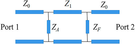
FIGURE 1. Two-port network of FSR.
For the ideal FSR, |S11| = 0 and |S21| = 0 at the absorption band, and |S21| = 1 and |S11| = 0 at the passband. However, in the practical FSR design, the absorption rate (AR) in the absorption band is usually not less than 80%, and the insertion loss is less than 3dB at the passband. The absorption rate of FSR is defined as follows:
To simplify the impedance conditions of a lossy FSS, we assume that
In the FSR design, we usually consider S11 and S21 less than −10dB as the absorbing condition. Therefore, we can deduce the value range of RA and XA when S11 is less than −10dB from the formula of Eq. 6. Figure 2 clearly shows the cover of RA and XA during the absorption band. The purple and green parts represent the real and imaginary ranges of ZA, respectively.
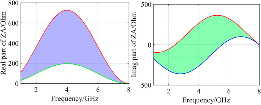
FIGURE 2. Impedance range of ZA at the absorptive band with S11 < −10dB and S21 < −10 dB.
To design a lossy FSS, we replace the lossless FSS with a ground plane. The lossy FSS is designed by using a metal meander line and lumped resistors which is similar to the structure in Shang et al. (2014b). The structure of the absorber is shown in Figure 3, in which the blue part represents the dielectric layer whose dielectric constant is 2.2. The purple part is the air gap with a thickness h2=15 mm. The dimensions of the lossy FSS are l1 = 14mm, l2 = 3.2mm, l3 = 4mm, l4 = 6.2mm, w1 = 0.3mm, s1 = 0.2mm, and h1 = 0.5 mm.
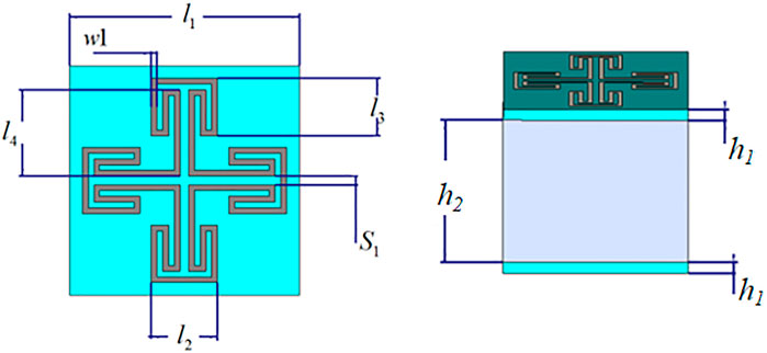
FIGURE 3. Structure of the lossy FSS.
To absorb the incident wave, some lumped resistors should be inserted into the structure. The position and the value of lumped resistors are chosen by using characteristic mode analysis. In this study, the mode significance (MS) shown in Figure 4 is obtained by using CST Studio Suite 2019. Mode 4 and mode 5 are invalid modes because their mode significance is too small to be excited.
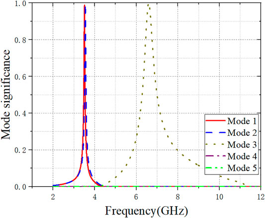
FIGURE 4. Mode significance of the meander line.
Figure 5A shows the mode fields of modes at their respective resonant frequencies. Mode 1, mode 2, and mode 3 are effective modes for normal incidence because the main lobes of mode 1, mode 2, and mode 3 are normal to the unit cell.
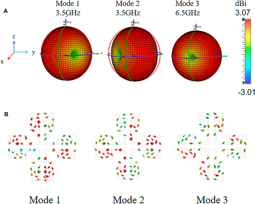
FIGURE 5. (A) Mode fields of the modes. (B) Characteristic current of resonant frequencies.
As shown in Figure 5B, the red part represents the high characteristic current when the incident wave is arriving. To absorb the energy, we then put the lumped resistors where the characteristic current is high. The structure and S-parameter of the lossy layer are shown in Figure 6A. There is a passband at around 4.2 GHz. We can determine the position of the absorption band through the impedance of the lossy layer, as shown in Figures 6B,C. It can be seen that if the lossless layer is a metal plate, its absorption bands are in the range of 1.5–3 GHz and 5.3–6.8 GHz.
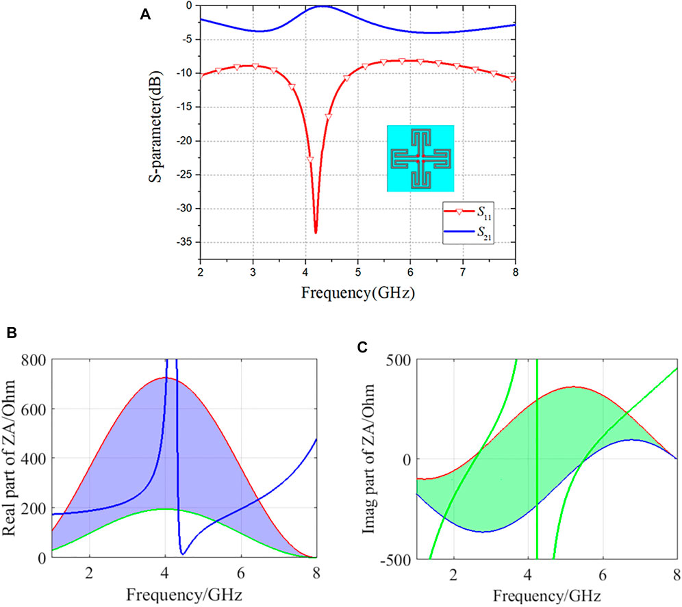
FIGURE 6. (A) Structure and S-parameter of the lossy FSS. (B) Real part of the impedance. (C) Imaginary part of the impedance.
To expand the bandwidth of the passband, the lossless layer is designed by a multilayer-coupled FSS, whose structure is shown in Figure 7.

FIGURE 7. Structure of the lossless FSS.
The dimensions of the lossless FSS are: p = 14mm, l5 = 11mm, t = 3.2mm, m = 3mm, and w1 = 4.5 mm. The black part is a PIN diode that is chosen to achieve a switchable function. The PIN diode is modeled according to its data sheet where a small resistance Rpin = 1.05Ω is connected in series with an inductance Lpin = 1.5nH in the ON state. Meanwhile, a capacitance Cpin = 0.15pF connected in series with Lpin during the OFF state is considered. When PIN diodes are turned on, the principle is the same as that of the coupled FSS. When PIN diodes are turned off, the structure of the coupled FSS is destroyed, resulting in a reflection effect. In addition, the equivalent circuit of lossless FSS is given in Figure 8A. The circuit simulation is conducted with following optimized values: L1 = 0.501nH, C1 = 0.125pF, L2 = 20nH, C2 = 38.06pF, L3 = 3.1nH, C3 = 0.08pF, and C4 = 0.98pF.
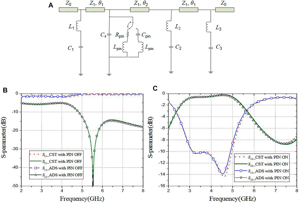
FIGURE 8. (A) Equivalent circuit of the lossless FSS. (B) S-parameter of CST and ADS with PIN diodes OFF. (C) S-parameter of CST and ADS with PIN diodes ON.
Figures 8B,C show the S-parameter simulated by CST and ADS of the multilayer-coupled FSS. A wide passband ranging from 3 to 5 GHz is obtained when the PIN diodes are in the ON state. When the PIN diodes are turned off, the lossless FSS plays the same role as a plane ground.
The final structure of the reconfigurable FSR is formed by cascading lossy FSS and lossless FSS, which are mentioned before in Figures 6, 7. The distance between the lossy FSS and the lossless FSS is h2 = 15.5 mm. The S-parameters are shown in Figure 9.
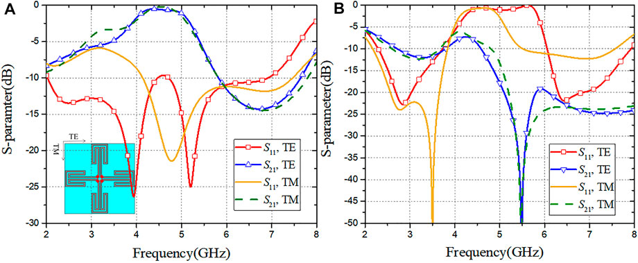
FIGURE 9. (A) S-parameter of reconfigurable FSR with PIN diodes ON. (B) S-parameter of reconfigurable FSR with PIN diodes OFF.
Figure 9 shows the S-parameter of reconfigurable FSR. For TE-polarized incident waves, the FSR can switch between transmission and reflection states. When PIN diodes are turned ON, a wide passband is generated at about 4.5GHz, and there is also an absorptive band ranging from 5.9 to 7 GHz. When PIN diodes are turned off, it will become an A-R-A FSR, the absorption bands are in the range of 2.73–3.76 GHz at a lower frequency, while the upper band ranges from 6.07 to 7.94 GHz. Meanwhile, the reflective band with a value greater than −3 dB spans the frequency ranging from 4.21 to 5.88 GHz. In addition, when the TM-polarized wave is incident, most of its performance is as same as that of the TE wave. The difference is that when the PIN diodes are disconnected, the reflective band is reduced to 4–5 GHz, but the high-frequency absorption band is increased to 5.5–7.5 GHz.
In order to facilitate the measurement and reduce the test space, we use the parallel-plate waveguide (PPW) to measure it. First, the FSR is processed with a length of 14*7 mm and a width of 14 mm. The dielectric substrate is an F4B board with
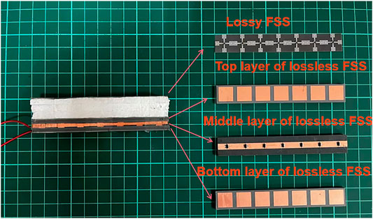
FIGURE10. Structure of fabricated FSR.
To save the cost of a large two-dimensional periodic array, we propose to use a parallel-plate waveguide (PPW). There are two metal plates up and down the PPW, and the surrounding is filled with an absorptive material. Due to the mirror effect of the metal plate, the device of a 1*7 unit in the PPW is equivalent to a two-dimensional periodic array. Figure 11 shows the experiment system configurable for the measurement.
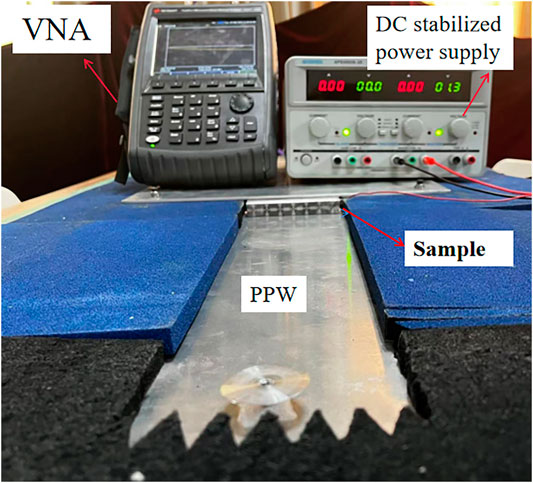
FIGURE 11. Experiment system configurable for the measurement.
The test steps are as follows:
1) First, place the metal block in the middle of the PPW, and take S11 of test results as the background of reflection. In the same way, without anything in the middle of the PPW, the background of S21 is measured.
2) Place the fabricated device in the middle of the parallel-plate waveguide. Note that since the power is fed on the side of the middle layer of the lossless FSS, it is best to put a thin layer of paper on the upper and lower layers when testing to prevent the current from passing through the parallel plate. Then, tests with and without electricity are added. The measured results are obtained by subtracting the background from S11 and S21, respectively.
During the measurement of lossless FSS, we found that there is a frequency offset of the passband. Considering that the parameters of the equivalent circuit of PIN diodes are nonlinear, we measure Lpin of the SMP1345-004LF, which is 0.7nH that differs from 1.5nH in the data sheet. In order to match the measured results, we change l3 to 4 mm for the same frequency of passband as the lossless FSS and bring Lpin = 0.7nH into the simulation.
The measured and simulated results with Lpin = 0.7nH are plotted in Figure 12. The results of measurement and simulation are similar. When PIN diodes are turned ON, a passband around 5 GHz is generated, and the absorption band ranges from 7.2 to 7.5 GHz. When the PIN diodes are in the OFF state, the reflection band less than −3 dB ranges from 4.5 to 5.5 GHz. The high-frequency absorption band and low-frequency absorption band range from 3.3 to 4 GHz and 6.5–7.6 GHz, respectively.
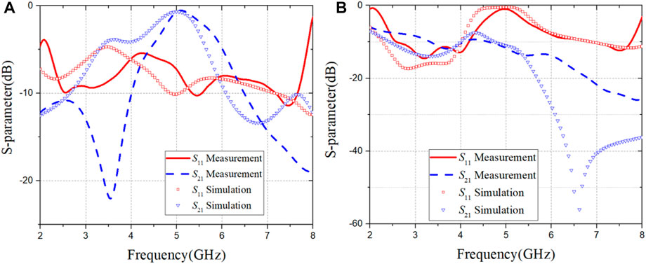
FIGURE 12. (A) Measured and simulated results of reconfigurable FSR with PIN diodes ON. (B) Measured and simulated results of reconfigurable FSR with PIN diodes OFF.
Table 1 demonstrates the comparison between different literature and simulated results of this work. It is clearly observed that this work has the advantage of being a dual-polarization structure and having a wide passband with a relative bandwidth of 32.4%.
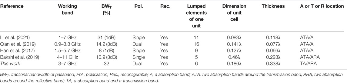
TABLE 1. Comparison of articles.
Though there is a reconfigurable effect, the frequency of the passband shifts to 5 GHz and the absorption band fades away when PIN diodes are in the ON state. The reason for the result is that the Lpin measured is very different from Lpin given by the data sheet. In the simulation, the Lpin has a great impact on the whole simulated results. Figure 13 shows the simulated results of the lossless FSS with changing Lpin when PIN diodes are in the ON state. The change in Lpin not only shifts the frequency but also makes the insertion loss in the passband larger.
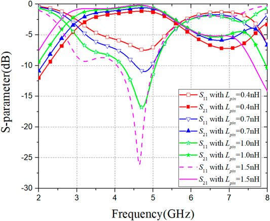
FIGURE 13. Simulated results of lossless FSS with changing Lpin when PIN diodes are turned OFF.
In the general design of FSR, the simulated results are very sensitive to the parameters of PIN diodes, so we need to change the steps of design. Measuring PIN diodes should be considered before you choose a structure of FSR. Then, the measured results of PIN diodes are matched to the simulation of FSR, and the structure is debugged to obtain the desired function.
In this article, a dual-polarization reconfigurable FSR with a wide passband is presented, and the overall structure mainly consists of a top lossy layer and a bottom lossless layer. The design of the lossy layer adopts the method of CMA. Also, the lossless FSS is different from the traditional FSS, which is a coupled FSS to achieve a wide passband. Above and below the middle layer of lossless FSS, there are crossed metal strips with a gap where PIN diodes are mounted to realize dual-polarization and reconfigurable function. The simulated results show a wide passband whose relative bandwidth is 32%. Due to the nonlinearity of PIN diodes, the measured results have a frequency offset. Also, the influence of PIN diodes parameters on the whole simulated results is discussed.
The original contributions presented in the study are included in the article/Supplementary Material; further inquiries can be directed to the corresponding author.
HW wrote the first draft, XK reviewed/edited this manuscript, and XZ help to revise the paper and give the funding support.
Postgraduate Research and Practice Innovation Program of Jiangsu Province (SJCX22_0090).
The authors declare that the research was conducted in the absence of any commercial or financial relationships that could be construed as a potential conflict of interest.
All claims expressed in this article are solely those of the authors and do not necessarily represent those of their affiliated organizations, or those of the publisher, the editors, and the reviewers. Any product that may be evaluated in this article, or claim that may be made by its manufacturer, is not guaranteed or endorsed by the publisher.
Bakshi, S. C., Mitra, D., and Ghosh, S. (2019). A Frequency Selective Surface Based Reconfigurable Rasorber with Switchable Transmission/Reflection Band. Antennas Wirel. Propag. Lett. 18 (1), 29–33. doi:10.1109/lawp.2018.2878858
Chen, Q., Yang, S., Bai, J., and Fu, Y. (2017). Design of Absorptive/Transmissive Frequency-Selective Surface Based on Parallel Resonance. IEEE Trans. Antennas Propagat. 65 (9), 4897–4902. doi:10.1109/tap.2017.2722875
Costa, F., and Monorchio, A. (2012). A Frequency Selective Radome with Wideband Absorbing Properties. IEEE Trans. Antennas Propagat. 60 (6), 2740–2747. doi:10.1109/tap.2012.2194640
Elias, B. B. Q., Soh, P. J., Al-Hadi, A. A., Akkaraekthalin, P., and Vandenbosch, G. A. E. (2021). A Review of Antenna Analysis Using Characteristic Modes. IEEE Access 9, 98833–98862. doi:10.1109/access.2021.3095422
Garbacz, R. J. (1965). Modal Expansions for Resonance Scattering Phenomena. Proc. IEEE 53 (8), 856–864. doi:10.1109/proc.1965.4064
Guo, Q., Su, J., Li, Z., Song, J., and Guan, Y. (2020). Miniaturized-Element Frequency-Selective Rasorber Design Using Characteristic Modes Analysis. IEEE Trans. Antennas Propagat. 68 (9), 6683–6694. doi:10.1109/tap.2020.2986640
Han, Y., Che, W., Xiu, X., Yang, W., and Christopoulos, C. (2017). Switchable Low-Profile Broadband Frequency-Selective Rasorber/Absorber Based on Slot Arrays. IEEE Trans. Antennas Propagat. 65 (12), 6998–7008. doi:10.1109/tap.2017.2759964
Li, R., Hu, H., Tian, J., Li, L., and Bao, Y. (2020). A Switchable A-T-A Rasorber with High Selectivity. In 2020 IEEE International Symposium on Antennas and Propagation and North American Radio Science Meeting: 911-912. doi:10.1109/ieeeconf35879.2020.9329741
Li, R., Tian, J., Jiang, B., Lin, Z., Chen, B., and Hu, H. (2021). A Switchable Frequency Selective Rasorber with Wide Passband. Antennas Wirel. Propag. Lett. 20 (8), 1567–1571. doi:10.1109/lawp.2021.3091480
Qian, G., Zhao, J., Ren, X., Chen, K., Jiang, T., Feng, Y., et al. (2019). Switchable Broadband Dual-Polarized Frequency-Selective Rasorber/Absorber. Antennas Wirel. Propag. Lett. 18 (12), 2508–2512. doi:10.1109/lawp.2019.2941661
Shang, Y., Shen, Z., and Xiao, S. (2014). Frequency-Selective Rasorber Based on Square-Loop and Cross-Dipole Arrays. IEEE Trans. Antennas Propagat. 62 (11), 5581–5589. doi:10.1109/tap.2014.2357427
Shang, Y., Shen, Z., and Xiao, S. (2014). Frequency-selective Rasorber Based on Square-Loop and Cross-Dipole Arrays. IEEE Trans. Antennas Propagat. 62 (11), 5581–5589. doi:10.1109/tap.2014.2357427
Shang, Y., Shen, Z., and Xiao, S. (2013). On the Design of Single-Layer Circuit Analog Absorber Using Double-Square-Loop Array. IEEE Trans. Antennas Propagat. 61 (12), 6022–6029. doi:10.1109/tap.2013.2280836
Shi, Y., Meng, H. X., and Wang, H. J. (2021). Polarization Conversion Metasurface Design Based on Characteristic Mode Rotation and its Application into Wideband and Miniature Antennas with a Low Radar Cross Section. Opt. Express 29 (5), 6794–6796. doi:10.1364/oe.416976
Shi, Y., Meng, Z. K., Wei, W. Y., Zheng, W., and Li, L. (2019). Characteristic Mode Cancellation Method and its Application for Antenna RCS Reduction. Antennas Wirel. Propag. Lett. 18 (9), 1784–1788. doi:10.1109/lawp.2019.2929834
Vogel, M., Gampala, G., Ludick, D., and Reddy, C. J. (2015). Characteristic Mode Analysis: Putting Physics Back into Simulation. IEEE Antennas Propag. Mag. 57 (2), 307–317. doi:10.1109/map.2015.2414670
Wang, L., Liu, S., Kong, X., Zhang, H., Yu, Q., and Wen, Y. (2020). Frequency-Selective Rasorber with a Wide High-Transmission Passband Based on Multiple Coplanar Parallel Resonances. Antennas Wirel. Propag. Lett. 19 (2), 337–340. doi:10.1109/lawp.2019.2962223
Wu, Y., Lin, H., Xiong, J., Hou, J., Zhou, R., Deng, F., et al. (2021). A Broadband Metamaterial Absorber Design Using Characteristic Modes Analysis. J. Appl. Phys. 129 (13). doi:10.1063/5.0043054
Yu, W., Luo, G. Q., Yu, Y., Liao, Z., Jin, H., and Shen, Z. (2019). Broadband Band-Absorptive Frequency-Selective Rasorber with a Hybrid 2-D and 3-D Structure. Antennas Wirel. Propag. Lett. 18 (8), 1701–1705. doi:10.1109/lawp.2019.2928362
Yu, Y., Luo, G. Q., Liu, Q., Yu, W., Jin, H., Liao, Z., et al. (2019). 3D Band-Absorptive Frequency Selective Rasorber: Concept and Analysis. IEEE Access 7, 2520–2528. doi:10.1109/access.2018.2886967
Yuan, H., Li, H., Fang, X., Wang, Y., and Cao, Q. (2021). Active Frequency Selective Surface Absorber with Point-to-Point Biasing Control System. Antennas Wirel. Propag. Lett. 20 (8), 1429–1432. doi:10.1109/lawp.2021.3085424
Zha, D., Cao, Z., Li, R., He, F., Si, K., Dong, J., et al. (2021). A Physical Insight into Reconfigurable Frequency Selective Surface Using Characteristic Mode Analysis. Antennas Wirel. Propag. Lett. 20 (10), 1863–1867. doi:10.1109/lawp.2021.3096324
Keywords: frequency-selective rasorber, frequency-selective surface (FSS), characteristic mode analysis (CMA), parallel-plate waveguide (PPW), characteristic mode theory (CMT)
Citation: Wang H, Kong X and Zhang X (2022) A Dual-Polarized Frequency-Selective Rasorber With a Switchable Wide Passband Based on Characteristic Mode Analysis. Front. Mater. 9:912913. doi: 10.3389/fmats.2022.912913
Received: 05 April 2022; Accepted: 09 May 2022;
Published: 20 June 2022.
Edited by:
Ke Chen, Nanjing University, ChinaReviewed by:
Yajuan Han, Air Force Engineering University, ChinaCopyright © 2022 Wang, Kong and Zhang. This is an open-access article distributed under the terms of the Creative Commons Attribution License (CC BY). The use, distribution or reproduction in other forums is permitted, provided the original author(s) and the copyright owner(s) are credited and that the original publication in this journal is cited, in accordance with accepted academic practice. No use, distribution or reproduction is permitted which does not comply with these terms.
*Correspondence: Xiangkun Kong, eGtrb25nQG51YWEuZWR1LmNu
Disclaimer: All claims expressed in this article are solely those of the authors and do not necessarily represent those of their affiliated organizations, or those of the publisher, the editors and the reviewers. Any product that may be evaluated in this article or claim that may be made by its manufacturer is not guaranteed or endorsed by the publisher.
Research integrity at Frontiers
Learn more about the work of our research integrity team to safeguard the quality of each article we publish.