 Xin Liu
 Yang Liu2,3
 Xue-Hua Liu
 Wen-Li Zhang
 Xu Zuo
94% of researchers rate our articles as excellent or good
Learn more about the work of our research integrity team to safeguard the quality of each article we publish.
Find out more
ORIGINAL RESEARCH article
Front. Mater., 04 May 2022
Sec. Quantum Materials
Volume 9 - 2022 | https://doi.org/10.3389/fmats.2022.872837
This article is part of the Research TopicInnovators in Quantum MaterialsView all 5 articles
The amorphous silicon dioxide-silicon (a-SiO2/Si) interface is an important part of silicon devices. It is difficult to avoid interface defects during the device production process. The passivated interface defects will undergo a depassivation reaction with the protons in the silicon dioxide generated by irradiation and convert to positively charged dangling bonds, thereby affecting device performance. In engineering practice, there is a final passivation layer on top of a-SiO2, and it is inevitable to introduce stress on the a-SiO2/Si interface. Therefore, studying the depassivation reaction mechanism of a-SiO2/Si interface defects under stress is of great significance to understand the performance degeneration in real devices. By using molecular dynamics and first-principles calculations, Pb defects at a-SiO2/Si (111) interface and Pb1 defects at a-SiO2/Si (100) interface are selected in this work to investigate the effect of stress on their depassivations. Biaxial strains are applied to the models, energy curves of the depassivation reactions under stress are calculated using the CI-NEB (Climbing Image Nudged Elastic Band) method, and transition states are identified. According to the Harmonic Transition State Theory (HTST), the reaction rate constants of the depassivation reactions of Pb and Pb1 defects at a certain temperature can be obtained. Finally, the relative concentration curves during depassivation reactions of PbH and Pb1H under stress and room temperature are obtained. Detailed data and figure analyses are presented to demonstrate differences between the two typical interface defects when depassivating under stress. Appropriate degrees of interface stress are proved to extend the depassivation time of defects, therefore prolonging the service life of devices.
As the key to integrated circuit technology, MOS structure is the core part of most silicon devices (Hughes and Benedetto, 2003). As an important part of MOS devices, the a-SiO2/Si interface has a significant impact on the reliability of the device (Hughes and Benedetto, 2003). How to extend the service life of the device is an urgent problem to be solved. The main cause of device performance degradation is the existence of interface dangling bond defects. In the process of device fabrication, those defects are usually passivated by hydrogen and lose their electrical activity. However, when the device is exposed to ionization radiation, the protons generated by the radiation will react with the passivated defects and convert them into positively charged dangling bonds, resulting in the degeneration of device performance (Rashkeev et al., 2001; Godet and Pasquarello, 2006; Li et al., 2018). Meanwhile, the radiation dose rate also impacts the degree of device ionization damage. Experiments showed that the ionization damage in a low-dose rate irradiation environment is more serious than that in a high-dose rate, which is called Enhanced Low-Dose-Rate Sensitivity (ELDRS) (Witczak et al., 2005; Pease et al., 2008; Chen, 2010). It was pointed out that the ELDRS effect is likely to be associated with the interface stress, and it is possible to relieve the ELDRS effect by removing the final passivation layer of the device (Shaneyfelt et al., 2002). Although the microscopic mechanisms behind the ELDRS effect is unknown at present, stress, as one of the known factors that affect ELDRS, should be paid special attention to in the selection of the final passivation layer materials and the encapsulation process of the device (Shaneyfelt et al., 2002; Boch et al., 2003; Shaneyfelt et al., 2003). Therefore, studying the influence of stress on the depassivation reactions of a-SiO2/Si interface defects is highly valuable in reducing or even eliminating the ELDRS effect, improving the stability of the device, and extending the service life of the device in extreme environment.
Dangling bond defects at SiO2/Si interfaces are usually called Pb-type defects. Experiments showed that all Pb-type defects share the same configuration [·Si(-Si)3] and the same chemical properties. For example, Pb defects are all amphoteric (Lenahan, 2003). When the Fermi level is below the +/0 charge state transition level, the defect will trap holes and is positively charged. The angle between the three backward Si-Si bonds becomes larger and the defect becomes an approximate planar structure, and this structure implies sp2 hybridization in electronic structure. When the Fermi level is between the transition level +/0 and 0/-, the defect is electrically neutral. When the Fermi level is above the 0/- transition level, the defect will trap electrons and becomes negatively charged. The angle between the three backward Si-Si bonds becomes smaller, and the defect shows a stretched tetrahedral structure (Kovačević and Pivac, 2014). There are differences in their physical properties. Pb defects are located at the a-SiO2/Si (111) interface, while Pb0 and Pb1 defects are located at the a-SiO2/Si (100) interface. The dangling bonds of Pb and Pb0 defects are along the [111] direction of crystalline silicon, while the Pb1 dangling bond is roughly along the [211] direction (Stesmans et al., 1998). For the Pb1 defect, there are three candidating configurations: dimer, bridge and AOD, among which the AOD configuration is more reasonable than the dimer and bridge configurations (Poindexter et al., 1981; Stesmans et al., 1998; Stirling et al., 2000; Stirling and Pasquarello, 2005).
The depassivation reaction process of Pb-type defects on the SiO2/Si interface has been intensively investigated. Brower et al. showed that the depassivation reaction takes place in two steps. After a proton arrives at the interface, it first captures an electron and becomes an electrically neutral hydrogen atom, and then the hydrogen atom reacts with the passivated dangling bond:
In this work, by the first-principles calculation method based on Density Functional Theory (DFT), the reaction is simulated under different interface stresses. We choose the two most common Pb-type defects: Pb and Pb1 (AOD), focus on the reaction processes of Pb and Pb1 defects (PbH and Pb1H) being depassivated by protons to Pb+ and Pb1+ under stresses, and summarize the influence of stress on the depassivation reaction of Pb and Pb1 defects. Following the viewpoint of Rashkeev et al., we simulate reactions that H+ depassivates PbH or Pb1H to generate a positively charged dangling bond:
The a-SiO2/Si (100) and (111) interface models used in this work are derived from our previous works (Li et al., 2019a; Li et al., 2019b; Hong and Zuo, 2020). From a-SiO2 and crystalline Si, the models are constructed through thermally oxidization of Si by a-SiO2 using the Large-scale Atomic/Molecular Massively Parallel Simulator (LAMMPS) code (Plimpton, 1995; van Duin et al., 2001; van Duin et al., 2003; Fogarty et al., 2010). Passivation can improve the stability of the structure and properties, so it has important scientific significance and broad application prospects (Ya-Hui et al., 2020). In this manuscript, hydrogen is used to passivate dangling bond defects produced during interface thermal oxidation. Dimensions of the final a-SiO2/Si (100) and (111) interface models are 15.5 Å × 15.5 Å × 35.0 Å and 13.3 Å × 15.4 Å × 49.4 Å, respectively. In the a-SiO2/Si (100) interface model, the thicknesses of the seven-layer Si (100) moiety and a-SiO2 moiety are 8.1 Å and 12.7 Å, respectively, with a vacuum layer of 11.8 Å and a hydrogen passivation layer of 2.4 Å. In the a-SiO2/Si (111) interface model, the thicknesses of the eight-layer Si (111) moiety and a-SiO2 moiety are 10.2 Å and 15.1 Å, respectively, with a vacuum layer of 20.9 Å and a hydrogen passivation layer of 3.2 Å.
The first-principle calculations based on the Density Functional Theory are performed with the plane-wave basis, as implemented in the Vienna ab initio simulation package (VASP) (Kresse and Furthmüller, 1996). The electron core interaction is included by using the frozen-core all-electron projector augmented wave (PAW) method (Blöuml, 1994). The exchange correlation functional is treated by the generalized gradient approximation (GGA) parameterized by PERDEW, BURKE and ERNZERHOF (PBE) (Perdew et al., 1996). The plane-wave basis set cut-off energy is set as 520 eV for all calculations. Since the a-SiO2/Si models are large in size, the Brillouin-zone integration is limited to the Γ point only. The structure is relaxed until the total energy is minimized. The convergence criterion of structural optimization is that the total energy difference is less than 10−5 eV, and the force on each atom is smaller than a tolerance of 0.05 eV/Å.
Harmonic Transition State Theory (HTST) (Vineyard, 1957) is derived from a well-known theory—Transition State Theory (TST) (Henry, 1935; Voter and Doll, 1984). For many solid-state reactions, HTST is a good approximation as the energy barrier is usually larger than the average kinetic energy kBT in system. Another reason for using HTST as a reasonable approximation is that the harmonic approximation is often effective. Near the saddle point, the potential energy increases rapidly and forms a small bottleneck area. When using HTST, the first step is to find the saddle point corresponding to the reaction. There are many ways to find saddle points, and in this study we will use Climbing Image–Nudged Elastic Band (CI-NEB) method.
G. Henkelman developed the CI-NEB method to search for a transition state which is the first-order saddle point (Henkelman et al., 2000). The CI-NEB method specifically considers the problem of locating the transition state. The key difference between CI-NEB and Nudged Elastic Band (NEB) is the definition of the force on the point with the highest energy. In CI-NEB, this point will not be subjected to the spring force of the adjacent points, which can prevent its position from being pulled away from the transition state, therefore making this point climb to the transition state along the path in the direction of energy increase. The CI-NEB method requires only a few points, such as a total of five or even three points including the initial and final states to accurately locate the transition state. It is one of the most efficient methods to find a transition state. Between the initial and final structures of a reaction, appropriate number of images are inserted. In this work, the transition state and activation energy of the Pb-type defect depassivation reaction are obtained by the CI-NEB method.
In order to simulate the stress induced by the final passivation layer, a biaxial strain is applied at the a-SiO2/Si (111) and (100) interfaces (Zhou et al., 2014; Grote and Berger, 2015; Al-Shami et al., 2018). The biaxial strain is imposed on the relaxed unit cell along x-axis and y-axis ([100] and [010] direction) according to the equations (Al-Shami et al., 2018):
Taking the Pb defect at a-SiO2/Si (111) interface as an example, the concentration ratio of depassivated defects and passivated defects in an initial condition is deduced. Derived formulas are also applicable to the Pb1 defect at a-SiO2/Si (100) interface.
From the above introduction, the reaction of PbH depassivated by H+ is:
where kd is the depassivation reaction rate constant. According to the chemical reaction kinetic theory (HSteinfeld et al., 1999), the reaction rate equation can be written as:
where [Pb+] is the concentration of Pb+, [PbH] is the concentration of PbH, and [H+] is the concentration of H+, which depends on its diffusion. Eq. 2 can also be written as:
where N0 is the total density of the PbH center in the initial condition. Set
The solution of the above first-order differential equation is:
where t is time. The above approximation holds for the slow depassivation at a low proton concentration.
Therefore, the key to solving the relative concentration x of interface defects Pb+ and Pb1+ during the depassivation reaction is to solve the reaction rate constant kd. From the Arrhenius equation, we can write the depassivation reaction rate constants kd and kds (Brower and Myers, 1990) as follows,
where Ed is the activation energy of the depassivation reaction without stress, and Eds is the activation energy of the depassivation reaction under stress. kds0 and kd0 are the pre-exponential factors for the depassivation reaction with and without stress, respectively. kB is Boltzmann’s constant equal to 1.38 × 10⁻²³ J/K, T is temperature (unit: K), and the relevant reduction unit of Boltzmann’s constant kBT is 25.852 meV (T = 300 K).
According to the Harmonic Transition State Theory (HTST), the activation energy and transition state can be calculated by the CI-NEB method, and then the reaction rate can be calculated by the following equation:
where N is the number of atoms,
Structures of the Pb defect are shown in Figures 1C,D. Si(1) is the defective atom, and the three silicon atoms bonded with Si(1) are directly connected to the crystalline silicon moiety through Si-Si bonds. In order to simulate the depassivation reaction of the Pb defect at the a-SiO2/Si (111) interface, the initial and final states of the reaction need to be constructed first. In the initial state of the reaction, the defective atom Si(1) is passivated with the atom H(1), and the proton H(2) is stably connected to the Si-O(1)-Si bridge (Yue et al., 2018). In the final state of the reaction, a hydrogen molecule is formed in the void near the defect. It is worth mentioning that before carrying out further calculations, the stability of the initial and final state structures needs to be confirmed (Pei et al., 2021; Ying-Ying et al., 2021). The atomic vibrational frequencies of initial and final state structures must be calculated first to make sure that there is no imaginary frequency. It is based on this operation that the reaction processes can be simulated correctly in this manuscript. The initial and final states of the Pb defect depassivation reaction are shown in Figure 1.
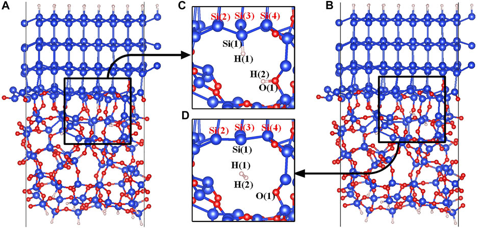
FIGURE 1. (A) The initial state model of the a-SiO2/Si (111) interface, (B) The final state model of the a-SiO2/Si (111) interface, (C) The initial state (state 00) partial figure of the Pb defect depassivation, and (D) The final state (state 04) partial figure of the Pb defect depassivation. Blue, red and white balls represent Si, O and H atoms, respectively.
Since the Pb defect generated by the depassivation is positively charged, the defective Si atom and the surrounding three silicon atoms form a nearly planar structure in the final state, as shown in Figure 1D. The tetrahedral distortion parameter t is defined as
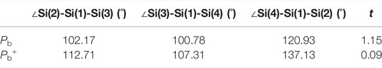
TABLE 1. Three Si-Si-Si bond angles and the parameter t.
In the initial state 00 of the depassivation reaction, the bond lengths of Si(1)-H(1) and O(1)-H(2) are 1.508 and 0.984 Å, respectively, and the distance between H(1) and H(2) is 2.857 Å. From the initial state 00 to the state 02, H(1) and H(2) tend to move towards each other, and the lengths of Si(1)-H(1) and O(1)-H(2) bonds keep increasing until the bonds are broken. When the reaction proceeds to the transition state 02, the energy of the system reaches a highest point of 1.398 eV. In the 02 state, the distances between Si(1) and H(1), O(1) and H(2), and H(1) and H(2) are 1.889, 1.323, and 1.100 Å, respectively. As the reaction proceeds from state 02 to state 04, the distance between H(1) and H(2) is decreasing, while the distances between Si(1) and H(1), and O(1) and H(2) keep increasing. In the final state 04, the H(1)-H(2) bond length stabilizes at a value of 0.755 Å. The three intermediate states and the energy profile curve are shown in Figure 2. The bond lengths and energies of the states during the depassivation reaction are listed in Table 2.
FIGURE 2. Intermediate states and energy profile curve of the Pb defect depassivation reaction. (A) 01 state, (B) 02 state, (C) 03 state, and (D) energy profile curve.
TABLE 2. H-H, Si-H and O-H bond lengths, and the energies of the states in Pb depassivation reaction.
It can be extracted from Figure 2D that the 02 state is the transition state and the activation energy is 1.398 eV. VASP is hired to calculate the vibration frequencies. There is no imaginary frequency in the initial and final states, and there is one and only one in the transition state. The calculated pre-exponential factor is 1.44 × 10⁻⁷ cm3s−1.
Structures of the Pb1(AOD) defect are shown in Figures 3C,D. Si(1) is the defective atom, and Si(4) as one of the three silicon atoms connected to Si(1), is linked to the a-SiO2 moiety through one Si-O-Si bridge and to the crystalline silicon moiety through two Si-O-Si bridges. In the initial state of the Pb1(AOD) defect depassivation, the proton H(1) is stably connected to the Si-O(1)-Si bridge to form the O(1)-H(1) bond (Yue et al., 2018), and the atom H(2) is chosen to passivate the defective atom Si(1). In the final state, a hydrogen molecule is formed in the void near the Pb1+ defect. The initial and final state diagrams are shown in Figure 3.
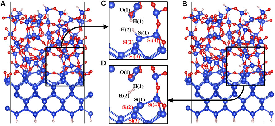
FIGURE 3. (A) The initial state model of the a-SiO2/Si (100) interface, (B) The final state model of the a-SiO2/Si (100) interface, (C) The initial state (state 00) partial figure of the Pb1 defect depassivation, and (D) The final state (state 04) partial figure of the Pb1 defect depassivation. Blue, red and white balls represent Si, O and H atoms, respectively.
It can be seen from the final state partial Figure 3D that the defective silicon atom Si(1) and the surrounding three atoms form a plane-like structure. The comparisons between the Pb1 defect and the Pb1+ defect on three Si-Si-Si bond angles and the parameter t are listed in Table 3. When the Pb1 defect is neutral, the t parameter is 1.25 close to the value of one for a perfectly sp3 hybridized atom. For the positively charged Pb1+ defect, the t value is 0.41 close to the perfect sp2 hybridization value zero.

TABLE 3. Three Si-Si-Si bond angles and the parameter t.
In the initial state 00, the bond lengths of Si(1)-H(2) and O(1)-H(1) are 1.501 Å and 0.989 Å, respectively, and the distance between H(1) and H(2) is 2.665 Å. From the initial state 00 to the intermediate state 01, H(1) gradually separates from O(1), and H(2) gradually separates from Si(1). When the reaction proceeds to the 02 state, the system energy reaches the maximum value of 0.931 eV. In the 02 state, the distances between Si(1) and H(2), O(1) and H(1), and H(1) and H(2) are 1.758, 1.353, and 1.035 Å, respectively. As the reaction progresses, the distance between Si(1) and H(2) keeps increasing, and the distance between O(1) and H(1) is also gradually increasing while the distance between H(1) and H(2) is gradually decreasing. Finally the reaction proceeds to the final state 05, where the H(1)-H(2) bond length is 0.740 Å. The four intermediate states diagrams and the energy profile curve are shown in Figure 4. The bond lengths and energies of the states during the depassivation reaction are listed in Table 4.
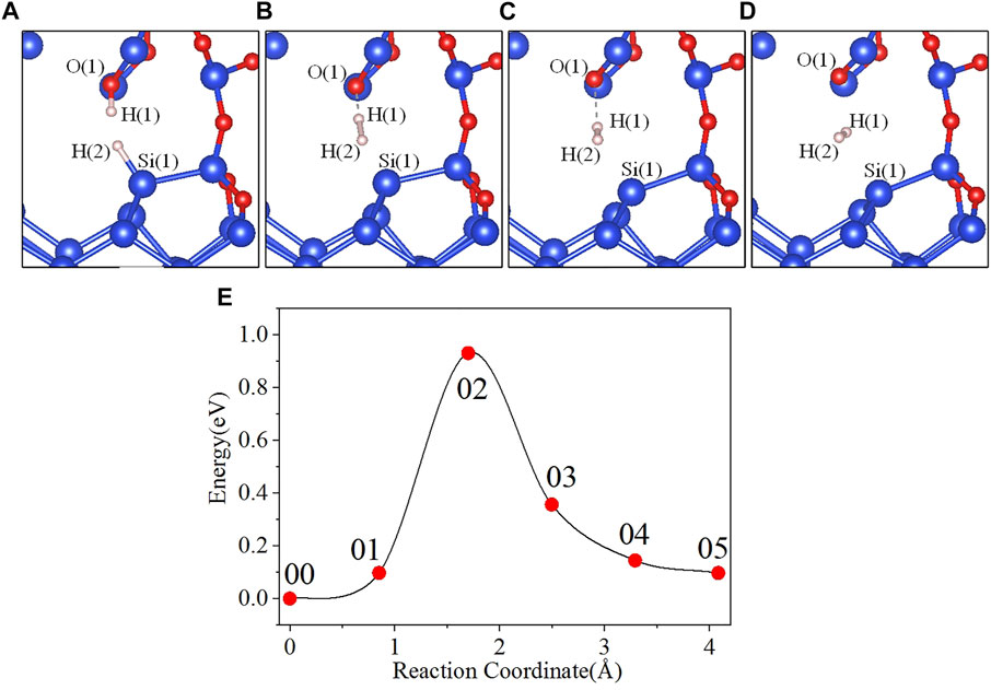
FIGURE 4. Intermediate states and energy profile curve of the Pb1 defect depassivation reaction. (A) 01 state, (B) 02 state, (C) 03 state, (D) 04 state and (E) energy profile curve.
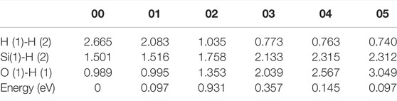
TABLE 4. H-H, Si-H and O-H bond lengths and the energies of the states in Pb1 depassivation reaction.
In Figure 4E, the 02 state is the transition state, and the activation energy is 0.931 eV. VASP is used to calculate the vibration frequencies and there is no imaginary frequency in the initial and final states, and one and only one in the transition state. The calculated pre-exponential factor is 2.71 × 10⁻⁸ cm3s−1.
In order to simulate the stress induced by the final passivation layer, a biaxial strain is applied to the a-SiO2/Si (111) and (100) interfaces, and the strain degree ε ranges from −7% to 7% with a step of 1%. The stress-strain scatter diagrams are shown in Figure 5. The external pressure is the equivalent pressure on the interface after stress is applied. A positive value indicates that the interface is compressed, and a negative value indicates that the interface is stretched. It is shown by the figure that the external pressure (or its absolute value) is almost linearly proportional to the strain degree.
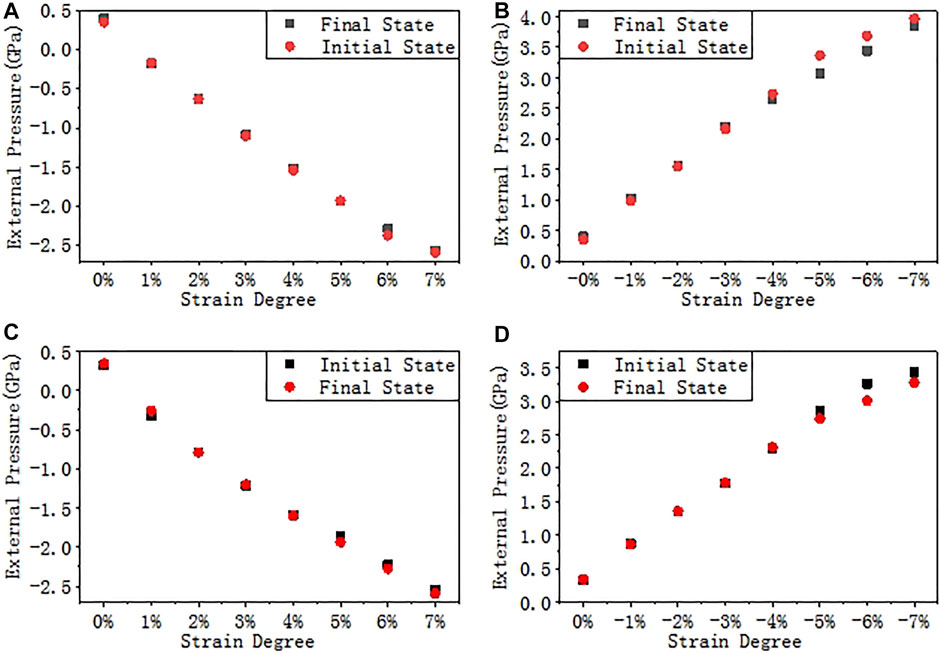
FIGURE 5. Stress-strain curves. (A) Tensile strain on interface (111), (B) Compressive strain on interface (111), (C) Tensile strain on interface (100), and (D) Compressive strain on interface (100).
In addition to the stress-strain curves, the change of average bond length and average bond angle also reflects the degree of deformation of models to a certain extent. In order to facilitate a more detailed analysis of the structural properties of models, and to further verify the rationality of the stress applied, a statistical analysis of the bond lengths and bond angles is conducted, including the average values and the increase rates. The increase rate is defined as the ratio of the increase value of bond length (or bond angle) in a certain stage to the initial value. Tables 5, 6, respectively show the average lengths of Si-O bond in a-SiO2 part and Si-Si bond in crystalline silicon part, and the average angles of ∠O-Si-O and ∠Si-O-Si in a-SiO2 part with strains of −7%, 0% and 7%.
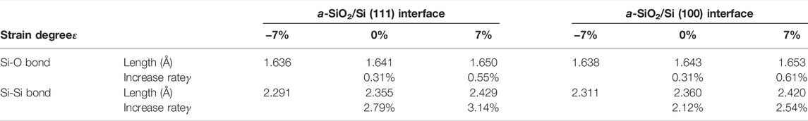
TABLE 5. The average lengths and increase rates of Si-O bond and Si-Si bond at different strains.
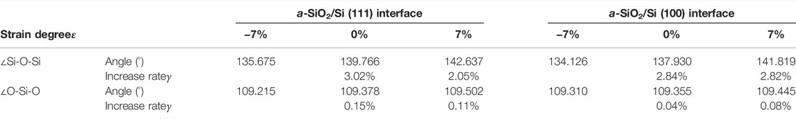
TABLE 6. The average angles and increase rates of ∠O-Si-O and ∠Si-O-Si at different strains.
It is shown by the above two tables that, as the strain degree ε of the a-SiO2/Si interface increases from −7% to 7%, the average values of bond lengths and bond angles also increase. However, the increase rate γ is different. When ε increases in a certain extent, i.e., from −7% to 0% or from 0% to 7%, the Si-Si bond exhibits a higher average increase rate of 2.65%, while that of the Si-O bond is 0.45%. It can be concluded that the Si-Si bond is relatively more sensitive to stress. For the bond angles, ∠Si-O-Si has an average increase rate of 2.68% while ∠O-Si-O has an average increase rate of 0.10%. It can be seen that compared to ∠O-Si-O, ∠Si-O-Si is more sensitive to stress.
After applying stress to the interface models, the depassivation reactions of the interface defects under different stresses are investigated. Tensile and compressive strains are applied to the a-SiO2/Si (111) and (100) interfaces and the activation energies of Pb and Pb1 defects depassivations under different strains are listed in Tables 7, 8. The energy curves during depassivation reactions and activation energy profile curves (Figures 6–9) under different stresses are shown below.
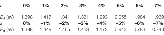
TABLE 7. Activation energies of Pb defect depassivations under tensile and compressive strains.
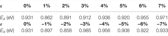
TABLE 8. Activation energies of Pb1 defect depassivations under tensile and compressive strains.
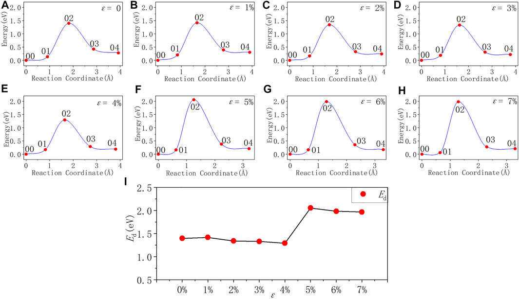
FIGURE 6. Reaction energy curves and activation energy profile curve of the Pb defect depassivation; (A–H) exhibit depassivation reaction energy curves under a tensile strain range of 0%∼7%, and (I) exhibits the activation energy profile curve.
From Figure 6 and Table 7, it can be concluded that when the tensile strain degree ε is between 0% and 4%, the activation energy of Pb defect depassivation reaction is stable at about 1.35 eV, and the fluctuation range is less than 0.07 eV. When the strain degree ε increases from 4% to 5%, the activation energy surges by 0.76–2.05 eV. Afterwards as the strain degree ε increases, the activation energy stabilizes at a higher value of about 2.00 eV.
In Figure 7 and Table 7, as the strain degree ε decreases from 0% to −3%, the Pb depassivation reaction activation energy stabilizes at about 1.40 eV, and the fluctuation is less than 0.07 eV. Within this strain range, the forward reaction barrier of the depassivation reaction is always higher than the reverse one. When the strain degree ε decreases from −3% to −4%, the activation energy drops drastically to 1.17 eV, and the forward reaction barrier becomes smaller than the reverse reaction barrier. Then, as the strain degree ε decreases from −4% to −7%, the reaction activation energy also gradually decreases and is less than 1 eV, and the forward reaction barrier of the reaction is always smaller than the reverse one.
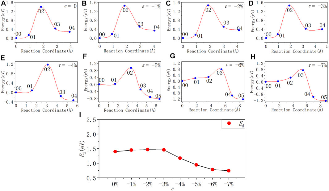
FIGURE 7. Reaction energy curves and activation energy profile curve of the Pb defect depassivation; (A–H) exhibit depassivation reaction energy curves under a compressive strain range of 0%∼−7%, and (I) exhibits the activation energy profile curve.
In Figure 8 and Table 8, as the tensile strain degree ε increases, the activation energy of the Pb1 defect depassivation reaction does not change much. It is basically stable at about 0.90 eV and the fluctuation is less than 0.08 eV. From the depassivation reaction curves, when ε increases to 6%, the reverse reaction barrier of the depassivation reaction becomes higher than the forward reaction barrier.
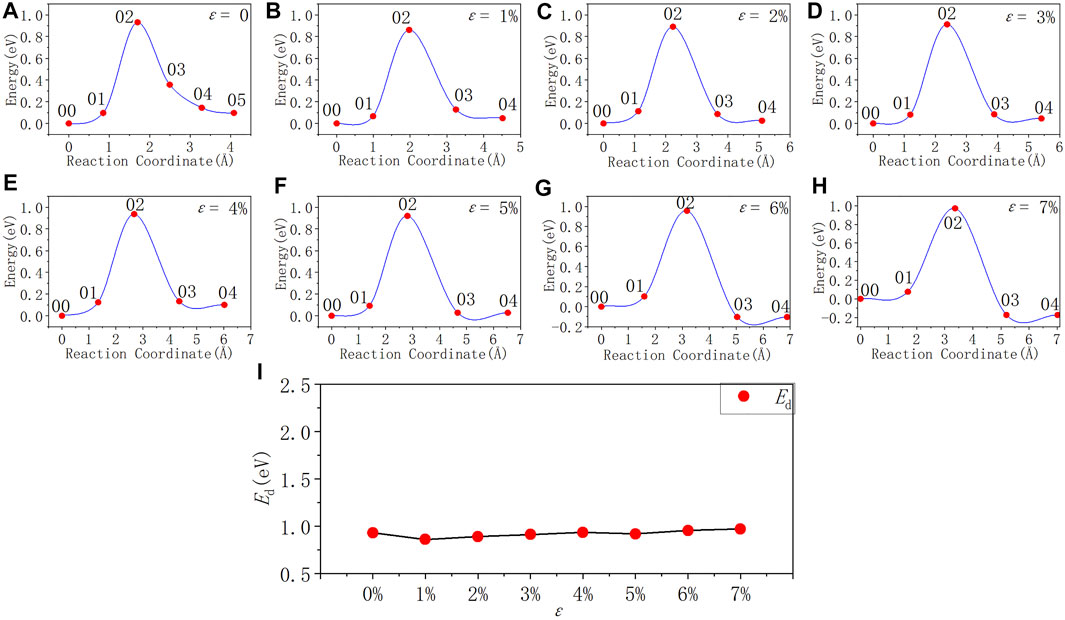
FIGURE 8. Reaction energy curves and activation energy profile curve of the Pb1 defect depassivation; (A–H) exhibit depassivation reaction energy curves under a tensile strain range of 0%∼7%, and (I) exhibits the activation energy profile curve.
In Figure 9 and Table 8, the activation energy of the depassivation reaction of Pb1 defects is stable at about 0.92 eV under compressive strain, and the fluctuation is less than 0.07 eV. As the degree of compressive strain increases, the reverse reaction barrier becomes higher than the forward one.
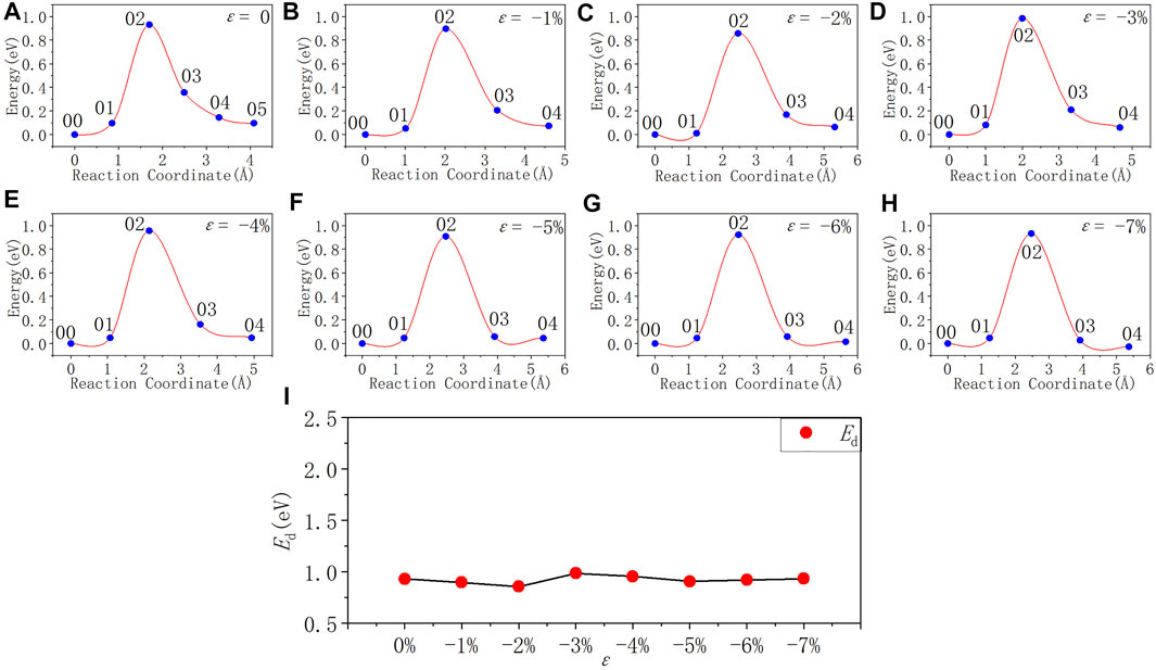
FIGURE 9. Reaction energy curves and activation energy profile curve of the Pb1 defect depassivation; (A–H) exhibit depassivation reaction energy curves under a compressive strain range of 0%∼−7%, and (I) exhibits the activation energy profile curve.
According to Eq. 8, as long as the activation energy and the pre-exponential factor are obtained, the reaction rate kd can be solved for a chemical reaction. The pre-exponential factor is the ratio of the product of the vibration frequencies of the initial state and the product of all real vibration frequencies of the transition state of the reaction. In this study, VASP code is used to calculate pre-exponential factors of different depassivation reactions. Combined with the reaction activation energy shown in the previous part, the depassivation reaction rates of Pb and Pb1 defects under different strain degrees at room temperature (300K) are calculated. The results are exhibited in Tables 9, 10 and curves are plotted in Figure 10.
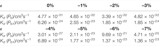
TABLE 9. Depassivation reaction rates of Pb and Pb1 defects under compressive strains at 300 K.
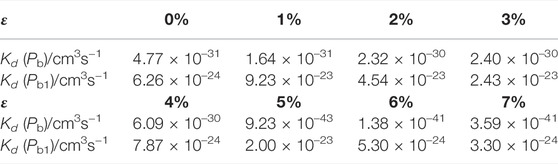
TABLE 10. Depassivation reaction rates of Pb and Pb1 defects under tensile strains at 300 K.
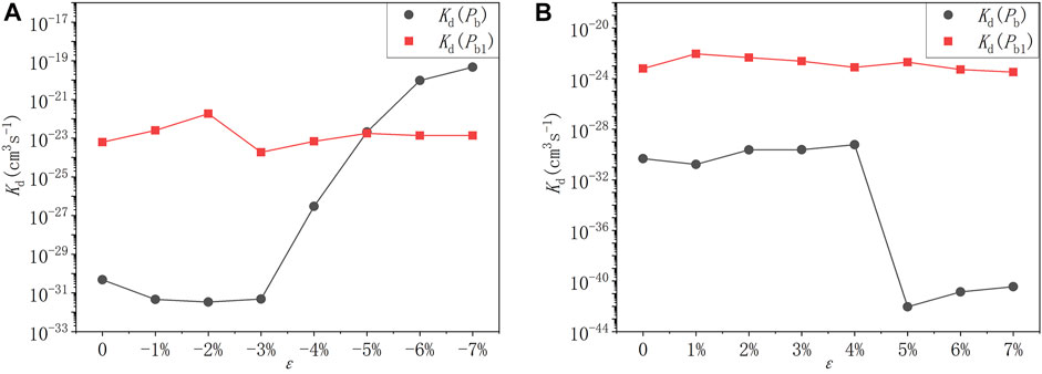
FIGURE 10. The depassivation reaction rate curves of Pb and Pb1 defects under (A) compressive strains and (B) tensile strains at room temperature (300K).
It can be seen that at room temperature the depassivation reaction rate of Pb1 defects is generally faster than that of Pb defects. For Pb defects, when the strain degree ε is 5%, the depassivation reaction rate is the slowest; when ε is −7%, the depassivation reaction rate is the fastest. In addition, when the strain degree ε is in the range of −7%∼−5%, the depassivation reaction rate is relatively fast, which is 8–11 orders of magnitude faster than that without stress; when ε is in the range of 5%–7%, the depassivation reaction rate is relatively slow, which is 10–12 orders of magnitude slower than that in the case of no stress. For Pb1 defects, the depassivation reaction rate changes generally steady, and there is no significant increase or decrease as stress is applied. When the strain degree ε = -2%, the depassivation reaction rate is the fastest, which is two orders of magnitude faster than that without stress. The increase or decrease of depassivation rate under other strain degrees is insignificant. It can be inferred that the depassivation of Pb1 defects on the a-SiO2/Si (100) interface is insusceptible of stress, while the depassivation of Pb defects on the a-SiO2/Si (111) interface can be greatly affected by stress.
After obtaining the depassivation reaction rate constant kd, the curve of the relative concentration value (x) of the defect with time (t) can be calculated according to Eq. 5. Researchers have studied the hydrogen/deuterium diffusion in solid-state crystallized (SSC) poly-Si and low-pressure chemical-vapor-deposited (LPCVD)-grown polycrystalline silicon. The study pointed out that the H surface concentration amounts to ≈1019 and ≈3×1019 cm−3 in LPCVD-grown and SSC poly-Si, respectively (Nickel et al., 1996). Based on the previous research [H+] in Eq. 5 is set to 1019 cm−3 in our work, and the relative concentration xPb and xPb1 of Pb and Pb1 defects as a function of time are plotted in Figure 11.
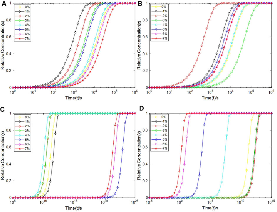
FIGURE 11. The relative concentrations of Pb+ and Pb1+ as a function of time during depassivation processes. (A) The relative concentration of Pb1+ under tensile strains, (B) The relative concentration of Pb1+ under compressive strains, (C) The relative concentration of Pb+ under tensile strains, and (D) The relative concentration of Pb+ under compressive strains.
It can be seen from Figure 11 that compared with the Pb defect, the depassivation of the Pb1 defect is relatively insensitive to stress, which can be explained through their local structures. For the Pb1 defect, one of the three silicon atoms bonded to the defective atom is also bonded to three oxygen atoms, so the defective silicon atom is connected to the silicon substrate through a [·Si-Si-(O)2-Si] structure, whereas the defective silicon atom of the Pb defect is directly connected to the silicon substrate through a [·Si-Si] structure. In a nutshell, the Si-O-Si bridge exists in the Pb1 defect, but not in the Pb defect. The different depassivation performances for the two defects under stress are owing to the softness of the Si-O-Si bridge. Compared to the Si-Si-Si bond angle, the energy required to change the Si-O-Si bond angle is much lower, so the Pb1 defect can release local stress through a torsion of its structure, therefore making itself insensitive to stress (Li et al., 2019b). However, the Pb defect is short of a structure like the Si-O-Si bridge, so it is more sensitive to the applied stress.
For Pb1H defects at a-SiO2/Si(100) interface, it takes up to 103–106 s to depassivate them with protons to Pb1+ at room temperature, which is consistent with the experimental results summarized by Schwank et al. (2008) on the accumulation rate of interface traps. When the strain degree ε of the a-SiO2/Si(100) interface is −2%, 1% or 2% (equivalent to the interface pressure of about 1.36 GPa, −0.30 GPa or −0.80 GPa), the depassivation reaction rate of Pb1H defects is the fastest. The total time for protons to depassivate all Pb1H into Pb1+ is about 103–104s. When ε is −3%, 6% or 7% (equivalent to the interface pressure of about 1.78 GPa, −2.30 GPa or −2.60 GPa), the depassivation reaction rate of Pb1H defects is the slowest. At this time, it takes about 105–106 s for the Pb1H depassivation reaction to reach saturation.
For PbH defects at a-SiO2/Si (111) interface, stress greatly impacts the time taken for the depassivation reaction. When the strain degree ε of a-SiO2/Si (111) interface is −5%, −6% or −7% (equivalent to the interface pressure of about 3.20, 3.50 or 3.90 GPa), the PbH depassivation reaction rate is relatively high, and all PbH depassivation reactions can reach saturation within 105 s, especially when ε is −6% or −7%, it takes only 102 s to depassivate all PbH into Pb+ defects. When the strain degree ε of a-SiO2/Si (111) interface is 5%, 6%, 7% (equivalent to the interface pressure of about −1.90, −2.30 GPa or −2.60 GPa), the PbH depassivation reaction rate is very slow. In these cases, the time needed to depassivate all PbH at the interface to Pb+ is about 1023∼1024 s.
The first-principles calculation method based on density functional theory is hired to investigate the impact of stress on the depassivation reaction of Pb defects at a-SiO2/Si (111) interface and Pb1 defects at a-SiO2/Si (100) interface. In order to simulate the final passivation layer stress of the interfaces, biaxial strain is applied to the model, and stress-strain curves are plotted to verify the rationality of the stress application. Based on the kinetic theory of Pb-type defect proton depassivation, the equation of the relative concentration x of interface defects is derived. The HTST theory combined with the CI-NEB method is hired to calculate the depassivation reaction rate constant kd. Finally, the relative concentration change curves of Pb defects and Pb1 defects during depassivation under different stresses are illustrated.
It is shown that stress has an obvious impact on the depassivations of the Pb defect and the Pb1 defect, as reflected in the reaction activation energy and reaction rate. By applying different degrees of stresses, the depassivation reaction rates of the Pb defect can be 10 orders of magnitude slower or faster than that under no stress, and the reaction time can be controlled from 101 to 1025 s. In contrast, the depassivation reaction of the Pb1 defect is insensitive to the applied stress because of its local structure. Under different stresses, the depassivation reaction rates hardly show an excessive increase or decrease, and the depassivation reaction time is stably distributed in the range of 103–106 s, which is consistent with the experimental data given in the literature. It has been shown that stress can impact radiation-induced charge buildup in MOS structures, and it is also responsible for the ELDRS (Chin and Ma, 1983; Zekeriya and Ma, 1984; Kasama et al., 1986; Shaneyfelt et al., 2002; Boch et al., 2003; Shaneyfelt et al., 2003). We show that the Pb defect is more sensitive to the applied stress, hinting that stress may be an effective way to control its properties. It could be predicted that the stress may impact the Pb defect and then influence ELDRS indirectly.
The raw data supporting the conclusion of this article will be made available by the authors, without undue reservation.
XZ and XL conceived the idea. XH-L performed the DFT calculations and data analysis. XL wrote the manuscript and XZ provided writing guidance. All authors discussed the results. XZ and YL supervised the execution of the whole work. All authors listed have made a substantial, direct and intellectual contribution to the work, and approved it for publication.
This research is supported by the Science Challenge Project (Grant No. TZ2016003-1-105), the Tianjin Natural Science Foundation (Grant No. 20JCZDJC00750), and the Fundamental Research Funds for the Central Universities–Nankai University (Grant No. 63211107 and 63201182).
The authors declare that the research was conducted in the absence of any commercial or financial relationships that could be construed as a potential conflict of interest.
All claims expressed in this article are solely those of the authors and do not necessarily represent those of their affiliated organizations or those of the publisher, the editors, and the reviewers. Any product that may be evaluated in this article, or claim that may be made by its manufacturer, is not guaranteed or endorsed by the publisher.
Al-Shami, A., Lakhal, M., Hamedoun, M., El Kenz, A., Benyoussef, A., Loulidi, M., et al. (2018). Tuning the Optical and Electrical Properties of Orthorhombic Hybrid Perovskite CH3NH3PbI3 by First-Principles Simulations: Strain-Engineering. Solar Energ. Mater. Solar Cell. 180, 266–270. doi:10.1016/j.solmat.2017.06.047
Blöchl, P. E. (2000). First-principles Calculations of Defects in Oxygen-Deficient Silica Exposed to Hydrogen. Phys. Rev. B 62 (10), 6158–6179. doi:10.1103/physrevb.62.6158
Blöuml, P. E. (1994). Projector Augmented-Wave Method. Phys. Rev. B. 50 (24), 17953–17979. doi:10.1103/physrevb.50.17953
Boch, J., Fleetwood, D. M., Schrimpf, R. D., Cizmarik, R. R., and Saigne, F. (2003). Impact of Mechanical Stress on Total-Dose Effects in Bipolar ICs. IEEE Trans. Nucl. Sci. 50, 2335–2340. doi:10.1109/tns.2003.820768
Brower, K. L., and Myers, S. M. (1990). Chemical Kinetics of Hydrogen and (111) Si‐SiO2interface Defects. Appl. Phys. Lett. 57 (2), 162–164. doi:10.1063/1.103971
Chen, D. (2010). “The Effects of ELDRS at Ultra-low Dose Rates,” in 2010 IEEE Radiation Effects Data Workshop, 6. doi:10.1109/REDW.2010.5619506
Chin, M. R., and Ma, T. P. (1983). Gate‐width Dependence of Radiation‐induced Interface Traps in metal/SiO2/Si Devices. Appl. Phys. Lett. 42 (10), 883–885. doi:10.1063/1.93774
Fogarty, J. C., Aktulga, H. M., Grama, A. Y., van Duin, A. C. T., and Pandit, S. A. (2010). A Reactive Molecular Dynamics Simulation of the Silica-Water Interface. J. Chem. Phys. 132, 174704. doi:10.1063/1.3407433
Godet, J., and Pasquarello, A. (2006). Proton Diffusion Mechanism in AmorphousSiO2. Phys. Rev. Lett. 97, 155901. doi:10.1103/physrevlett.97.155901
Grote, C., and Berger, R. F. (2015). Strain Tuning of Tin-Halide and Lead-Halide Perovskites: A First-Principles Atomic and Electronic Structure Study. J. Phys. Chem. C 119, 22832–22837. doi:10.1021/acs.jpcc.5b07446
Henkelman, G., Uberuaga, B. P., and Jónsson, H. (2000). A Climbing Image Nudged Elastic Band Method for Finding Saddle Points and Minimum Energy Paths. J. Chem. Phys. 113, 9901–9904. doi:10.1063/1.1329672
Henry, E. (1935). The Activated Complex in Chemical Reactions. J. Chem. Phys. 3 (2), 107–115. doi:10.1063/1.1749604
Hong, Z. C., and Zuo, X. (2020). Amorphous SiO2/Si Interface Defects and Mechanism of Passivation/Depassivation Reaction. J. Syst. Simulation 32, 2362. doi:10.16182/j.issn1004731x.joss.20-FZ0474E
HSteinfeld, J. I., Francisco, J. S., and Hase, W. L. (1999). Chemical Kinetics and dynamics[M]. Upper Saddle River, NJ: Prentice-Hall.
Hughes, H. L., and Benedetto, J. M. (2003). Radiation Effects and Hardening of MOS Technology: Devices and Circuits. IEEE Trans. Nucl. Sci. 50 (3), 500–521. doi:10.1109/TNS.2003.812928
Kasama, K., Toyokawa, F., Tsukiji, M., Sakamoto, M., and Kobayashi, K. (1986). Mechanical Stress Dependence of Radiation Effects in MOS Structures. IEEE Trans. Nucl. Sci. 33, 1210–1215. doi:10.1109/tns.1986.4334580
Kovačević, G., and Pivac, B. (2014). Structure, Defects, and Strain in Silicon-Silicon Oxide Interfaces. J. Appl. Phys. 115 (4), 043531. doi:10.1063/1.4862809
Kresse, G., and Furthmüller, J. (1996). Efficient Iterative Schemes Forab Initiototal-Energy Calculations Using a Plane-Wave Basis Set. Phys. Rev. B. 54, 11169–11186. doi:10.1103/physrevb.54.11169
Lenahan, P. M. (2003). Atomic Scale Defects Involved in MOS Reliability Problems. Microelectronic Eng. 69 (2-4), 173–181. doi:10.1016/s0167-9317(03)00294-6
Li, P., Song, Y., and Zuo, X. (2019a). Computational Study on Interfaces and Interface Defects of Amorphous Silica and Silicon. Phys. Status Solidi RRL 13, 1800547. doi:10.1002/pssr.201800547
Li, P., Chen, Z., Yao, P., Zhang, F., Wang, J., Song, Y., et al. (2019b). First-Principles Study of Defects in Amorphous-SiO2/Si Interfaces. Appl. Surf. Sci. 483, 231–240. doi:10.1016/j.apsusc.2019.03.216
Li, P., Song, Y., and Zuo, X. (2018). Computational Study on Interfaces and Interface Defects of Amorphous Silica and Silicon. Phys. Status Solidi RRL 22, 1800547. doi:10.1002/pssr.201800547
Mehes, E., and Patterson, C. H. (2017). Defects at the Si (001)/a− SiO2 Interface: Analysis of Structures Generated with Classical Force fields and Density Functional Theory. Phys. Rev. Mater. 1 (4), 044602. doi:10.1103/physrevmaterials.1.044602
Nickel, N. H., Jackson, W. B., and Walker, J. (1996). Hydrogen Migration in Polycrystalline Silicon. Phys. Rev. B 5312, 7750–7761. doi:10.1103/physrevb.53.7750
Pease, R. L., Schrimpf, R. D., and Fleetwood, D. M. (2008). “ELDRS in Bipolar Linear Circuits: A Review,” in 2008 European Conference on Radiation and Its Effects on Components and Systems, 18–32. doi:10.1109/RADECS.2008.5782678
Pei, G., Ying-Ying, Y., Wan-Duo, M., Xiao-Yong, F., Xi-Li, J., and Ya-Hui, J. (2021). Transport and Recombination Properties of Group-III Doped SiCNTs. Physica E. 128, 114578. doi:10.1016/j.physe.2020.114578
Perdew, J. P., Burke, K., and Ernzerhof, M. (1996). Generalized Gradient Approximation Made Simple. Phys. Rev. Lett. 77 (18), 3865–3868. doi:10.1103/physrevlett.77.3865
Plimpton, S. (1995). Fast Parallel Algorithms for Short-Range Molecular Dynamics. J. Comput. Phys. 117, 1–19. doi:10.1006/jcph.1995.1039
Poindexter, E. H., Caplan, P. J., Deal, B. E., and Razouk, R. R. (1981). Interface States and Electron Spin Resonance Centers in Thermally Oxidized (111) and (100) Silicon Wafers. J. Appl. Phys. 52 (2), 879–884. doi:10.1063/1.328771
Rashkeev, S. N., Fleetwood, D. M., Schrimpf, R. D., and Pantelides, S. T. (2001). Defect Generation by Hydrogen at the Si-SiO2Interface. Phys. Rev. Lett. 87 (16), 165506. doi:10.1103/physrevlett.87.165506
Schwank, J. R., Shaneyfelt, M. R., Fleetwood, D. M., Felix, J. A., Dodd, P. E., Paillet, P., et al. (2008). Radiation Effects in MOS Oxides. IEEE Trans. Nucl. Sci. 55 (4), 1833–1853. doi:10.1109/tns.2008.2001040
Shaneyfelt, M. R., Pease, R. L., Maher, M. C., Schwank, J. R., Gupta, S., Dodd, P. E., et al. (2003). Passivation Layers for Reduced Total Dose Effects and ELDRS in Linear Bipolar Devices. IEEE Trans. Nucl. Sci. 50, 1784–1790. doi:10.1109/tns.2003.820771
Shaneyfelt, M. R., Pease, R. L., Schwank, J. R., Maher, M. C., Hash, G. L., Fleetwood, D. M., et al. (2002). Impact of Passivation Layers on Enhanced Low-Dose-Rate Sensitivity and Pre-irradiation Elevated-Temperature Stress Effects in Bipolar Linear ICs. IEEE Trans. Nucl. Sci. 49 (6), 3171–3179. doi:10.1109/TNS.2002.805365
Stathis, J. H., and Cartier, E. (1994). Atomic Hydrogen Reactions withPbcenters at the (100) Si/SiO2interface. Phys. Rev. Lett. 72 (17), 2745–2748. doi:10.1103/physrevlett.72.2745
Stesmans, A., Nouwen, B., and Afanas’ev, V. V. (1998). Pb1interface Defect in thermal(100)Si/SiO2: 29Sihyperfine Interaction. Phys. Rev. B 58 (23), 15801–15809. doi:10.1103/physrevb.58.15801
Stirling, A., Pasquarello, A., Charlier, J. C., and Car, R. (2000). Dangling Bond Defects atSi−SiO2Interfaces: Atomic Structure of thePb1Center. Phys. Rev. Lett. 85 (13), 2773–2776. doi:10.1103/physrevlett.85.2773
Stirling, A., and Pasquarello, A. (2005). Modelling of Paramagnetic Trivalent Silicon Defect Centres in Amorphous Silica and at Si-SiO2 Interfaces. J. Phys. Condens. Matter 17 (21), S2099–S2113. doi:10.1088/0953-8984/17/21/006
van Duin, A. C. T., Dasgupta, S., Lorant, F., and Goddard, W. A. (2001). ReaxFF: a Reactive Force Field for Hydrocarbons. J. Phys. Chem. A. 105, 9396–9409. doi:10.1021/jp004368u
van Duin, A. C. T., Strachan, A., Stewman, S., Zhang, Q., Xu, X., and Goddard, W. A. (2003). ReaxFFSiO Reactive Force Field for Silicon and Silicon Oxide Systems. J. Phys. Chem. A. 107, 3803–3811. doi:10.1021/jp0276303
Vineyard, G. H. (1957). Frequency Factors and Isotope Effects in Solid State Rate Processes. J. Phys. Chem. Sol. 3 (1-2), 121–127. doi:10.1016/0022-3697(57)90059-8
Voter, A. F., and Doll, J. D. (1984). Transition State Theory Description of Surface Self‐diffusion: Comparison with Classical Trajectory Results. J. Chem. Phys. 80 (11), 5832–5838. doi:10.1063/1.446610
Witczak, S. C., Lacoe, R. C., Osborn, J. V., Hutson, J. M., and Moss, S. C. (2005). Dose-Rate Sensitivity of Modern nMOSFETs. IEEE Trans. Nucl. Sci. 52 (6), 2602–2608. doi:10.1109/tns.2005.860709
Ya-Hui, J., Pei, G., Shu-Long, L., Wan-Duo, M., Xiao-Yong, F., Ying-Ying, Y., et al. (2020). Effects of Hydroxyl Groups and Hydrogen Passivation on the Structure, Electrical and Optical Properties of Silicon Carbide Nanowires. Phys. Lett. A. 384, 126106. doi:10.1016/j.physleta.2019.126106
Ying-Ying, Y., Pei, G., Wan-Duo, M., Rui, H., and Xiao-Yong, F. (2021). Effects of Substitution of Group-V Atoms for Carbon or Silicon Atoms on Optical Properties of Silicon Carbide Nanotubes*. Chin. Phys. B. 30, 067803. doi:10.1088/1674-1056/abdb1e
Yue, Y., Wang, J., Zhang, Y., Song, Y., and Zuo, X. (2018). Interactions of Atomic Hydrogen with Amorphous SiO2. Physica B: Condensed Matter. 533, 5–11. doi:10.1016/j.physb.2017.12.056
Zekeriya, V., and Ma, T.-P. (1984). Dependence of X-ray Generation of Interface Traps on Gate Metal Induced Interfacial Stress in MOS Structures. IEEE Trans. Nucl. Sci. 31, 1261–1266. doi:10.1109/tns.1984.4333493
Keywords: first-principles calculation, depassivation, Pb-type defects, stress, a-SiO2/Si interfaces
Citation: Liu X, Liu Y, Zhu H-, Liu X-, Zhang W- and Zuo X (2022) First-Principles Study on the Impact of Stress on Depassivation of Defects at a-SiO2/Si Interfaces. Front. Mater. 9:872837. doi: 10.3389/fmats.2022.872837
Received: 10 February 2022; Accepted: 07 April 2022;
Published: 04 May 2022.
Edited by:
Vincent G. Harris, Northeastern University, United StatesReviewed by:
Yoshiyuki Miyamoto, National Institute of Advanced Industrial Science and Technology (AIST), JapanCopyright © 2022 Liu, Liu, Zhu, Liu, Zhang and Zuo. This is an open-access article distributed under the terms of the Creative Commons Attribution License (CC BY). The use, distribution or reproduction in other forums is permitted, provided the original author(s) and the copyright owner(s) are credited and that the original publication in this journal is cited, in accordance with accepted academic practice. No use, distribution or reproduction is permitted which does not comply with these terms.
*Correspondence: Xu Zuo, eHp1b0BuYW5rYWkuZWR1LmNu
Disclaimer: All claims expressed in this article are solely those of the authors and do not necessarily represent those of their affiliated organizations, or those of the publisher, the editors and the reviewers. Any product that may be evaluated in this article or claim that may be made by its manufacturer is not guaranteed or endorsed by the publisher.
Research integrity at Frontiers
Learn more about the work of our research integrity team to safeguard the quality of each article we publish.