 Sheng-Wei Hsiao1
 Chu-Shou Yang2*Hao-Ning Yang2Chia-Hsing Wu3Ssu-Kuan Wu1Li-Yun Chang4Yen-Teng Ho3Shu-Jui Chang3Wu-Ching Chou1*
- 1Institute and Department of Electrophysics, National Yang Ming Chiao Tung University, Hsinchu, Taiwan
- 2Institute and Department of Electrical Engineering, Tatung University, Taipei, Taiwan
- 3International College of Semiconductor Technology, National Yang Ming Chiao Tung University, Hsinchu, Taiwan
- 4National Synchrotron Radiation Research Center, Hsinchu, Taiwan
A two-dimensional (2D) material known as indium selenide (InSe) is widely considered a promising layered semiconductor with potential applications in electronics and optoelectronics. However, the single phase of InSe is still a challenge due to the close formation energy of InSe and In2Se3. In this study, we demonstrate a novel growth method for 2D InSe with an indium precursor layer by molecular beam epitaxy. Indium pre-deposited on substrate at room temperature followed by growth of InSe at 550°C can overcome the problem of stoichiometry control and can be applied on amorphous substrate with high quality. According to Raman scattering spectra, X-ray diffraction, and high-resolution transmission electron microscopy results, we find that 2D InSe phase can be facile formed under both indium-rich and -poor conditions. The pre-deposited indium precursor effectively induces replacement with subsequent Se and In atoms to form the InSe phase while suppressing the In2Se3 phase. Additionally, this single phase InSe is stable in the atmosphere, exhibiting superior electronic properties even after over 100 days exposure. Recently, this method has been successfully applied to a flexible substrate, such as aluminum foil, resulting in reliable InSe quality. Our results demonstrate an innovative and forward-looking approach to developing 2D InSe material.
Introduction
Layered two-dimensional van der Waals materials have attracted much attention in academia and industry due to their exceptional electronic and optical properties (Bonaccorso et al., 2010) (Huang et al., 2016) (Bandurin et al., 2017). These materials have shown promise for a wide range of applications, including field-effect transistors (FETs) (Fang et al., 2012) (Kim et al., 2012), solar cells (Liu et al., 2019), photodetectors (Curreli et al., 2020) (Yang and Hao, 2019), and gas sensors (Zhang et al., 2020). A comparison of III-VI layered materials such as GaSe, and In2Se3, InSe shows potential applications in next-generation electronics and optoelectronics due to their suitable bandgaps (Yang and Hao, 2019) (Zhang et al., 2020), from 1.3 eV (bulk) to over 2.2 eV (few layers) (Bandurin et al., 2017) (Brotons-Gisbert et al., 2016). In particular, it exhibits outstanding performance regardless of whether it uses ultra-high mobility FETs (Jiang et al., 2019) or photodiodes with high responsivity to photocurrent generation (Buscema et al., 2015). Recently, due to the unique anharmonic lattice dynamics of InSe, the feasibility of application in heat conduction has been studied (Zeng et al., 2020) (Zolfaghari, 2018).
The applications of 2D materials are constantly evolving. However, many 2D layered materials, including InSe, are prepared by mechanical exfoliation from bulk crystals using the Scotch-tape method (Balakrishnan et al., 2014) or grown by chemical (physical) vapor transport (Cai et al., 2019). This technology reduces precision, which could stagnate the commercialization of new devices. Fortunately, the molecular beam epitaxy (MBE) system has promising technology and has been employed to develop epitaxially grown 2D thin films via the Frank–van der Merwe growth mechanism (Sorokin et al., 2020) (Levi and Kotrla, 1997). According to our experiences, however, the growth selection of complicated InxSey compounds during thermodynamic processes is troublesome, especially InSe (Chevy, 1984) (Chatillon and Emery, 1993) (Hayashi et al., 2000). Due to its narrow growth windows, the In-Se MBE system could not effectively address the problem of In2Se3 and InSe coexistence merely through temperature control. In this study, we propose an unexpected method, that is InSe thin films grown with an indium precursor. A new growth mechanism of InSe van der Waals thin films has been employed and it is not limited by the crystallinity of the substrate. In this method, thin-film growth is favored by liquid indium atoms, enabling prioritized InSe phase growth, as well as suppressing the In2Se3 phase. Based on the experimental results, in this paper we elaborate on the comprehensive mechanism of the innovative InSe growth employing indium precursor using an MBE system.
Experimental Details
Materials Properties
The binary two-dimensional chalcogenides include mono-chalcogenides (MX type), transition metal dichalcogenides (MX2 type), and tri-chalcogenides (M2X3 type) (Mortelmans et al., 2021), where X = (S, Se, Te) and M = (Ga, In). Here, the focus lies on the introduction of an MX2 type: Each mono-layer contains four covalently-bonded atomic pieces in series X-M-M-X. Ordered layer-to-layer, the vertical sequence is bound by van der Waal forces.
InSe in bulk is a direct bandgap semiconductor. There are three types (β, γ, and ε), which have differences in the symmetry and stacking of the crystalline structure (Han et al., 2014) (Gomes Da Costa et al., 1993) (Hao et al., 2019). Among those, the ε- and γ-InSe are the most familiar. Due to the similar hexagonal unit cell composition and the same lattice parameters, they are hardly distinguishable. In this study, the γ-InSe has been grown using a homemade MBE system and identified by XRD, which has a rhombohedral crystal structure with lattice parameters a = 4.002 Å and c = 24.96 Å (Han et al., 2014).
Characterization
The samples were characterized by Micro-Raman spectroscopy, X-ray diffraction (XRD), cross-sectional high-resolution transmission electron microscopy (TEM), and Synchrotron Radiation Soft X-ray Photoemission spectroscopy (SR-SXPS).
The Raman measurements were carried out at room temperature using an iHR550 0.55 m single spectrometer equipped with a confocal microscope. The spectral peak of an argon laser at λ = 514.5 nm was used as the excitation source to investigate a growth study of the ordinary MBE technique; the spectral peak of a semiconductor laser at λ = 532 nm was used as the excitation source to investigate the identification of InSe by the novel growth method in this article. The laser power in experiments was selected at around 80 µW with a spot size of 1 µm in diameter.
The cross-sectional high-resolution TEM (Jeol 2000EX) was performed to examine the microstructure. XRD (PANalytical X’Pert PRO MPD) was used for the crystalline identification.
SR-SXPS was carried out at the beamline BL-24A of the National Synchrotron Radiation Research Center (NSRRC). All surface-sensitive photoelectron spectra were measured at ultra-high vacuum (10−10 torr) and the binding energy was referenced to the Fermi-level of gold foil.
Crystalline Size and Micro Strain
In this work, the average crystalline size and micro strain associated with the InSe vdW thin film due to lattice deformation was estimated according to a uniform deformation model (UDM) by the Williamson–Hall (W-H) plot method (Mote et al., 2012) (Chierchia et al., 2003) (Heryanto et al., 2019) (Rabiei et al., 2020). In the W-H method, the isotropic nature of the crystal is considered based on the full width at half maximum (FWHM) broadening contribution (βT) of the reflection peak in XRD results, which is a combined effect of crystallite size of (βD) and micro strain (βε).
Crystalline size (D) and lattice strain (ε) due to crystal imperfection and distortion was calculated using the Scherrer formula:
and
Where k is a shape factor (k = 0.9), λ is the wavelength and for Cu-K alpha = 0.15406 nm, βD is the FWHM of crystalline size, βε is the FWHM of lattice strain, and θ is the position of peaks.
To decrease this instrument error, the assumption peak width (βT) is the sum peak width from the crystallite size of (βD) and micro strain (βε), which can be described as:
or
By rearranging the above equation, the W-H equation can be described as:
Where ε represents micro strain and is the gradient (slope) of the line, kλ/D is the y-intercept regarding crystallite size.
On the other hand, dislocation density (δ) can be described as:
Where D is the crystalline size that can be calculated using the Scherrer formula.
Results and Discussion
The physical vapor deposition (PVD) method has been applied in the past to grow a single-crystal phase of InSe van der Waals (vdW) thin film (Hsiao-Yuan Huang, 2011). In this work, the InSe thin films were grown by a homemade molecular beam epitaxial system. The samples are grown at ultra-high vacuum (10−8 torr) and the experimental parameters are shown in Table 1. Growth rate and crystallographic orientation are adjusted by controlling the cell temperature of indium (TIn) and selenium (TSe) at the GaAs substrate. The substrate temperature (TSub) is chosen at 380°C (#IS3) and 400°C (#IS1, 2, and 4). The compound content ratio of indium and selenium are quantified by energy-dispersive X-ray spectroscopy. Both X-ray diffraction and Raman spectroscopy results, as shown in Figure 1, indicate that when the amount of indium increases, the phase transition from In2Se3 to InSe occurs (Hsiao-Yuan Huang, 2011) (Weszka et al., 2000) (Lewandowska et al., 2001) (Groot and Moodera, 2001). An overview of the growth conditions implies that this method requires precise temperature control of the substrate and indium. However, due to this narrow growth window for pure InSe, InSe-In2Se3 mixed crystals are readily present in the thin films, as seen in the results of sample #IS3.
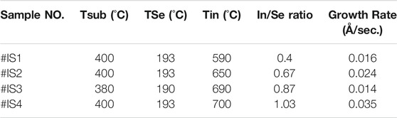
TABLE 1. Growth parameter list of InxSey.
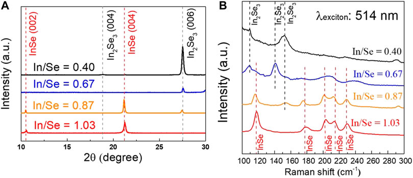
FIGURE 1. (A) XRD and (B) Raman spectra of InxSy with variation of In/Se ratio from 0,4 to 1.03, respectively.
The complex crystallographic orientation of the InxSey family makes phase control difficult. The experimental formation energy between InSe (−0.611 eV/atom) and In2Se3 (−0.572 eV/atom) is close, according to the open quantum materials database (Saal et al., 2013) (Kirklin et al., 2015). The phases of In2Se3 dominate when the amount of indium is deficient. Comparatively, multi-phases of InxSey, such as InSe, In2Se3 In4Se3 etc., would co-exist under indium rich conditions. In this study, we propose an innovative method for the growth of a single phase InSe thin film, alleviating the problem of the InSe-In2Se3 mixed crystal phase. This method is not only appropriate for growing on a lattice substrate, but is also valuable on an amorphous substrate. This method employs an indium precursor between the InSe epilayer and substrate. The concept and the detailed process can be summarized as: the indium precursor process is suitable when the substrate can be made sticky through indium deposition and can endure the subsequent growth temperature. The properties of the sticky coefficient and uniformity between the substrate and indium should be considered. Two substrates are used, sapphire and glass, to understand the advantage of this method. The experimental parameters are shown in Table 2. The excessive kinetic energy between the substrate and the dynamic indium molecular beam causes a poor sticky force when the amorphous substrate provides thermal energy, especially a glass substrate. Therefore, the substrate was held at room temperature (RT), to reduce the kinetic energy from the substrate surface, and rotated regularly during indium deposition (30 min). The indium molecular beam with a high cell temperature (830°C), i.e., high molecular flow, tends to stick to the substrate. After completing indium precursor deposition, the substrate is heated to 550°C; the solid indium precursor layer melts to a liquid state during this process. Following the indium precursor, a PVD InSe is deposited. The molecular beams of dynamic Se and In react with free-moving liquid indium, prioritizing the formation of a single-phase InSe thin film as a consequence. The thickness of InSe grown on glass (noted as #A1) is around 22 nm by high-resolution transmission electron microscopy (HRTEM). The growth periods are around 30 min for Indium-precursor and 30 min InSe growth. Therefore, the growth rate is around 0.73 nm/min. The growth period ratio of indium precursor and InSe is close to one in this case.
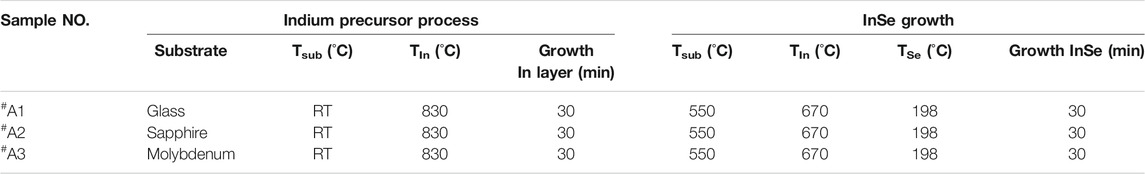
TABLE 2. Growth parameter list of InSe with indium precursor.
Figure 2 shows the Raman scattering of InSe grown on glass (#A1) and sapphire (#A2). A surprising discovery reveals that as the InSe growth was completed, the 2-inch molybdenum sample holder (#A3), as shown in Figure 2A, also exhibits InSe properties. The reason of similar Raman scattering results of sample #A1 to #A3 is that they are grown under the same growth mechanism. Indium is used as substrate adhesive. Therefore, the residual indium on the surface of molybdenum acts as a precursor for InSe growth. The Raman spectra of all three samples reveal characteristic modes of InSe. The excitation laser is set at 532 nm. These peaked at 116, 176, 201, and 228 cm−1, which correspond to the A1’ (Γ12), E' (Γ31)-TO/E'' (Γ33), A2'' (Γ11)-LO, and A1’ (Γ13) vibrational modes of InSe, respectively (Sorokin et al., 2020) (Mazumder et al., 2020) (Molas et al., 2021). These contributions are from out-of-phase vibrations of the In–Se bond within each vdW layer, as illustrated in Figure 2C. The weak shift with the samples is a change in the In–Se intralayer bonds. The results indicate that regardless of whether latticed or amorphous substrates, only a clear γ–InSe single-phase exists (Sorokin et al., 2020) (Mazumder et al., 2020) (Molas et al., 2021).
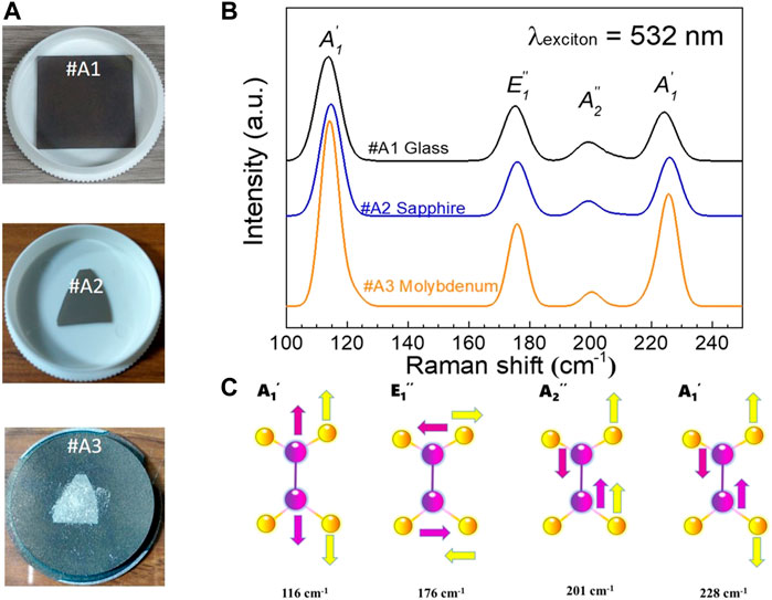
FIGURE 2. (A) shows a landscape of InSe growth on substrates of glass (#A1), sapphire (#A2), and molybdenum (#A3), respectively. The red ring mark is the measurement position of the Raman spectrum. (B) displays Raman spectra of samples #A1 to A3. (C) schematic the phonon vibration mode of InSe molecule at 116, 176, 201, and 228 cm−1, respectively.
Figures 3A,B illustrate high-resolution transmission electron microscopy images of samples #A1 and #A2, respectively, revealing the InSe/substrate interface landscape. InSe layers are ordered stacked by vdW force on either sapphire or glass, where monolayer thickness is around 0.8 nm. Both samples exhibit a depletion layer of precursor indium between the InSe and substrate (∼1.5 nm). It appears that the indium precursor layer has interacted with Se and In molecules, allowing an adequate penetration for the InSe growth. Most importantly, based on this growth method, the substrate selectivity regarding lattice mismatch seems to be inconsequential.
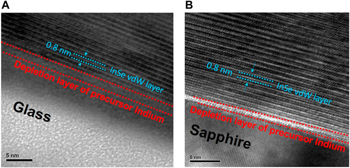
FIGURE 3. Cross-sectional TEM images of InSe films growth on (A) glass and (B) sapphire substrate. The vertically ordered InSe layers using weak van der Waals forces are clear found.
X-ray diffraction (XRD) has been carried out by a ω-2θ scan as shown in Figure 4 to investigate crystalline information. In Figure 4A, both samples exhibit clear InSe reflections of (003), (006), (009), and (0,018), respectively, referred to the ICSD data base (Muschinsky and Pawlenko, 1969). Take the (006) reflection, for example (Figure 4B), and compare the measurements of their features. The InSe thin film on the sapphire substrate has a narrower peak, as expected, due to a guiding lattice structure. However, although the glass substrate is amorphous, the InSe has grown on it also demonstrates surprising crystallinity. The lattice constant of both samples is almost the same when calculating the d-spacings. To further explore detailed information regarding the substrate effect on InSe thin film, the Williamson–Hall (W-H) plot is illustrated in Figure 4C. Comparing both fitted straight lines, using a sapphire substrate can result in an increased slope and lower y-intercept, attributed to the narrow peak width. Based on slope and y-intercept, the average crystalline size (D, nm), strain (ε × 10−3), and dislocation density (δ × 10−4, nm−2) has been estimated. The geometric parameters of the InSe thin films are recorded in Table 3. Calculations indicate that for InSe thin film growth, sapphire as a substrate h has a slightly higher strain and crystalline size than the glass substrate. There is a possibility that InSe may still be affected by the lattice substrate, where the lattice guides the InSe, resulting in a lower dislocation density. However, this growth method exhibits similar results even on the amorphous substrate. Admittedly, our growth method can obtain outstanding InSe vdW thin films using a glass substrate. Moreover, it demonstrates that substrate selection will not affect this growth mechanism, which will be competitive for future manufacturing device applications.
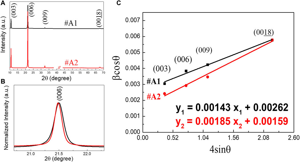
FIGURE 4. (A) shows the XRD spectra of InSe grown on glass and sapphire substrate. The reflection of InSe displays at (003), (006), (009), (0,018), respectively. (B) the XRD spectra zoomed in on (006) reflection. (C) W-H plots of βcosθ versus 4sinθ for #A1 and #A2.
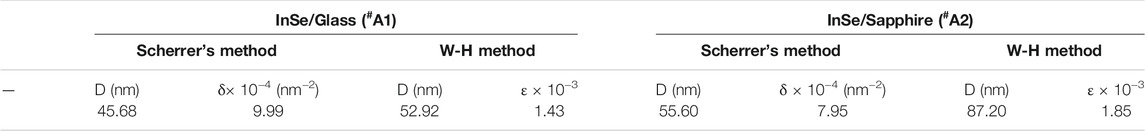
TABLE 3. Geometric parameters of InSe thin films.
Next, the #A1 sample was exposed to the atmosphere for 100 days to reveal its oxidation-related stability. Raman spectra in Figure 5A indicate no significant difference in the signals, exhibiting a high-quality lattice reliability. Therefore, SR-XPS was employed to investigate the chemical state and the electronic properties of the oxidation-related InSe at the surface. The core level spectra of In 3 days and Se 3d orbital are shown in Figures 5B,C. Quantitative analysis indicates the stoichiometric ratio of In and Se is 53: 47. The slight satellite signals near the higher binding energy of prominent peaks of the core level orbital can be detected, which is the contribution of InSe-oxidation, and it represents 5% of the total quantity of InSe surface (∼6 nm, estimated by XPS). The valence band spectrum in Figure 5D demonstrates that a signal onset at 1.21 eV binding energy below the Fermi-level is the valence band maximum. It is solely contributed by the Se 4p orbital edge (Guo and Robertson, 2017) rather than by oxygen from the atmosphere. The bandgap of bulk γ–InSe is around 1.28 eV. This result thus predicts n-type InSe. Despite being placed in an atmospheric environment for 100 days, the sample only shows 5% oxidation. Most importantly, the electronic properties of the InSe film are not affected at all by the atmosphere.
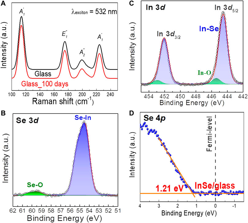
FIGURE 5. (A) Raman spectra of the InSe molecule before and after 100 days of atmospheric exposure (B–D) display XPS measurements after 100 days of atmospheric exposure (B) Se 3 days and (C) In 3 days core level orbitals of InSe show that only 5% oxidation within the InSe surface (D) shows valence band spectra of InSe after atmospheric exposure.
The defective InSe by Se vacancies or edge sites can change its energy formation (Boukhvalov et al., 2017) (Politano et al., 2016). The catalytic processes of InSe with ambient gases in the atmosphere will occur, which can induce the surface reactivity regarding hydrogen evolution reaction (HER) and oxygen evolution reaction (OER) (D’Olimpio et al., 2020). Those reaction activities can increase with decrease the thickness of InSe. Especially, the thickness closes to atomic scale. Furthermore, the electronic band structure of InSe flake with selenium vacancies is affected by atmospheric gases (Politano et al., 2017) (Boukhvalov et al., 2017), which is an opportunity to form a p-type in device character (Boukhvalov et al., 2017) (Politano et al., 2016). Our growth method can offer InSe with less defect density, which benefits the discussion for subsequent manufacturing of the device, clarifying the state of surface control.
In general, the growth of MBE is based on thermodynamic equilibrium. The surface lattices of substrates obtain thermal energy, causing the phonon resonance which is the anharmonic effect of lattice dynamics (Katsnelson, 2005), thereby generating kinetic energy that guides the coupling of dynamic molecular beam atoms. According to the Frank–van der Merwe growth mechanism, this process ideally would result in three key issues: the chemical bonding between atoms in a monolayer, the arrangement of small atomic displacements, and the layer-by-layer growth of a vdW thin film.
Due to the approximative compound-formation-energies of InSe and In2Se3, it is arduous to efficiently select a single crystalline phase of the film during epitaxy. The In2Se3 crystalline dominates under poor indium conditions. Hence, it is essential to ensure that the indium is stable and sufficient for reaction during InSe growth. According to the experience from CuInGaSe2 semiconductor, indium is a soft and malleable element which has a low melting point (156.60°C) and an excellent diffusion ability in the CIGS system during thermal process (Djessas et al., 2004) (Muzzillo et al., 2016). Indium is also commonly used in abrupt ion-implantation and has been applied to MOSFETs (Suzuki et al., 1999). Therefore, based on these experiences, using the liquid indium precursor layer, the properties of free-moving of dislocations (Ziman, 1972), forces the priority formation of the InSe phase during the growth process. Figure 6 illustrates the growth flow of this method. This innovative growth method overcomes the weakness of the lack of indium in the growth process of InSe (Figure 6B). Furthermore, the chemical bonding of two-dimensional vdW materials exists only in the monolayer, as well as the layer-to-layer is vdW forces. We speculate that the anharmonic effect of lattice substrates is beneficial in reducing the dislocation density and increasing the crystalline size. However, the results of this study imply that may not be necessary. Since the inherent anharmonic effect of honeycomb lattice InSe cooperates with the vdW forces’ dependency on layer stacking, this leads to coupling and orderly arranging by self-assembly interaction between the formed InSe molecules in the liquid indium environment (Figure 6C). Thus, those molecules can be easily placed in an orderly fashion on amorphous substrates. It also explains why the substrate type is not critical in our experiments.
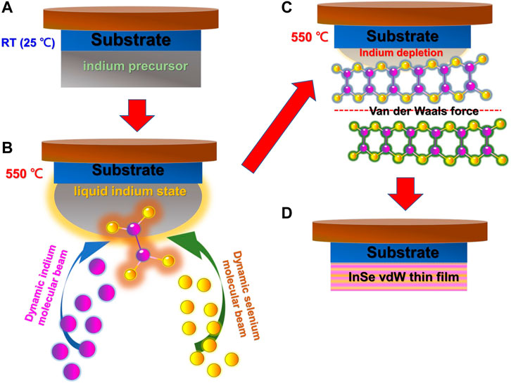
FIGURE 6. schematics the mechanism of InSe growth flow with indium precursor method. (A) represents the deposition of indium precursor on substrate. (B) represents formation of InSe molecule assisted by liquid indium bank. (C) represents InSe layer of molecule self-assembly based on anharmonic properties and van der Waals force. (D) represents the formation of InSe vdW thin film.
Flexibility is an important characteristic of vdW thin film. Therefore, it is important to demonstrate the vdW thin film on a flexible substrate. An InSe vdW thin film has been successfully grown on a soft aluminum foil substrate using this novel method. Figure 7A shows a landscape of InSe growth on an aluminum substrate. The red ring mark is the measurement position of the Raman spectrum. Figure 7B schematic the diagram of InSe stacked on the aluminum substrate. Figure 7C displays the Raman spectrum of this sample. The Raman spectrum is similar to the previous one. The reliable InSe vdW thin film from this innovation growth method proves that the growth is not limited to substrates. It combines the growth mechanism of the indium precursor layer and InSe vdW layer, thus exhibiting the potential for device manufacturing applications in the future.
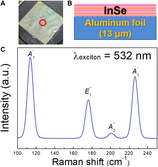
FIGURE 7. shows the growth of InSe with indium precursor on the flexible substrate. (A) shows a landscape of InSe growth on an aluminum substrate. The red ring mark is the measurement position of the Raman spectrum. (B) schematic the diagram of InSe stacked on the aluminum substrate. (C) displays the Raman spectrum of InSe/aluminum substrate.
Conclusion
In this study, we demonstrate a novel InSe growth method using MBE to address the problem regarding In2Se3-InSe phase coexistence in the vdW thin film. The indium precursor was employed to guide the phase transition due to the lack of indium during the epitaxy growth, resulting in a pure InSe phase. This method allows for a wider choice of substrates, which benefits from the character of the indium precursor layer and anharmonic lattice of InSe. During growth, free-moving liquid indium can participate in the formation of InSe molecules. Furthermore, the anharmonic lattice of InSe can vertically order layers using weak van der Waals forces. This method is an innovative and forward-looking approach to developing 2D InSe electric devices in the future.
Data Availability Statement
The original contributions presented in the study are included in the article/Supplementary Material, further inquiries can be directed to the corresponding authors.
Author Contributions
This work is collaborating with these nine authors. The idea comes from C-SY and S-WH. All experiments were done by S-WH, H-NY, C-HW, S-KW, L-YC, and Y-TH. Data analysis was done by C-SY, S-WH, Y-TH, S-JC, and W-CC. The manuscript was written by S-WH and C-SY.
Conflict of Interest
The authors declare that the research was conducted in the absence of any commercial or financial relationships that could be construed as a potential conflict of interest.
Publisher’s Note
All claims expressed in this article are solely those of the authors and do not necessarily represent those of their affiliated organizations, or those of the publisher, the editors and the reviewers. Any product that may be evaluated in this article, or claim that may be made by its manufacturer, is not guaranteed or endorsed by the publisher.
Acknowledgments
The authors would like to thank the foundation support by Tatung University and the financial supported by the “Center for the Semiconductor Technology Research” from the Ministry of Education (MOE) in Taiwan, as well as supported in part by the Ministry of Science and Technology, Taiwan, under Grant MOST 110–2634-F-009-027 and 109-2124-M-009-002-MY3. Additionally, we appreciate Dr-Ing. Eric Koenig, who is faculty at the Applied Mathematics, Physics, and Humanities of Technische Hochschule Nürnberg, for the correction of English writing.
References
Balakrishnan, N., Kudrynskyi, Z. R., Fay, M. W., Mudd, G. W., Svatek, S. A., Makarovsky, O., et al. (2014). Room Temperature Electroluminescence from Mechanically Formed van der Waals III-VI Homojunctions and Heterojunctions. Adv. Opt. Mater. 2, 1064–1069. doi:10.1002/adom.201400202
Bandurin, D. A., Tyurnina, A. V., Yu, G. L., Mishchenko, A., Zólyomi, V., Morozov, S. V., et al. (2017). High Electron Mobility, Quantum Hall Effect and Anomalous Optical Response in Atomically Thin InSe. Nat. Nanotech 12, 223–227. doi:10.1038/nnano.2016.242
Bonaccorso, F., Sun, Z., Hasan, T., and Ferrari, A. C. (2010). Graphene Photonics and Optoelectronics. Nat. Photon 4, 611–622. doi:10.1038/nphoton.2010.186
Boukhvalov, D., Gürbulak, B., Duman, S., Wang, L., Politano, A., Caputi, L., et al. (2017). The Advent of Indium Selenide: Synthesis, Electronic Properties, Ambient Stability and Applications. Nanomaterials 7, 372–416. doi:10.3390/nano7110372
Brotons-Gisbert, M., Andres-Penares, D., Suh, J., Hidalgo, F., Abargues, R., Rodríguez-Cantó, P. J., et al. (2016). Nanotexturing to Enhance Photoluminescent Response of Atomically Thin Indium Selenide with Highly Tunable Band Gap. Nano Lett. 16, 3221–3229. doi:10.1021/acs.nanolett.6b00689
Buscema, M., Island, J. O., Groenendijk, D. J., Blanter, S. I., Steele, G. A., van der Zant, H. S. J., et al. (2015). Photocurrent generation with two-dimensional van der Waals semiconductors. Chem. Soc. Rev. 44, 3691–3718. doi:10.1039/c5cs00106d
Cai, H., Gu, Y., Lin, Y.-C., Yu, Y., Geohegan, D. B., and Xiao, K. (2019). Synthesis and Emerging Properties of 2D Layered III-VI Metal Chalcogenides. Appl. Phys. Rev. 6, 041312. doi:10.1063/1.5123487
Chatillon, C., and Emery, J.-Y. (1993). Thermodynamic Analysis of Molecular Beam Epitaxy of Compounds in the In-Se System. J. Cryst. Growth 129, 312–320. doi:10.1016/0022-0248(93)90462-6
Chevy, A. (1984). Improvement of Growth Parameters for Bridgman-grown InSe Crystals. J. Cryst. Growth 67, 119–124. doi:10.1016/0022-0248(84)90140-4
Chierchia, R., Böttcher, T., Heinke, H., Einfeldt, S., Figge, S., and Hommel, D. (2003). Microstructure of Heteroepitaxial GaN Revealed by X-ray Diffraction. J. Appl. Phys. 93, 8918–8925. doi:10.1063/1.1571217
Curreli, N., Serri, M., Spirito, D., Lago, E., Petroni, E., Martín‐García, B., et al. (2020). Liquid Phase Exfoliated Indium Selenide Based Highly Sensitive Photodetectors. Adv. Funct. Mater. 30, 1908427–1908510. doi:10.1002/adfm.201908427
D'Olimpio, G., Nappini, S., Vorokhta, M., Lozzi, L., Genuzio, F., Menteş, T. O., et al. (2020). Enhanced Electrocatalytic Activity in GaSe and InSe Nanosheets: The Role of Surface Oxides. Adv. Funct. Mater. 30, 2005466–2005511. doi:10.1002/adfm.202005466
Djessas, K., Yapi, S., Massé, G., Ibannain, M., and Gauffier, J. L. (2004). Diffusion of Cu, in, and Ga in In2Se3/CuGaSe2/SnO2 Thin Film Photovoltaic Structures. J. Appl. Phys. 95, 4111–4116. doi:10.1063/1.1652252
Fang, H., Chuang, S., Chang, T. C., Takei, K., Takahashi, T., and Javey, A. (2012). High-Performance Single Layered WSe2 P-FETs with Chemically Doped Contacts. Nano Lett. 12, 3788–3792. doi:10.1021/nl301702r
Gomes Da Costa, P., Dandrea, R. G., Wallis, R. F., and Balkanski, M. (1993). First-principles Study of the Electronic Structure of γ-InSe and β-InSe. Phys. Rev. B 48, 14135–14141. doi:10.1103/PhysRevB.48.14135
Groot, C. H. D., and Moodera, J. S. (2001). Growth and Characterization of a Novel In2Se3 Structure. J. Appl. Phys. 89, 4336–4340. doi:10.1063/1.1355287
Guo, Y., and Robertson, J. (2017). Band Structure, Band Offsets, Substitutional Doping, and Schottky Barriers of Bulk and Monolayer InSe. Phys. Rev. Mater. 1, 1–9. doi:10.1103/PhysRevMaterials.1.044004
Han, G., Chen, Z.-G., Drennan, J., and Zou, J. (2014). Indium Selenides: Structural Characteristics, Synthesis and Their Thermoelectric Performances. Small 10, 2747–2765. doi:10.1002/smll.201400104
Hao, Q., Yi, H., Su, H., Wei, B., Wang, Z., Lao, Z., et al. (2019). Phase Identification and Strong Second Harmonic Generation in Pure ε-InSe and its Alloys. Nano Lett. 19, 2634–2640. doi:10.1021/acs.nanolett.9b00487
Hayashi, T., Ueno, K., Saiki, K., and Koma, A. (2000). Investigation of the Growth Mechanism of an InSe Epitaxial Layer on a MoS2 Substrate. J. Cryst. Growth 219, 115–122. doi:10.1016/S0022-0248(00)00627-8
Heryanto, H., Abdullah, B., Tahir, D., and Mahdalia, (2019). Quantitative Analysis of X-Ray Diffraction Spectra for Determine Structural Properties and Deformation Energy of Al, Cu and Si. J. Phys. Conf. Ser. 1317, 012052–12111. doi:10.1088/1742-6596/1317/1/012052
Hsiao-Yuan Huang, C.-S. Y. (2011). Growth and Characterization of CuInSe 2 Thin Film Solar Cells by Plasma-Assisted Molecular Beam Epitaxy. Taipei: Thesis for Master of Science Graduate Institute of Electro-optical engineering Tatung University. Thesis.
Huang, W., Gan, L., Li, H., Ma, Y., and Zhai, T. (2016). 2D Layered Group IIIA Metal Chalcogenides: Synthesis, Properties and Applications in Electronics and Optoelectronics. CrystEngComm 18, 3968–3984. doi:10.1039/c5ce01986a
Jiang, J., Li, J., Li, Y., Duan, J., Li, L., Tian, Y., et al. (2019). Stable InSe Transistors with High-Field Effect Mobility for Reliable Nerve Signal Sensing. Npj 2d Mater. Appl. 3, 1. doi:10.1038/s41699-019-0110-x
Katsnelson, M. I. (2005). Lattice Dynamics: Anharmonic Effects. Encycl. Condens. Matter Phys., 84 77–82. doi:10.1016/B0-12-369401-9/00512-X
Kim, S., Konar, A., Hwang, W.-S., Lee, J. H., Lee, J., Yang, J., et al. (2012). High-mobility and Low-Power Thin-Film Transistors Based on Multilayer MoS2 Crystals. Nat. Commun. 3, 1011–1018. doi:10.1038/ncomms2018
Kirklin, S., Saal, J. E., Meredig, B., Thompson, A., Doak, J. W., Aykol, M., et al. (2015). The Open Quantum Materials Database (OQMD): Assessing the Accuracy of DFT Formation Energies. Npj Comput. Mater. 1, 15010–15024. doi:10.1038/npjcompumats.2015.10
Levi, A. C., and Kotrla, M. (1997). Theory and Simulation of crystal Growth. J. Phys. Condens. Matter 9, 299–344. doi:10.1088/0953-8984/9/2/001
Lewandowska, R., Bacewicz, R., Filipowicz, J., and Paszkowicz, W. (2001). Raman Scattering in α-In2Se3 Crystals. Mater. Res. Bull. 36, 2577–2583. doi:10.1016/s0025-5408(01)00746-2
Liu, X., Ren, J.-C., Shen, T., Li, S., and Liu, W. (2019). Lateral InSe P-N Junction Formed by Partial Doping for Use in Ultrathin Flexible Solar Cells. J. Phys. Chem. Lett. 10, 7712–7718. doi:10.1021/acs.jpclett.9b03184
Mazumder, D., Xie, J., Kudrynskyi, Z. R., Wang, X., Makarovsky, O., Bhuiyan, M. A., et al. (2020). Enhanced Optical Emission from 2D InSe Bent onto Si‐Pillars. Adv. Opt. Mater. 8, 2000828. doi:10.1002/adom.202000828
Molas, M. R., Tyurnina, A. V., Zólyomi, V., Ott, A. K., Terry, D. J., Hamer, M. J., et al. (2021). Raman Spectroscopy of GaSe and InSe post-transition Metal Chalcogenides Layers. Faraday Discuss. 227, 163–170. doi:10.1039/d0fd00007h
Mortelmans, W., De Gendt, S., Heyns, M., and Merckling, C. (2021). Epitaxy of 2D chalcogenides: Aspects and consequences of weak van der Waals coupling. Appl. Mater. Today 22, 100975. doi:10.1016/j.apmt.2021.100975
Mote, V., Purushotham, Y., and Dole, B. (2012). Williamson-hall Analysis in Estimation of Lattice Strain in Nanometer-Sized ZnO Particles. J. Theor. Appl. Phys. 6, 6–13. doi:10.1186/2251-7235-6-6
Muschinsky, W. P., and Pawlenko, N. M. (1969). Untersuchung des Systems GaSe-InSe. Crystal Research and Technology 4 (2), K5–K7. doi:10.1002/crat.19690040217
Muzzillo, C. P., Campbell, C. E., and Anderson, T. J. (2016). Cu-Ga-In Thermodynamics: Experimental Study, Modeling, and Implications for Photovoltaics. J. Mater. Sci. 51, 3362–3379. doi:10.1007/s10853-015-9651-3
Politano, A., Campi, D., Cattelan, M., Ben Amara, I., Jaziri, S., Mazzotti, A., et al. (2017). Indium Selenide: An Insight into Electronic Band Structure and Surface Excitations. Sci. Rep. 7, 1–11. doi:10.1038/s41598-017-03186-x
Politano, A., Chiarello, G., Samnakay, R., Liu, G., Gürbulak, B., Duman, S., et al. (2016). The Influence of Chemical Reactivity of Surface Defects on Ambient-Stable InSe-Based Nanodevices. Nanoscale 8, 8474–8479. doi:10.1039/c6nr01262k
Rabiei, M., Palevicius, A., Monshi, A., Nasiri, S., Vilkauskas, A., and Janusas, G. (2020). Comparing Methods for Calculating Nano crystal Size of Natural Hydroxyapatite Using X-ray Diffraction. Nanomaterials 10, 1627–1721. doi:10.3390/nano10091627
Saal, J. E., Kirklin, S., Aykol, M., Meredig, B., and Wolverton, C. (2013). Materials Design and Discovery with High-Throughput Density Functional Theory: The Open Quantum Materials Database (OQMD). Jom 65, 1501–1509. doi:10.1007/s11837-013-0755-4
Sorokin, S. V., Avdienko, P. S., Sedova, I. V., Kirilenko, D. A., Davydov, V. Y., Komkov, O. S., et al. (2020). Molecular Beam Epitaxy of Layered Group III Metal Chalcogenides on GaAs(001) Substrates. Materials 13, 3447. doi:10.3390/MA13163447
Suzuki, K., Tashiro, H., and Aoyama, T. (1999). Diffusion Coefficient of Indium in Si Substrates and Analytical Redistribution Profile Model. Solid-State Elect. 43, 27–31. doi:10.1016/S0038-1101(98)00251-2
Weszka, J., Daniel, P., Burian, A., Burian, A. M., and Nguyen, A. T. (2000). Raman Scattering in In2Se3 and InSe2 Amorphous Films. J. Non-Crystalline Sol. 265, 98–104. doi:10.1016/S0022-3093(99)00710-3
Yang, Z., and Hao, J. (2019). Recent Progress in 2D Layered III-VI Semiconductors and Their Heterostructures for Optoelectronic Device Applications. Adv. Mater. Technol. 4, 1900108–1900124. doi:10.1002/admt.201900108
Zeng, Z., Li, S., Tadano, T., and Chen, Y. (2020). Anharmonic Lattice Dynamics and thermal Transport of Monolayer InSe under Equibiaxial Tensile Strains. J. Phys. Condens. Matter 32, 475702. doi:10.1088/1361-648X/aba315
Zhang, L., Li, Z., Liu, J., Peng, Z., Zhou, J., Zhang, H., et al. (2020). Optoelectronic Gas Sensor Based on Few-Layered InSe Nanosheets for NO2 Detection with Ultrahigh Antihumidity Ability. Anal. Chem. 92, 11277–11287. doi:10.1021/acs.analchem.0c01941
Ziman, J. M. (1972). Principles of the Theory of Solids. 2nd ed. Cambridge: Cambridge University Press. doi:10.1017/CBO9781139644075
Keywords: 2D materials, indium precursor layer, molecular beam epitaxy, Raman scattering spectrum, x-ray diffraction
Citation: Hsiao S-W, Yang C-S, Yang H-N, Wu C-H, Wu S-K, Chang L-Y, Ho Y-T, Chang S-J and Chou W-C (2022) Novel Method for the Growth of Two-Dimensional Layered InSe Thin Films on Amorphous Substrate by Molecular Beam Epitaxy. Front. Mater. 9:871003. doi: 10.3389/fmats.2022.871003
Received: 07 February 2022; Accepted: 25 February 2022;
Published: 23 March 2022.
Edited by:
Antonio Politano, University of L'Aquila, ItalyReviewed by:
Yen-Fu Lin, National Chung Hsing University, TaiwanChiu-Yen Wang, National Taiwan University of Science and Technology, Taiwan
Copyright © 2022 Hsiao, Yang, Yang, Wu, Wu, Chang, Ho, Chang and Chou. This is an open-access article distributed under the terms of the Creative Commons Attribution License (CC BY). The use, distribution or reproduction in other forums is permitted, provided the original author(s) and the copyright owner(s) are credited and that the original publication in this journal is cited, in accordance with accepted academic practice. No use, distribution or reproduction is permitted which does not comply with these terms.
*Correspondence: Chu-Shou Yang, Y3N5YW5nQGdtLnR0dS5lZHUudHc=; Wu-Ching Chou, d2NjaG91OTU3QG55Y3UuZWR1LnR3