- 1School of Chemical and Materials Engineering (SCME), National University of Sciences and Technology (NUST), Islamabad, Pakistan
- 2Department of Physics, International Islamic University Islamabad, Islamabad, Pakistan
- 3Thin Films Technology Research Laboratory COMSATS University (CUI) Islamabad, Islamabad, Pakistan
Zinc oxide/carbon nanotube (ZnO/CNTs) nanocomposites are developed on gold (Au)-coated unpolished Si p-type (100) substrates with 2, 4, 6, 8, and 10 nm thicknesses by vapor–liquid–solid method. One set of Au-coated Si substrates are annealed to develop Si–Au samples for better nucleation. XRD, FE-SEM, Raman, and photoluminescence spectroscopic characterizations are used to study structural, morphological, and optical properties on annealed and unannealed catalyst layers with various Au thickness samples. In XRD results, the ZnO/CNT nanocomposites are observed with higher crystallinity and purity of phase. FE-SEM images showed variety of nanostructures with variation in morphologies with respect to Au thickness in annealed and unannealed samples. Clear indication of high defect concentrations and high crystallinity is observed in Raman spectra. It is observed in PL spectra that preferred peak orientation with shift ∼4 nm in the unannealed Au layer and ∼9 nm in annealed Au layer samples exhibited formation of ZnO/CNT nanocomposites. Efficient sensing is observed in the 6-nm thickness Au layer in the unannealed sample. Annealed Au-coated Si samples at 8 and 10 nm thicknesses showed efficient UV sensing with quick response and recovery time.
1 Introduction
ZnO nanostructures have a wide range of operating temperature, stability, and flexibility, which make them a good candidate for sensing applications (Sinha et al., 2006; Yin et al., 2013). Keeping in view the properties and sensing results of ZnO- and CNT-based sensors, nanocomposites are designed for sensing applications. Different ZnO morphologies have different sensing responses. The effective sensing applications of nanocomposites must have some properties such as high surface area, high crystallinity, and organized molecular structure. ZnO exhibits conductivity in the presence of UV light, as reported earlier (Comini, 2009; Tiwari et al., 2012). This variation in electronic conductivity is exploited in UV photodetectors and photoswitches. CNTs increase the conductivity of ZnO-based nanocomposites, which results in quick recovery and response time (Xia et al., 2003). Various methods are used for the synthesis of nanostructures such as the liquid phase technique, vapor phase technique (Xu, 2005), spray pyrolysis (Sadananda Kumar et al., 2014), electrochemical technique (Wong, 2003; Amin, 2015), and chemical precipitation. The vapor phase technique is the recommended technique for the controlled growth of nanostructures due to the vapor–liquid–Solid (VLS) and vapor–solid (VS) growth mechanisms (Choi et al., 2002; Amin et al., 2014). VLS is a cost-effective and easy-to-handle method to generate single crystalline one-dimensional nanostructures (Chen et al., 2013). Mostly commercial sensors are less cost-effective, bulky, offer complex designing, or involve time-consuming methods to start the effective functioning of devices. To overcome the shortcomings of commercially available sensors, scientists start to exploit nanostructures and nanoparticles (HullavaradHullavarad et al., 2009).
Metal oxides are the effective sensing materials as anions are usually available with vacancies whereas cations exist with mixed valence states in them. Alteration in properties of oxide semiconductors offers tailoring of the optical band gap, electrical, chemical, and magnetic properties, which enable scientists to develop more efficient devices. Zinc oxide (ZnO) is an effective material for sensing devices (Wan et al., 2004; Bai et al., 2011) for both chemicals (Carotta et al., 2009) and UV radiations (Hierold, 2009; Zhai et al., 2009). Sensing is a very sensitive process; it involves the manufacture of a pure crystalline state and high-quality nanostructures. ZnO allows variety of nanostructures with wider band gaps (3.37 eV at room temperature) (Lee et al., 2009) that are suitable for sensing applications (Zhang et al., 2010). The unique quality of surface polarity and surface plane energies in ZnO allows synthesis of diverse morphologies (Givargizov, 1975). ZnO also have strong piezoelectric and optical properties which make it a more interesting material for sensing applications.
Carbon nanotubes (CNTs) can alter their electrical properties upon interacting with molecules in the nearby environment (Li et al., 2003). CNTs have drastically different mechanical, electrical, optical, and electromechanical properties, which give researchers the urge to experiment with them and discover their applications at the nanoscale. They provide highly selective, responsive, cheap, and sensitive sensors depending upon their structures (JohanssonWacaser et al., 2006; Wang et al., 2008). Combined effects of CNTs and ZnO exhibit amazing properties in nanocomposites, such as high current flow (1.1 mA) at low voltage (1Volt) and increased optical transmittance (70–80%). Compared to CNTs, ZnO nanostructures show enhanced divergent light emission with optical transition and mechanical properties (Wang and Geng, 2005). These changes in properties give insights about next-generation applications in optoelectronic and electronic fields such as batteries, solar cells, supercapacitors, and sensors. (Wang, 2003).
ZnO and CNT nanocomposites are reported to have enhanced UV and visible ranges because of their defects. Mechanical properties of CNTs combine with ZnO results in enhancement of mechanical strength of ZnO nanostructures. ZnO shows structural defects in the basal plane while forming nanocomposites with CNTs. These defects in ZnO allow monochromatic emission in the UV range i.e., 373–376 nm (Roper et al., 2007). This low level emission increases the chances of electron-hole recombination. Nanocomposites of such ZnO nanostructures and CNTs show stability-enhanced mechanical, electrical, magnetic, and optical behaviors which allow these nanocomposite potential applications (Wang, 2009), such as photocatalysts (Afrin et al., 2013), nanoelectronics, nanodevices, and sensors. The literature studies have reported to form various ZnO/CNT nanocomposite methods such as hydrothermal methods (Nasser, 2020), wet-chemical method (Vyas et al., 2012), sol–gel method (Albiss et al., 2010; Ahmed Jamal et al., 2017), layer-by-layer (LBL) self-assembly technique for thin film formation (Hernández, 2012), electrochemical synthesis method (Zhang et al., 2009), thermal decomposition method (Khanderi et al., 2009), chemical reflux method (Ranjithkumar et al., 2019), and simple/efficient ultrasonic-based method (Farbod et al., 2016; Subodh, 2017a; Subodh, 2017b). No literature has reported the direct synthesis of ZnO nanostructures over the CNTs.
The method used in this study develops a direct link between the CNTs and ZnO nanostructures during synthesis. It is the major factor of increased response time of sensors. The VLS method can be further exploited for numerous applications of gas and electrochemical sensing and photocatalytic activity. This work is motivated by the unique properties of CNTs and ZnO provoking to develop nanocomposites to utilize both material properties to generate effective sensors. The VLS method is used for the growth of ZnO nanostructures at different thicknesses of the catalyst layer. The effect of annealing of the catalyst layer is considered in this study as it affects the properties of nanostructures drastically. It also helps to better understand composite properties. The properties of prepared samples are studied by X-ray diffraction, field emission scanning electron microscopy, photoluminescence, and Raman spectroscopy. The sensors are developed for UV sensing. Numerous nanostructures of ZnO are used to form nanocomposites with CNTs to develop quick responsive sensors. The inert nature of ZnO is very suitable for the environment despite being at the nanolevel. Very encouraging results with high sensitivity and quick response time of UV sensors are reported in this study.
2 Experimental Methods
2.1 Growth of ZnO Nanostructure by the VLS Method
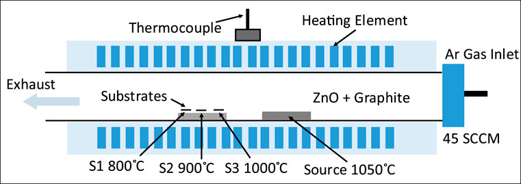
For the study, 1 g of the prepared source was placed in a ceramic boat; then, the boat was pushed precisely at the center of a quartz tube with 100 cm length and 3.5 cm diameter (Lao et al., 2003). The processed substrate was placed on another ceramic boat with the help of a carbon tape. It will provide a heating path to the substrate and allow the substrates to stick to the defined position during the experiment. The substrate-holding boat was pushed adjacent to the source boat in the quartz tube. The tube with both boats was placed in an electric furnace (local electric furnace) with care. Argon (Ar) gas was supplied by connecting the quartz tube cap, while the other end was kept open. Ar gas was allowed to flow at 45 SCCM (standard cubic centimeters per minute) through the tube, prior to the start of the furnace to avoid impurities. The furnace was programmable at 1050°C, while the gas flow was maintained at 45 SCCM. The rise of temperature in the furnace was 10°C per minute. Ar gas was used as a carrier gas of ZnO vapors to Au-coated Si substrates. The systematic experimental set up is shown in Figure 1.
The VLS method is used for the growth of ZnO nanostructures at different thicknesses of the catalyst layer. VLS growth is a nucleation-based growth; as shown in Figure 2, mostly metal catalysts are used for this purpose. Usually nuclei are formed by the mixing of catalyst and source vapors during synthesis. If the nuclei are formed during an internal chemical reaction, then the process is called self-catalyzed VLS growth. A suitable additive material within the source can reasonably reduce its vaporization temperature. ZnO have a vaporization temperature up to 1,900°C which can be reduced approximately up to 1,000°C by adding graphite (C) powder with ZnO. The fine mixture of graphite in ZnO leads to the development of Zn or Zn sub-oxide vapors at 1000°C due to the following chemical reaction (Djurišić and Leung, 2006).
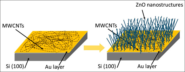
FIGURE 2. Schematic diagram of CNTs deposited on the Au layer and growth of ZnO nanostructures by the VLS method.
The forms of nanostructures are dependent on Zn and Zn sub-oxides at lower temperatures since Zn oxides play a major role in the nucleation of ZnO nanostructures, while the other parameters such as vacuum condition, carrier gases, and catalyst become less influential on the nanostructures. Hence, the principal effecting parameter for ZnO growth of nanostructures is temperature (Kim and Sigmund, 2002). There is a possibility of direct reaction of the graphite powder with ZnO vapors or oxygen (O) present in the tube, resulting in carbon monoxide (CO) gas. Such a reaction depends upon the atmospheric conditions of the tube. In an open-ended quartz tube, vapors of sub-oxides of Zn generate at low temperature due to mixing of the graphite powder. Partial oxidation of Zn occurs due to the lack of oxygen (O) in the open-ended tube during synthesis of nanostructures. The droplets are generated by the vaporization of ZnO and its sub-oxides, which act as nuclei for 1-D growth of ZnO nanostructures. Zn sub-oxides are unstable compounds, so their electron affinity is not completely satisfied as in ZnO. This reactive nature of Zn sub-oxides is responsible to increase the growth of the ZnO nanostructure at the tips, resulting in the micro length of 1-D nanostructures, as shown in Figure 3. Higher surface tension, wetting ability, and higher accommodation coefficients make Au an extensively used catalyst for the growth of the 1-D nanostructure (Li et al., 2010). Au supports highly crystalline, dense, long, and manageable diameter of nanostructures as the catalyst. 1-D nanostructures using Au catalysts, showing high crystallinity and density, are reported in the literature (Zhang et al., 2010).
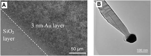
FIGURE 3. (A) SEM image of Au and SiO2 junction, (B) TEM image of the ZnS nanobelt with Au catalyst at the tip of the nanostructure (Zhang et al., 2010).
In the VLS method, the position of the substrate needs to be optimized for particular morphology of the nanostructure of the source material. Vapor pressure and temperature vary every cm within the synthesis tube with respect to the source. The tube furnace is open from both sides, which creates a major difference in the temperature with distance from the center. Different planes have different activation energies, which create different morphologies within the tube. Second, vapor pressure varies with distance, resulting in the difference of supersaturation of droplets. These phenomenal changes in the precipitation rate of droplets eventually affect the morphology of the nanostructure.
2.2 UV-Sensing Mechanism
The principle of UV-sensing mechanism is photoconductivity. Oxygen defects have a major influence on electrical properties and on the optical band structure (Wen et al., 2012). ZnO nanostructures synthesized by the VLS method have oxygen defects and point defects which enable good sensing response and recovery time. Oxygen vacancies in the ZnO nanostructure are due to Zn oxide and sub oxides which can be increased by post-annealing in the oxygen environment. Introduction of oxygen vacancies creates a blue shift in the luminescence spectrum. ZnO creates a bond with the CNTs sp2 surface and shows high permeability for air (Zhu et al., 2009). The rough surface of the nanostructure offers an increased adsorption of oxygen which enhances the response of sensors (Kim, 2009).
Oxygen adsorbed on the surface is responsible for photosensitivity (Guo, 2010). In the absence of UV light, oxygen molecules adsorb on the outer surface of ZnO and remove free electrons which create a depletion region; as a result, it reduces conduction in the sensor (Fu et al., 2012), as shown in Figure 4.

FIGURE 4. Schematic of (A) UV sensor (B) photo response mechanism in dark (C) photo response in UV light. (D) Energy band diagram of the photo response process during UV-sensing.
The reaction that occurs during UV-sensing in dark is given below:
In the presence of UV light, absorption of photons creates electron-hole pairs which flow through the depletion region. A sudden increase of the current is observed, while +holes are attracted to the O−2 ion to neutralize the ion in the oxygen molecule. The release of the oxygen molecule from the surface causes a change in the surface reaction.
As holes neutralize with oxygen ions, they leave electrons of their pairs free to conduct photoelectricity in nanocomposites. Delay in the response and recovery time happens if electrons get trapped in deep defects on the surface of ZnO nanostructures or CNTs. These traps hinder electron recombination and increase hole duration in the electronic band (Ali and Chakrabarti, 2010).
2.3 Annealing of Au-Coated Si Substrates
One set of Au-coated Si substrates with 2 nm, 4 nm, 6 nm, 8 nm, and 10 nm thicknesses were annealed in a furnace (Protherm laboratory furnaces MOS 160/2) at 250°C for 2 h in air. This heat treatment allows the Au atoms to penetrate in the Si wafer, leading to a good Si–Au system which causes better nucleation for the VLS growth of nanostructures (Amin et al., 2012). The Si–Au system was developed in an excessive oxygen (O2) environment. Due to the presence of O2, there is a formation of Si oxides (SiO, SiO2). It is supportive for rich branched ZnO nanostructures providing wider areas for sensing applications. The process enhances the formation of nanocomposites of ZnO and CNTs.
2.4 Preparation of CNT Suspension
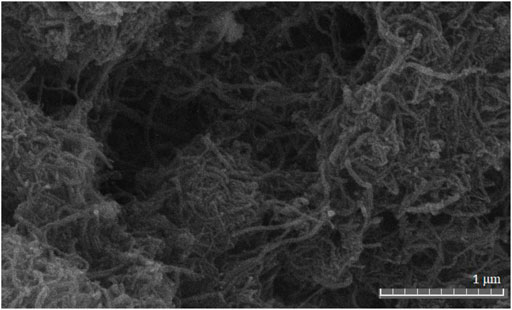
Pristine multi-walled carbon nanotubes MWCNTs with length approximately 10–20 µm and diameter approximately 25–60 nm with 95% purity were purchased from Beijing DK nanotechnology (China). MWCNTs have lesser than 4% amorphous carbon and approximately 0.5% metal impurity. MWCNTs, as shown in Figure 5, were used without any treatment for synthesis of ZnO/CNT nanocomposites. CNT suspension was prepared by dissolving 200 mg of MWCNTs in 5 ml of 95% acetone (C3H6O). The obtained suspension was sonicated for 20 min in an ultrasonic sonicator. MWCNTs were deposited on Au-coated Si wafers by the drop-casting method. For the experiment, 50 µL suspensions was taken in a micropipette and poured on each sample of both sets.
After drying at room temperature, 50 µL suspensions were again poured on the samples. The process was repeated thrice. The mixture of graphite powder and ZnO was used as the source instead of ZnO because this mixture helps to lower the evaporation temperature of ZnO from 1975 to 600°C. It is a well-known fact; the graphite powder is a good conductor of heat and electricity which is used to lower the evaporation temperature of ZnO. The localized heating of ZnO atoms was performed by using fine graphite powder. The process was aggravated by mixing both compounds with ball milling, which helps to make a fine mixture to enable the graphite powder to reach each ZnO compound easily. Preparation of the source is a very necessary step for the VLS method. It is one of the major controlling factors for the growth of nanostructures. Graphite powder and ZnO with 1:1 ratio was mixed by ball milling. 5 g of graphite powder (99.9%) and 5 g of ZnO (99.99%) were put in glass vials of 100 ml with 50 balls of zirconia (1 mm size). The mixing was performed at 300 rpm for 3 h at 60 Hz. A fine gray mixture was achieved, which was used as the source material.
3 Sensor Fabrication
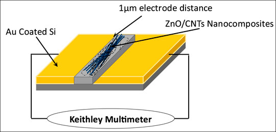
In this work, sensors were prepared by the Doctor Blade method. The glass substrate was washed by the aforementioned process. Electrode formation is shown in Figure 6. The electrodes were formed by RH evaporation of Au on glass substrates. For the study, 95% pure Au of 1.5 µm (1,500 nm) thickness was deposited on substrates at a distance of 10 cm from the source to substrates. A fine diamond cutter was used to separate electrodes at 1 µm distance. Separations of electrodes were confirmed by using a digital multimeter. ZnO nanostructures along with CNTs were scraped away from the growth substrate. The peel was carefully placed on electrode junctions, and 5 µL of 95% pure CH3OH was poured dropwise on the peeled material to stick nanostructures on the respective substrate. The prepared sensors were used to sense UV light by using a Keithley multimeter 2,100 with different timings of UV light exposures.
4 Results and Discussion
4.1 X-Ray Diffraction Analysis
XRD results revealed that the ZnO perfect crystal is a wurtzite structure. A very sharp and prominent peak was observed, as shown in Figure 7, indicating an extensive growth in the (201) plane. Peaks at 66.3o and 67.86o with the planes (200) and 112), respectively, were merged with the peak (201) at 69.01o significant of ZnO, matched with JCPDS No. 01–089-1,397.
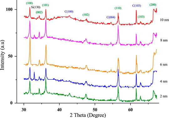
FIGURE 7. XRD pattern of ZnO/CNT nanocomposites over unannealed Au layer with various thicknesses on the Si substrate.
In Figure 7, carbon peaks are observed at 42.8o, 61.1o, and 75.6o with (100), (103), and (110) planes, respectively, according to JCPDS No. 00–002-0,456. It was observed in the presence of pure MWCNTs, as reported earlier in the literature (Bharti, 2020). The MWCNT peaks are showing less intensity as compared to ZnO because they are emended in thick ZnO nanostructures, as reported by Ranjithkumar, R. et al. (Ranjithkumar et al., 2019). These peaks showed a shift of 1o throughout the graph which confirms the ZnO/CNT nanocomposite. The shift is due to the stress caused by ZnO nanostructures which had grown through MWCNTs (Sapkota, 2019). High crystallinity and phase purity were confirmed at 6 and 8 nm layers of Au by sharp peak intensities. ZnO nanostructures at these thicknesses showed a smaller value of full width at half maximum (FWHM) symbolized high defect concentrations. The XRD pattern of unannealed Au on Si substrates showed good crystallinity and phase purity with high defect concentration levels. The slight variation in the intensity of XRD peaks was due to the thickness of the Au layer which caused a change in growth planes, resulting in structural variation. There are some other factors which also affect the intensity of XRD peaks i.e., systematic accuracy, instrumental effects, sample orientation, its placement, phase concentration, crystallite size, and density of ZnO nanostructures on Si substrates.
In Figure 8, sharp peaks of ZnO were observed at (100), (002), (101), (102), (110), and (103) planes whereas peaks at 66.3o, 67.86o, and 69.01o with planes (200), 112), and (201), respectively, were overlapping each other. The XRD pattern is matched with JCPDS No. 01–089-1,397. Carbon peaks were indicated at (100) and (110) as in JCPDS No. 00–002-0,456 [110]) with a shift of 1o due to stress. Growths of the ZnO nanostructure interact with CNTs at a high temperature causing mechanical stress. So it confirms the formation of ZnO and CNT nanocomposites. The substrate peak Si (100) peak at 28.3o was observed at 2- and 10-nm Au thickness samples.
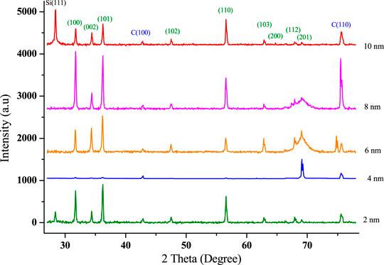
FIGURE 8. XRD pattern of ZnO/CNT nanocomposites over annealed Au layer of various thicknesses on the Si substrate.
The annealed Au layer on the Si substrate showed higher intensities and FWHM than unannealed Au layer samples. The value of FWHM was decreased prominently, as compared to Figure 7, which indicated an increase in defect concentrations. Variation in the peak’s intensity was due to the difference in Au thickness in preannealed Si with the Au layer and change in nanostructures. The Au–Si samples gave unified nucleation points for the ZnO structural growth. Polycrystallinity was developed due to two types of Au–Si substrate alloy droplets and pure Au droplets for condensation of source vapors. Unannealed Au layer samples did not show growth on different planes as there was only Au droplets for condensation of ZnO vapors. This pattern is completely supported by the results of FE-SEM as in the growth of the polar plane which is shown for nanobelts and nanosheets. The XRD graph exhibited a hexagonal wurtzite nanostructure of ZnO. Nanocomposites of ZnO and CNTs were confirmed. The annealed Au layer sample showed poly-crystallinity, higher defect concentrations, and smaller crystallite size, while unannealed Au layer samples showed purity of phase, similarity in growth planes, and relatively larger crystallite size. The prominent peak (201) plane had extended growth in the basal plane for unannealed Au layer on the Si sample.
4.2 Field Emission Scanning Electron Microscopy
4.2.1 Nanobelt Structure
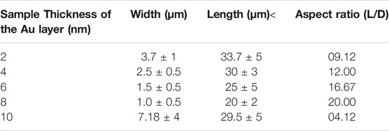
Field emission scanning electron microscopy (FE-SEM) was used to investigate the morphology, grain size, and shape of nanostructures. Synthesis of ZnO/CNT nanocomposites was performed at different thicknesses of the Au layer catalyst on both annealed and unannealed Si substrates. The flow rate of Ar gas, temperature, and other parameters were kept constant throughout the experiment. Thickness of the Au catalyst varied from 2 nm, 4 nm, 6 nm, 8 nm, and 10 nm samples, as shown in Table 1. Multiple structures were obtained on different thicknesses depending upon the nucleation size of the seeds. VLS growth was majorly dependent on the thickness of the catalyst layer. Annealing of Au-coated Si substrates prior to the synthesis had shown a major decrease in the size of structures and uniformity of the structures in samples, as shown in Figures 9A–J.
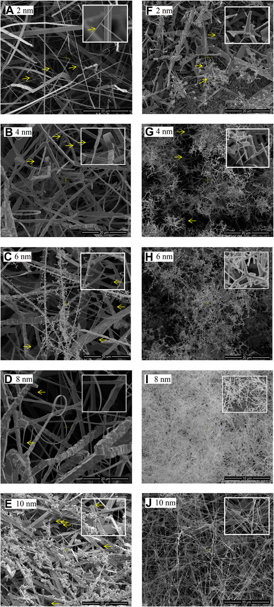
FIGURE 9. FE-SEM images of ZnO/CNT nanocomposites (A) Nanobelts and nanowires (B) Nano belts and nanorods (C) Nanobelts and nanorods (D) Nanobelts and microrods (E) Nanosheets and nanowires (F) Nanobelts, microrods, microcombs, and multipods (G) Multipods (H) Multipods (I) Nanowires (J) Nanowires and initial-staged nanosheets.
Nanobelts were observed in unannealed Au layer thicknesses of 2 nm, 4 nm, 6 nm, and 8 nm samples. The average length and width of nanobelts were decreased with the increase in Au thickness in unannealed Si samples. The rings of nanobelts were observed, as shown in Figure 9A, a unique property of ZnO nanostructures. It was due to the polar surfaces and basal planar growth which enabled the nanobelts to roll in the form of a complete ring (Lao et al., 2003). Morphology of nanostructures was dependent on the thickness of the Au layer. The larger the droplet size, the lesser will be the supersaturation and rate of diffusion. So the nanobelts showed a decrease in size. The aspect ratio increased with the increase in Au thickness, which highly affects the sensing capability of the material. In VLS growth, vapors were evaporated in the molecular form at a high temperature. The stoichiometry of the molecules was also satisfied. While condensing of vapors through Au droplets on the substrate, the stoichiometry of cations and anions were arranged in a pattern that every anion faces a cation. This arrangement stabilized the structure and charges their symmetry around a small nucleus. Every molecule arranged itself around the nucleus. Some parameters are given in Table 1.
At high temperature, mobility of ZnO vapors was quite high that lowered the energy of the surface, which inclined to be flat unlike in nanocombs. To avoid agglomeration of ZnO on the surface, the molecules were arranged in rough growth sites, which turned to be active sites for growth of nanobelts (Wang and Geng, 2005).
4.2.2 Micro and Nanorod Structures
Micro and nanorod structures were observed in unannealed Au layer samples at thicknesses of 4 nm, 6 nm, and 8 nm. There was an increase in the width and decrease in the length of rods with the increase in thickness of the Au layer. These nanorods were formed along the (001) plane (c-axis) as this is the major growth plane. The 6-nm thickness sample indicates a high level of growth in the (001) plane with respect to other planes which is the reason of its higher aspect ratio (Roper et al., 2007). Morphology of the nanostructure was majorly depending on local temperature during synthesis, rate of surface diffusion, and accessibility of ZnO vapors to Au droplets for supersaturation. Because of the lower diffusion rate in large droplets of the thicker Au layer, the nanorods showed a rapid increase in the width of rods. The details are given in Table 2.
4.2.3 Nanosheet Structure
Self-catalyzed growth is reported as the reason for growth of nanosheets. The synthesis of nanosheets was a three-step process. The nanowire was grown by VLS growth which was followed by the teeth growth of 1-D branched from the nanowire; finally, the interspace between the two teeth was filled by 2-D growth. Comb teeth were formed by a slow rate of diffusion and supersaturation of droplets in the source vapor environment. The VS growth was started in an unstable environment. Lack of oxygen concentration in the supersaturation level was increased in the vapor phase. The increase in the Au droplet size, temperature, and oxygen shifted the nanostructure from 1-D to 2D structures (Zhai et al., 2009).
4.2.4 Micro and Nanocomb Structures
Comb-like structures were grown on annealed Au-coated Si substrates in the 2-nm thickness sample. Figure 9F shows microsize combs of ZnO structures. The teeth of combs were grown from one side of the belt; the other side of the belt was smooth. The comb teeth were parallel to each other with triangular tips. Bases of the teeth of combs to the tips were presented clearly in FE-SEM images. The morphological instability of the supersaturated Au droplet was responsible for the side growth of comb teeth. Growth array of nanotips and nanofingers on either sides of the nanobelt was due to the surface polarity of ZnO. ZnO growth was along the (001) plane because of the surface polarity as the growth rate was reasonably high. The origination of teeth from the nanobelt in the comb-like structure was due to the self-catalyzed mechanism (Hierold, 2009).
4.2.5 Multipods and Tetrapod Structure
Multipods were synthesized at different thicknesses of Au layer substrates in annealed samples (2 nm, 4 nm, and 6 nm thickness). In primary thickness of Au, the size was quite large in microranges and reduced up to nanoranges with the increase in Au thickness, whereas the aspect ratio increases with the increase in Au thickness in annealed Au layer samples. Images showed that multipods have nanorods and nanobelts originating from a single nucleation point. The exact reason for synthesis of these structures is still unknown. ZnO tetrapods and multipods are reported in the literature (Lee et al., 2009). The octahedral structure of ZnO offers high effective surface energy in Zn rather than oxygen, so ZnO fine nanorods and nanobelts can be grown from Zn surfaces, resulting in multipods and tetrapods. The wurtzite structure of ZnO has two different atoms Zn and oxygen. Zn is a reactive agent due to the d-shell, whereas oxygen is passive in VLS growth. The difference in nature of two elements forced the ZnO to develop polar surfaces. The higher the supersaturation of droplets, the higher will be the possibility of availability of polar surfaces which were responsible for random growth. The growth rate of the crystal of ZnO was directly reliable on accessibility of ZnO atoms in the catalyst droplet and rate of diffusion at that thickness of the catalyst.
4.2.6 Nanowire Structure
Nanowires were observed on annealed Au-coated Si substrates at the thickness of 8 nm and 10 nm samples, respectively. The decrease in length and width was observed with the increase in Au layer thickness in unannealed samples, whereas the annealed Au layer showed an increase in length and decrease in width with respect to Au thickness. Nanosheets were clearly observed at 10 nm in the annealed Au-coated Si sample. With the increase in dwell time, nanowires may form uniform nanosheets. The aspect ratio decreases in unannealed Au layers, but it shows a dramatic increase in annealed Au layer samples. The annealing of catalyst layers exhibited a considerable change in morphology. At 2-nm thickness of the Au layer sample, a variety of nanostructures were observed, whereas on further increase in thicknesses of the Au layer sample, the multipod nanostructure showed uniformity with the decrease in the structural size up to the nanometer range. After 6-nm thick Au layer sample, the nanostructure showed a structural shift and increase in the length to form nanowires of micron length up to 10-nm thickness of the catalyst layer sample.
4.2.7 CNTs
. In Figure 9, yellow arrows are placed to stop the CNTs. In Figure 9A, ZnO/CNT nanocomposites can clearly be seen inset. ZnO nanowires show the non-uniformity of thickness along the length whereas the CNTs are having a uniform thickness all along the length; the images show coherence with the literature (Ko et al., 2012). In Figures 9B–G, presence of CNTs can be seen in the background as they were deposited by the drop casting method prior to the growth of ZnO nanostructures by the VLS method. In Figures 9H–J, the CNTs’ presence were difficult to spot due the thick growth of ZnO multipods and nanowires.
4.3 Raman Spectroscopy and Photo Luminance
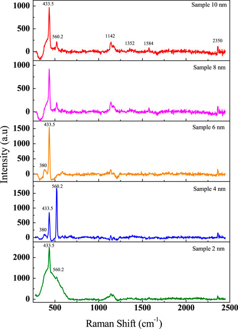
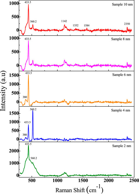
Raman spectroscopy helps to investigate vibrational properties of the samples. In Figures 10,11, Raman graphs for both annealed and unannealed Au layer on Si substrates are shown. A1 + E1 + 2E2, active modes in Raman spectra are allowed by Group theory (Carotta et al., 2009). In the smaller Raman shift region, ZnO peaks at 380-1 and 433.5-1-1 were observed. The ZnO peak at 380 cm-1 was credited as the A1 mode which was due to the transverse optical mode (TO), whereas that of 433.5 cm-1 was attributed to the E2 mode with non-optical phonons of ZnO. 1142-1, 1352-1, and 1584-1-1 peaks were noticed in the higher Raman shift region. 560.2 cm-1 and 1,142 cm-1 peaks were in accordance with the E1 mode which is due to longitudinal optical (LO) and 2LO modes of ZnO (Amin et al., 2014). 1,352-1 and 1584-1-1 peaks are signature peaks of carbon. The peaks at 1,352 cm−1 and 1,584 cm−1 represent D and G modes, respectively; these peaks revealed the presence of CNTs in each sample (HullavaradHullavarad et al., 2009). The 2D mode was also seen in a wider spectrum, whereas the peak at 2,350 cm−1 confirms graphene presence (Amin et al., 2014). The peak at 964 cm−1 is noticed in unannealed Au layer catalyst (Choi et al., 2002). This peak was present in the annealed Au layer sample, but it was not prominent in annealed Au-coated Si due to the increased intensity of ZnO and CNT peaks.
The reason behind broader peaks in both treatments, with respect to pure ZnO nanostructures, was the residual stress of CNTs on n ZnO nanostructures and introduction of oxygen defects (Zhang et al., 2010). The structural deformation in MWCNTs increased in FWHM of peaks and generated D and G bands.
Peaks at 1,352 cm−1 and 1,584 cm−1 of carbon showed evidence of ZnO/CNT nanocomposites. This nanocomposite has higher oxygen vacancies in the ZnO nanostructure, which provide electron to the conduction band in sensing applications. A prominent increase in conductivity was expected during inspection of electrical properties with respect to pure ZnO nanostructure.
Optical band properties of ZnO/CNT nanocomposites were investigated by photo luminance (PL) spectroscopy at room temperature (RT) with He-Cd (325 nm). In Figure 12, the PL spectra of unannealed Au layers on Si substrates are shown in the range of 375–390 nm with intense emission peaks at 379, 380, 381, 383, and 385 nm with energies 3.27, 3.26, 3.25, 3.23, and 3.22 eV, respectively. The peaks showed a red shift with increase in Au thickness. Variation in ZnO nanostructures caused a shift in the near-band edge (NBE) region. In this study, 3.27, 3.26, 3.25, 3.23, and 3.22 eV energy emissions correspond to nanowires, nanorods, microrods, nanobelts, and nanosheets, respectively. The band gap of the ZnO nanostructure is well-known at 382 nm with 3.24 eV. These peaks show an introduction of variety of intrinsic defects during synthesis of nanostructures. The peak at 379 nm was much intense than other peaks in the NBE region. The intensity was due to the presence of nanowires which have a high surface to volume ratio, so relatively more defects were introduced such as oxygen vacancies (Vo), Zn vacancies (VZn), anticite defects (OZn), and interstitial zinc (Zni).
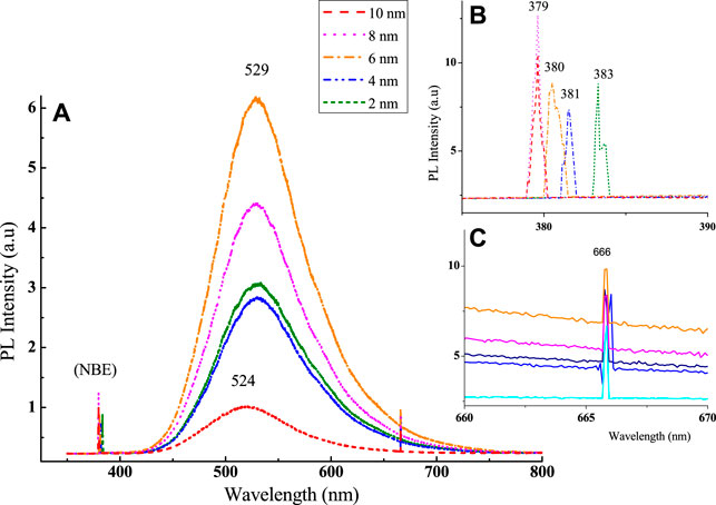
FIGURE 12. (A) PL spectrum of unannealed Au layer of various thicknesses on Si at room temperature (B) PL spectrum in NBE region and (C) shows Si peaks in the lateral region.
The ZnO PL spectra showed peaks at 520 nm in the literature (Djurišić and Leung, 2006), which is observed at 524 nm in the visible region with an energy of 2.36 eV in Figure 12A. This wide and intense peak has a shift of 4 nm due to mechanical interaction of ZnO with CNTs. The lower intensity of the peak at the 6-nm thick Au layer sample indicates a considerable increase in oxygen vacancies and surface recombination effects in ZnO/CNT nanocomposites. Figure 12C showed a new peak with considerable intensity at 649 nm with 1.91 eV which is an attribute of the Si substrate. The intensity of the PL spectrum showed a constant decrease with increase in Au thickness, but at the thickness of 8 nm, it showed a sharp increase. This increase in peak is due to the increase in the band gap with the increase in recombination of the electron hole pair with a rise in energy transfer within neighboring ions. The geometry of samples get in order, so there is a prominent decrease in crystal defects and oxygen vacancies. Low intensity showed good UV sensing as they have higher separation between photo-induced ions with more oxygen vacancies and surface defects.
The PL spectrum of annealed Au layer samples is shown in Figure 13. NBE showed peaks at 379, 380, 381, and 383 nm with their corresponding energies 3.27, 3.26, 3.25, and 3.23 eV. In Figure 13B, unlike in unannealed Au layer samples, peaks exhibited a blue shift with respect to the Au thickness because the ZnO nanostructure comes from nanobelts to nanowires. The commonly reported band gap of the ZnO nanostructure was at 382 nm with 3.24 eV. The smaller the width of ZnO nanostructures, the higher will be the presence of intrinsic defects such as oxygen vacancies (Vo), Zn vacancies (VZn), anticite defects (OZn), and interstitial zinc (Zni). Nanowires showed vividly intense peaks because of high defect concentrations, high surface-to-volume ratio, and high intensity ratio. In Figure 13A, highly intense peaks appeared at 529 nm with energy 2.34 eV for 2, 4, 6, and 8 nm samples, whereas at the 524 nm peak with energy 2.36 eV appeared at 10 nm. Commonly, the ZnO peak appeared at 520 nm (Djurišić and Leung, 2006). There was a shift of 4 nm for 10 nm thickness and 9 nm for other Au thickness samples. CNTs interact mechanically with the ZnO nanostructure which was responsible for the peak shift. Another prominent peak appears at 666 nm with 1.86 eV energy. The intensity variation was different than in unannealed Au layer samples. The spectrum showed a slight decrease in the early increase of Au thickness (2 and 4 nm). Later on, the intensity showed a significant increase at 6 nm thickness; then, it decreased in pattern up to 10 nm thickness. The increase in peak intensity was due to the ordered geometry at 6 nm thickness which increased the band gap and charge recombination. This exhibited lack of structural defects and oxygen vacancies. Annealed Au layer Si samples showed far lower intensities than unannealed Au layer samples. The higher surface defects increased oxygen vacancies, high rate of separation in photo-induced ions, reduced band gap, high separation rate of ions which was supportive for photocatalytic applications, and UV-sensing applications observed in annealed Au layer samples. The peak shift 524–529 nm was an indication of the formation of strong ZnO and CNT interaction and high level of defects due to the Au–Si sample. This resulted in two seeds for condensation of source vapors (alloy and pure Au) for nucleation, which generated a disorder in the crystal structure. Moreover, the Si peak showed a red shift in annealed Au layer samples at 649–666 nm which is due to the presence of the SiO layer deposited during annealing of the substrate with the catalyst layer. This shift exhibited an oxygen-deficient center on the substrate.
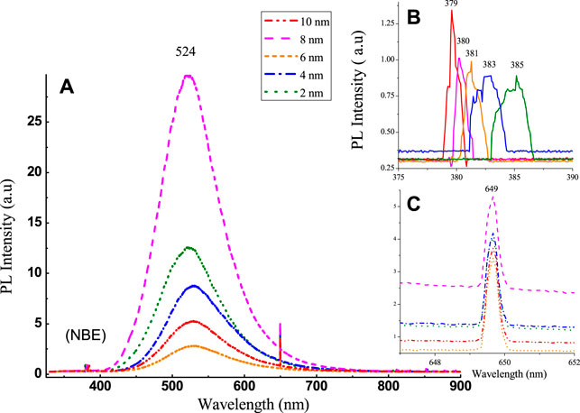
FIGURE 13. (A) PL spectrum of the annealed Au layer of various thicknesses on the Si substrate at room temperature (B) PL spectrum in the NBE region, and (C) shows Si peaks in the lateral region.
4.4 Sensing Applications
Electrons moved from the valence band to conduction band as ZnO/CNT nanocomposites were exposed to UV light of wavelength 315–365 nm (UV Philips Lamp 18 W). The UV light absorbed in samples corresponded to the difference in the band gap of the material, resulting in the flow of current in a circuit and decrease in resistance. As soon as the UV light was switched off, the electrons move back to their energy band, and the material exhibited an instant increase in resistance. In UV-sensing applications, photo conductivity was exploited. The ZnO bandgap energy was in the UV range, which makes it promising for UV-sensing while CNTs are good conductors, which increase conductivity and signal response of sensors. Nanostructures have a high surface-to-volume ratio which makes them highly effective for UV sensing at room temperature.
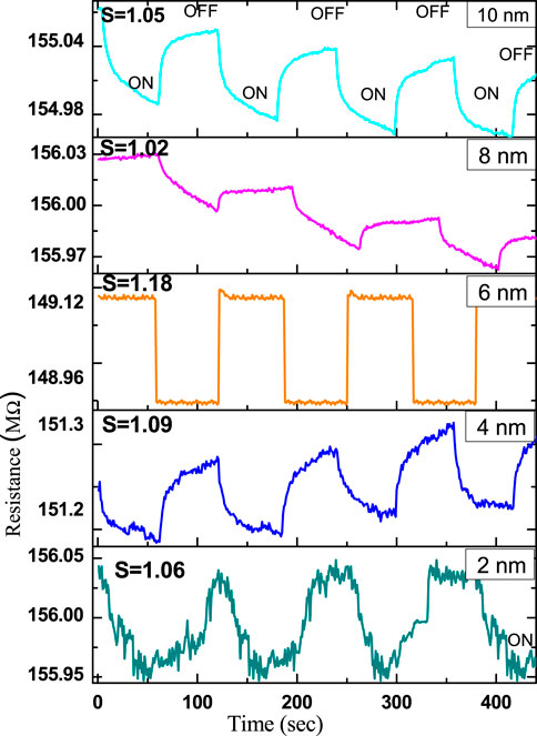
The response of UV sensing in 1-min cycle of unannealed Au layers on the Si substrate and ZnO/CNTs nanocomposite resistance vs. time are shown in Figure 14. UV sensors at 6 nm of the thickness sample showed an instant response and recovery on exposure to UV light along high signal response (S = Rd/Rl where S is signal response, Rd is the resistance in dark and Rl is the resistance in UV light) i.e., 1.18 with respect to other Au thickness samples. FE-SEM images clearly showed the presence of branched nanorods with the increase of surface-to-volume ratio and defect concentration which was responsible for effective sensing. PL results also predicted the 6-nm thickness sample as good sensing nanocomposites. Samples with thickness of 4 and 10 nm respond far as compared to recovery time with the signal response 1.09 and 1.05, respectively. The value of resistance was not reached to the initial value in the 1-min cycle for 10 nm thickness. It was due to the presence of conduction electrons in the conduction band after switching off UV light, whereas for the 4-nm Au thickness sample, behavior was inverse because of multipods, nanorods (S = 1.96), and nanobelts (S = 1.45), which offered roughness in sensor surface response and thickness variation over the sensor and allowed resistance to increase in each cycle. The sample with 2-nm Au thickness showed no uniformity in graph but have a higher signal response, and the response with the 8-nm thickness sample was (S = 1.06).
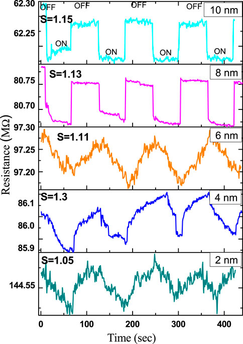
In Figure 15, UV-sensing showed good results at 8 and 10 nm thickness with quick response and recovery time and signal response being 1.13 and 1.15, respectively. The uniformity of nanostructures assured the same resistance level in all other samples. Nanowires had good crystallinity and high surface defect ratios which made them perfect for sensing. Interaction of CNTs and ZnO nanowires was also strong. Multipod structure was generated at 4- and 6-nm Au thickness samples. These structures showed poor response and recovery in UV-sensing with the signal response 1.30 and 1.11, respectively. In 4 nm of Au thickness, the sample has nanobelts, nanorods, and nanosheets generating from the same nucleation point. This lack of uniformity of the ZnO nanostructure affects the sensing results. However, the sample at 6 nm Au thickness generated multipods with nanorods only; UV-sensing showed relatively better results than the sample with 2 nm thickness. Annealed Au layer samples showed good sensing results at higher thicknesses of 8 and 10 nm Au layers, whereas un-annealed Au layer samples exhibited better results at 6 nm thickness with higher signal response (1.18) than 8 nm (1.13) and 10 nm (1.15) of annealed Au-coated Si samples. Good sensing is an attribute of high crystallinity, smaller crystallite size, higher defect concentrations, higher oxygen vacancies, and ZnO/CNT nanocomposites.
As the smaller crystallite sizes have a high surface ratio, higher oxygen vacancies allowed ZnO to attract higher oxygen molecules in the absence of UV light and developed a strong negative charge space which was the basic cause to photoconductivity of ZnO nanostructures. UV-sensing responsivety, response time and decay time of Un-annealed and annealed Au layer at various thicknesses are given in Table 3.

TABLE 3. UV-sensing responsivity, response time, and decay time of unannealed and annealed Au layers at various thicknesses.
Conclusion
Different morphologies were synthesized at different Au-coated thicknesses on Si substrates by the VLS method successfully. The wurtzite structure of ZnO and high crystallinity was confirmed by XRD results with sharp ZnO peaks. The carbon peaks showed a constant shift in the XRD pattern in annealed and unannealed Au-coated layer samples which confirm the presence of ZnO/CNT nanocomposites. ZnO nanostructures exhibited an increase in lateral growth of the nanostructure with the increase in Au thickness up to 8 nm. The direct relation between the length and Au thickness was showing a dramatic change after 8 nm of Au thickness. The inversion in relation between the width of the ZnO nanostructure and Au thickness nanostructures was seen in FE-SEM in the annealed Au-coated substrate, whereas annealed Au coating retained the direct relation between the length and Au thickness at 10 nm. ZnO nanostructures with a higher aspect ratio showed good results in UV-sensing. Similar peaks were observed in both set of samples in Raman spectroscopy. Broader peaks in unannealed Au layer samples indicate the inhomogeneous crystalline size with the same crystal orientation. Raman peaks at 1,353 cm−1 and 1,584 cm−1 were an evidence of ZnO/CNT nanocomposites. The peak shift of 4 nm was observed in major peaks which confirm ZnO/CNT nanocomposites. The Si peak showed shift in annealed Au layers due to the oxidation of Si substrates during annealing with the Au layer. Significant results were observed on 6-nm Au thickness due to the branched structures in unannealed samples. Annealed Au-coated samples showed quick response and efficient UV-sensing with ZnO nanowires at 8 and 10-nm Au thickness samples.
Data Availability Statement
The original contributions presented in the study are included in the article/Supplementary Material; further inquiries can be directed to the corresponding author.
Author Contributions
This work was done in Thin Films Technology Research Laboratory department of Physics, COMSATS University (CUI) Islamabad, Pakistan. NS is an in charge of the laboratory. MB and MA are PhD students. Whereas NA and SJ are PhD students. All the authors have contributed in this manuscript.
Conflict of Interest
The authors declare that the research was conducted in the absence of any commercial or financial relationships that could be construed as a potential conflict of interest.
Publisher’s Note
All claims expressed in this article are solely those of the authors and do not necessarily represent those of their affiliated organizations, or those of the publisher, the editors, and the reviewers. Any product that may be evaluated in this article, or claim that may be made by its manufacturer, is not guaranteed or endorsed by the publisher.
Acknowledgments
Higher education commission Pakistan is acknowledged for financial support through a project No. 9294/NRPU/R&D/HEC/2017. The authors would also be thankful to CU Islamabad for necessary funds for the project. Authors would like to thank Dr. Masoom Fatima and Dr. Waqar Adil Syed of IIU Islamabad for valuable discussion during this research work.
References
Afrin, R., Shah, N. A., Abbas, M., Amin, M., and Bhatti, A. S. (2013). Design and Analysis of Functional Multiwalled Carbon Nanotubes for Infrared Sensors. Sensors Actuators A: Phys. 203, 142–148. doi:10.1016/j.sna.2013.08.018
Ahmed Jamal, G. R., Islam, M. R., Rahman, M. A., Meem, J. F., and Sathie, R. A. (2017).Chirality Dependence of Gas Adsorption Property of Single wall Carbon Nanotubes Msf, 889, 248–252. doi:10.4028/www.scientific.net/msf.889.248
Albiss, B. A., Sakhaneh, W. A., Jumah, I., and Obaidat, I. M. (2010). ${\Hbox{NO}}_{2}$ Gas Sensing Properties of ZnO/Single-Wall Carbon Nanotube Composites. IEEE Sensors J. 10 (12), 1807–1812. doi:10.1109/jsen.2010.2049739
Ali, G. M., and Chakrabarti, P. (2010). ZnO-based Interdigitated MSM and MISIM Ultraviolet Photodetectors. J. Phys. D: Appl. Phys. 43, 415103. doi:10.1088/0022-3727/43/41/415103
Amin, M. (2015). Development of Highly Sensitive UV Sensor Using Morphology Tuned ZnOnanostructures. Appl. Phys. A 118, 595. doi:10.1007/s00339-014-8764-x
Amin, M., Manzoor, U., Islam, M., Bhatti, A., and Shah, N. (2012). Synthesis of ZnO Nanostructures for Low Temperature CO and UV Sensing. Sensors 12, 13842–13851. doi:10.3390/s121013842
Amin, M., Shah, N. A., Bhatti, A. S., and Malik, M. A. (2014). Effects of Mg Doping on Optical and CO Gas Sensing Properties of Sensitive ZnO Nanobelts. CrystEngComm 16, 6080–6088. doi:10.1039/c4ce00153b
Bai, S., Wu, W., Qin, Y., Cui, N., Bayerl, D. J., and Wang, X. (2011). High-Performance Integrated ZnO Nanowire UV Sensors on Rigid and Flexible Substrates. Adv. Funct. Mater. 21, 4464–4469. doi:10.1002/adfm.201101319
Bharti, V. (2020). Fabrication of Magnetic Cobalt Ferrite Nanocomposites: an Advanced Method of Removal of Toxic Dichromate Ions from Electroplating Wastewater. Korean J. Chem. Eng. 37, 1157. doi:10.1007/s11814-020-0516-3
Carotta, M. C., Cervi, A., di Natale, V., Gherardi, S., Giberti, A., Guidi, V., et al. (2009). ZnO Gas Sensors: a Comparison between Nanoparticles and Nanotetrapods-Based Thick Films. Sensors Actuators B: Chem. 137, 164–169. doi:10.1016/j.snb.2008.11.007
Chen, X., Wong, C. K. Y., Yuan, C. A., and Zhang, G. (2013). Nanowire-based Gas Sensors. Sensors Actuators B: Chem. 177, 178–195. doi:10.1016/j.snb.2012.10.134
Choi, K.-S., Lichtenegger, H. C., Stucky, G. D., and McFarland, E. W. (2002). Electrochemical Synthesis of Nanostructured ZnO Films Utilizing Self-Assembly of Surfactant Molecules at Solid−Liquid Interfaces. J. Am. Chem. Soc. 124, 12402–12403. doi:10.1021/ja0275562
Comini, E. (2009). Quasi-one Dimensional Metal Oxide Semiconductors: Preparation, Characterization and Application as Chemical Sensors. Prog. Mater. Sci. 54, 1. doi:10.1016/j.pmatsci.2008.06.003
Djurišić, A. B., and Leung, Y. H. (2006). Optical Properties of ZnO Nanostructures. small 2, 944. doi:10.1002/smll.200600134
Farbod, M., Joula, M. H., and Vaezi, M. (2016). Promoting Effect of Adding Carbon Nanotubes on Sensing Characteristics of ZnO Hollow Sphere-Based Gas Sensors to Detect Volatile Organic Compounds. Mater. Chem. Phys. 176, 12–23. doi:10.1016/j.matchemphys.2016.03.004
Fu, H.-C., Wang, W.-C., Wu, W.-W., and Yeh, P.-H. (2012). Ultrahigh Sensitivity ZnO Nanosensor with Schottky Nanojunction. Meet. Abstr. MA2012-01, 1643. doi:10.1149/ma2012-01/45/1643
Givargizov, E. I. (1975). Fundamental Aspects of VLS Growth. J. Cryst. Growth 31, 20–30. doi:10.1016/0022-0248(75)90105-0
Hernández, S. C. (2012). Hybrid ZnO/SWNT Nanostructures Based Gas Sensor. Electroanalysis 24 (7), 1613. doi:10.1002/elan.201200135
Johansson, J., Wacaser, B. A., Dick, K. A., and Seifert, W. (2006). "Growth Related Aspects of Epitaxial Nanowires," Nanotechnology, 17, S355. doi:10.1088/0957-4484/17/11/s21
Khanderi, J., Hoffmann, R. C., Gurlo, A., and Schneider, J. J. (2009). Synthesis and Sensoric Response of ZnO Decorated Carbon Nanotubes. J. Mater. Chem. 19 (28), 5039–5046. doi:10.1039/b904822g
Kim, H., and Sigmund, W. (2002). Zinc Oxide Nanowires on Carbon Nanotubes. Appl. Phys. Lett. 81, 2085–2087. doi:10.1063/1.1504877
Kim, S. (2009). Enhanced Ultraviolet Emission from Hybrid Structures of Single-Walled Carbon nanotubes/ZnO Films. Appl. Phys. Lett. 94, 3113. doi:10.1063/1.3148646
Ko, Y. H., Kim, M. S., and Yu, J. S. (2012). Structural and Optical Properties of ZnO Nanorods by Electrochemical Growth Using Multi-Walled Carbon Nanotube-Composed Seed Layers. Nanoscale Res. Lett. 71, 13–16. doi:10.1186/1556-276X-7-13
Lao, J. Y., Huang, J. Y., Wang, D. Z., and Ren, Z. F. (2003). ZnO Nanobridges and Nanonails. Nano Lett. 3, 235–238. doi:10.1021/nl025884u
Lee, J. M., Pyun, Y. B., Yi, J., Choung, J. W., and Park, W. I. (2009). ZnO Nanorod−Graphene Hybrid Architectures for Multifunctional Conductors. J. Phys. Chem. C 113, 19134–19138. doi:10.1021/jp9078713
Li, S. Y., Lee, C. Y., and Tseng, T. Y. (2003). Copper-catalyzed ZnO Nanowires on Silicon (100) Grown by Vapor-Liquid-Solid Process. J. Cryst. Growth 247, 357–362. doi:10.1016/s0022-0248(02)01918-8
Li, X. L., Li, C., Zhang, Y., Chu, D. P., Milne, W. I., and Fan, H. J. (2010). Atomic Layer Deposition of ZnO on Multi-Walled Carbon Nanotubes and its Use for Synthesis of CNT-ZnO Heterostructures. Nanoscale Res. Lett. 5, 1836–1840. doi:10.1007/s11671-010-9721-z
Nasser, A. (2020). A New Method for Preparing ZnO/CNT Nanocomposites with Enhanced Photocatalytic Degradation of Malachite green under Visible Light. J. Photochem. Photobiol. A: Chem. 389, 112207. doi:10.1016/j.jphotochem.2019.112207
Ranjithkumar, R., Arasi, S. E., Sudhahar, S., Nallamuthu, N., Devendran, P., Lakshmanan, P., et al. (2019). Enhanced Electrochemical Studies of ZnO/CNT Nanocomposite for Supercapacitor Devices. Physica B: Condensed Matter 568, 51–59. doi:10.1016/j.physb.2019.05.025
Roper, S. M., Davis, S. H., Norris, S. A., Golovin, A. A., Voorhees, P. W., and Weiss, M. (2007). Steady Growth of Nanowires via the Vapor-Liquid-Solid Method. J. Appl. Phys. 102, 034304. doi:10.1063/1.2761836
Sadananda Kumar, N., Bangera, K. V., and Shivakumar, G. K. (2014). Effect of Annealing on the Properties of Zinc Oxide Nanofiber Thin Films Grown by spray Pyrolysis Technique. Appl. Nanosci 4, 209–216. doi:10.1007/s13204-012-0190-9
Sapkota, K. P. (2019). Solar-light-driven Efficient ZnO–Single-Walled Carbon Nanotube Photocatalyst for the Degradation of a Persistent Water Pollutant Organic Dye. Catalysts 96–498. doi:10.3390/catal9060498
Hullavarad, S., Hullavarad, N., Look, D., and Claflin, B. (2009). "Persistent Photoconductivity Studies in Nanostructured ZnO UV Sensors," Nanoscale Res. Lett. 4. 1421. doi:10.1007/s11671-009-9414-7
Sinha, N., Ma, J., and Yeow, J. T. W. (2006). Carbon Nanotube-Based Sensors. j nanosci nanotechnol 6, 573–590. doi:10.1166/jnn.2006.121
Subodh, B. (2017b). ZnO-CNT Nanocomposite Based Gas Sensors—An Overview. Sensor Lett. 15 (12), 955. doi:10.1166/sl.2017.3912
Subodh, B. (2017a). ZnO-CNT Nanocomposite: a Device as Electrochemical Sensor. Mater. Today Proc. 4 (4), 5552. doi:10.1016/j.matpr.2017.06.012
Tiwari, J. N., Tiwari, R. N., and Kim, K. S. (2012). Zero-dimensional, One-Dimensional, Two-Dimensional and Three-Dimensional Nanostructured Materials for Advanced Electrochemical Energy Devices. Prog. Mater. Sci. 57, 724–803. doi:10.1016/j.pmatsci.2011.08.003
Vyas, R., Sharma, S., Gupta, P., Prasad, A. K., Tyagi, A. K., Sachdev, K., et al. (2012). “CNT-ZnO Nanocomposite Thin Films: O2 and NO2 Sensing. Advanced Materials Research 585, 235–239. doi:10.4028/www.scientific.net/amr.585.235
Wan, Q., Li, Q. H., Chen, Y. J., Wang, T. H., He, X. L., Li, J. P., et al. (2004). Fabrication and Ethanol Sensing Characteristics of ZnO Nanowire Gas Sensors. Appl. Phys. Lett. 84, 3654–3656. doi:10.1063/1.1738932
Wang, N., Cai, Y., and Zhang, R. Q. (2008). Growth of Nanowires. Mater. Sci. Eng. R: Rep. 60, 1–51. doi:10.1016/j.mser.2008.01.001
Wang, Z. L., and Geng, M. (2005). “Nanotechnology and Nanomanufacturing,” in SemiconductorManufacturing Handbook, 57.
Wang, Z. L. (2003). “Nanodevice, Nanosensors and Nanocantilevers Based on Semiconducting Oxide Nanobelts,” in Nanowires and Nanobelts (Springer), 3–19. doi:10.1007/978-0-387-28747-8_1
Wang, Z. L. (2009). ZnO Nanowire and Nanobelt Platform for Nanotechnology. Mater. Sci. Eng. R: Rep. 64, 33–71. doi:10.1016/j.mser.2009.02.001
Wen, H.-C., Hung, C.-I., Tsai, H.-J., Lu, C.-K., Lai, Y.-C., and Hsu, W.-K. (2012). ZnO-coated Carbon Nanotubes: an Enhanced and Red-Shifted Emission Band at UV-VIS Wavelength. J. Mater. Chem. 22, 13747–13750. doi:10.1039/c2jm31487h
Wong, M. (2003). Electrochemical Growth of ZnO Nano-Rods on Polycrystalline Zn Foil. Nanotechnology 14, 968
Xia, Y., Yang, P., Sun, Y., Wu, Y., Mayers, B., Gates, B., et al. (2003). One-dimensional Nanostructures: Synthesis, Characterization, and Applications. Adv. Mater. 15, 353–389. doi:10.1002/adma.200390087
Xu, C. (2005). Growth of Ga-doped ZnO Nanowires by Two-step Vapor Phase Method. Appl. Phys. Lett. 86, 133107
Yin, H., Wang, Q., Geburt, S., Milz, S., Ruttens, B., Degutis, G., et al. (2013). Controlled Synthesis of Ultrathin ZnO Nanowires Using Micellar Gold Nanoparticles as Catalyst Templates. Nanoscale 5, 7046–7053. doi:10.1039/c3nr01938a
Zhai, T., Fang, X., Liao, M., Xu, X., Zeng, H., Yoshio, B., et al. (2009). A Comprehensive Review of One-Dimensional Metal-Oxide Nanostructure Photodetectors. Sensors 9, 6504–6529. doi:10.3390/s90806504
Zhang, H., Du, N., Chen, B., Li, D., and Yang, D. (2009). Carbon Nanotube-ZnO Nanosphere Heterostructures: Low-Temperature Chemical Reaction Synthesis, Photoluminescence, and Their Application for Room Temperature NH3 Gas Sensor. Sci. Adv. Mat 1 (1), 13–17. doi:10.1166/sam.2009.1002
Zhang, W.-D., Xu, B., and Jiang, L.-C. (2010). Functional Hybrid Materials Based on Carbon Nanotubes and Metal Oxides. J. Mater. Chem. 20, 6383–6391. doi:10.1039/b926341a
Keywords: UV sensors, nanotubes, metal oxide, semiconductors, microstructures
Citation: Basit M, Abbas M, Ahmad N, Javed S and Shah NA (2022) Synthesis of ZnO/CNT Nanocomposites for Ultraviolet Sensors. Front. Mater. 9:835521. doi: 10.3389/fmats.2022.835521
Received: 14 December 2021; Accepted: 28 January 2022;
Published: 15 March 2022.
Edited by:
Josep Albero, Spanish National Research Council (CSIC), SpainReviewed by:
Mahendra Dashrath Shirsat, Dr. Babasaheb Ambedkar Marathwada University, IndiaRaid Ismail, University of Technology, Iraq
Copyright © 2022 Basit, Abbas, Ahmad, Javed and Shah. This is an open-access article distributed under the terms of the Creative Commons Attribution License (CC BY). The use, distribution or reproduction in other forums is permitted, provided the original author(s) and the copyright owner(s) are credited and that the original publication in this journal is cited, in accordance with accepted academic practice. No use, distribution or reproduction is permitted which does not comply with these terms.
*Correspondence: Nazar Abbas Shah, bmFiYmFzcXVyZXNoaUB5YWhvby5jb20=
 Maryam Basit1
 Nazar Abbas Shah