 Vikas Kashyap1*
 Hariom Pawar
 Kapil Saxena
95% of researchers rate our articles as excellent or good
Learn more about the work of our research integrity team to safeguard the quality of each article we publish.
Find out more
ORIGINAL RESEARCH article
Front. Mater. , 24 November 2022
Sec. Colloidal Materials and Interfaces
Volume 9 - 2022 | https://doi.org/10.3389/fmats.2022.1022317
In the present study, the controllable fabrication of silicon nanowires (Si NWs) with vertical alignment was accomplished using metal assisted chemical etching (MACE). The different characteristics, such as structural, morphological, chemical, optical, and dielectric properties were analyzed using X-ray diffraction (XRD), field emission scanning electron microscope (FESEM), Raman spectroscopy, ultraviolet-visible diffuse reflectance spectroscopy (UV-DRS), and LCR [inductance (L), capacitance (C), and resistance (R)] meter (volume of the gas-sensing chamber is 650 mm3). It was revealed from the morphological study i.e., from the FESEM that p-type Si NWs are smaller in size than n-type Si NWs which is attributable to the energy band gap. The optical band gap (Eg) is observed to increase from 1.64 to 1.89 eV with the decreasing of the crystallite size and the optical reflection spectra of the Si NWs show a shift toward a lower wavelength (blue shift). Moreover, Raman spectra verified the red-shifted, asymmetrically broadened Raman line-shapes, which provides information about the size confinement effect in Si NWs. The MACE approach is excellent for synthesizing nanowire structures for use in gas-sensing applications due to its flexibility. The sensitivity of synthesized Si NWs was tested for NO2 gas. The sensor method is unique based on the testing of the device in the presence of a test gas because the use of the gas-sensing setup has the potential to measure the change in resistance by varying frequency, temperature, and time.
The field of electronics and photonics has seen semiconductor nanowires (NWs) emerge as a promising candidate in recent years due to their wide range of possible applications (Xi et al., 2007; Gonchar et al., 2016; Li and Kwok, 2018; Gonchar et al., 2019). Silicon (Si) is gaining importance as a promising approach for an industrial revolution in semiconductor technology due to its technological-based properties.
The enormous growth of microelectronics has benefited Si process technology. Si is potentially the only material that satisfies all of the requirements, including its non-toxicity, strong absorption optics, and high performance (greater than 10%). The manufacturing of effective devices to fuel our economies has shifted toward the more stable Si nano-crystals and NWs. Various methods are available for the synthesis of Si NWs with vast numbers of applications. Si nanostructures (NSs) have been manufactured using a wide range of processes, including chemical etching, epitaxial growth, and electron beam lithography (Hasan et al., 2013; Puglisi et al., 2019). The simplest and lowest cost method for creating NSs is metal-assisted chemical etching (MACE) (Li et al., 2013). Si NWs have enormous potential for usage in thermoelectric power, lithium-ion batteries, sensors, and solar energy conversion (Peng et al., 2008; Kim et al., 2010; Liang et al., 2014; Toor et al., 2016; Ghosh et al., 2018; Singh et al., 2018; Kashyap et al., 2021a).
The goal for the scientific community has been to improve human health and the environment by monitoring unsafe and poisonous substances, gases, micro-organisms, and radiation. One-dimensional (1D) material-based sensors are extremely efficient and compatible with recent manufacturing techniques resulting in data that are useful for health and environmental monitoring (Zhu and Zeng, 2017). Nanostructures such as nanowires can be the path to effective and advantageous sensor materials. The scientific community is working to develop sensors that can provide alerts of potential risks in response to a number of pressing issues, including protecting human health, the environment, and safety. Additionally, Si NWs may simply be scaled up for use in gas-sensing applications employing the room temperature MACE approach. The usage of gas-sensing technology is widespread in both household and industrial settings. The most crucial characteristics of gas-sensor devices are their sensitivity, working temperature, selectivity, energy consumption and cost of production (Zhu and Zeng, 2017; Mirzaei et al., 2018; Bhati et al., 2020).
According to the type of material, the depletion layer either forms or deforms during the gas-sensing phenomenon which includes the transfer of electrons between the sensing material and the target gases. Zhang et al. (2016) conducted the first study in the field of Si NW based gas sensors.
Si NWs for gas sensing have a sensing function that is fairly comparable to a conventional semiconductor gas sensor, since a single Si NW unit has high sensitivity in a nanosensor applications. Peng et al. (2009) created two independent gold electrodes that have a limit of detection (LOD) of 500 ppb against NO2 and are placed on the top of a vertical Si NW array. To increase the sensitivity of the Si NW array for gas detection, each one should be connected to an electrical circuit (Zhang et al., 2016; Morganti et al., 2021). The problem has been solved by developing a number of methods for fabricating a continuous electrode on top of a Si NW array.
This research focuses on functionalization of Si NWs, synthesis, and the application of Si NWs as gas sensors. In this study, we have fabricated Si NWs using the MACE method and the role of quantum confinement has been established. Techniques such as ultraviolet-visible diffuse reflectance spectroscopy (UV-DRS) was used for the band-gap variation in the nano regime for the different doped Si NWs, and the noble method of gas sensing was introduced to detect NO2 gas at lower concentrations.
In this study, the MACE technique was used to fabricate Si NWs samples of n-type Si (100) (doped with ∼103 phosphorous atoms/cm3) and p-type Si (100) (doped with ∼103 Boron atoms/cm3) having resistivity 1–10 Ω cm, thickness 265 ± 25 μm, 2 × 2 cm2, keeping all other parameters constant. For the deposition process, hydrofluoric acid (HF) (Sigma-Aldrich, assay 99.9%) and silver nitrate (AgNO3) (Sigma-Aldrich, assay 99.9%) were taken in the proportion of 4.8 M and 5 mM, respectively, for 60 seconds at room temperature to deposit silver nanoparticles (Ag NPs). The etching solution was made by taking HF and hydrogen peroxide (H2O2) (Merck, assay 99.9%) in the proportion of 4.6 and 0.5 M, respectively. After the deposition process, the samples were etched for a duration of 40 min each. The etched wafers were then transferred to HNO3 to dissolve the remaining Ag NPs and they were then dipped into HF solution to remove the oxide layer (Supporting Information). The samples are named as n40 (n-type and etching duration of 40 min) and p40 (p-type and etching duration of 40 min).
For characterizing the samples, X-ray diffraction (XRD) was recorded by using Cu (Kα) radiation (0.154 nm). Morphological analysis of Si NWs was carried out using a field emission scanning electron microscope (FESEM) (HITACHI SU8010). The Raman spectra were recorded using a HORIBA Jobin Youn iHR-550 spectrometer equipped with a cooled charge-coupled device (CCD) detector. An excitation line with a wavelength of 785.0 nm was produced using an air-cooled Ar+ ion laser and the samples were exposed for 10 seconds. The laser power density was less than 107 mW/cm2. The dielectric and sensing properties were investigated using a LCR [inductance (L), capacitance (C), and resistance (R)] meter (HIOKI, IM3536) and a gas-sensing system, respectively.
The XRD patterns of the Si NWs for the n-type and p-type samples are shown in Figure 1. The XRD peak for the n40 sample is observed at 2θ = 69.16°, assigned (004) plane, and for the p40 sample is observed at 2θ = 68.8°, lattice plane (004). The sharp and narrow peak observed in the n40-type indicates improvements in crystallinity (Westra et al., 2010; Ghahramanifard et al., 2018).
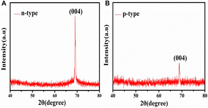
FIGURE 1. XRD of Si NWs (A) n40 and (B) p40.
The average crystalline size of Si NWs was calculated by the Scherrer equation (Minin and Minin, 1994):
where D is the crystalline size (average), θ is the diffraction angle, λ is the wavelength (0.154 nm) of radiation used for the diffraction, and β is the full-width at half maximum (FWHM) of the observed peaks (∼0.002 for both samples). The estimated crystalline size of the Si NWs is 89 nm and 73 nm for the n40 and p40 samples, respectively.
The XRD peak broadening occurs as a result of a deviation from the ideal crystal. This broadening can be primarily caused by the solution, crystallite size, and micro strain; the micro strain is a major factor among these and estimated as (Samy et al., 2019)
where
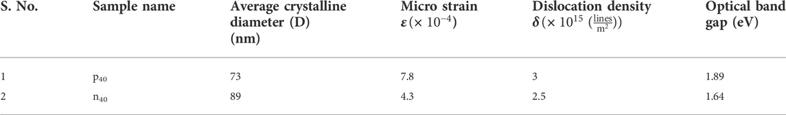
TABLE 1. Summarized microstructural and elastic parameters of the Si NWs.
Dislocation is a topological defect; it is the length of dislocation lines in a unit volume (dislocation density) of a crystalline material, i.e., defects present in the samples, mathematically expressed as (Ravichandran and Philominathan, 2009)
where δ = dislocation density, k = dimensionless shape factor (its value is 0.89), and θ and D are the same as above. The small values of δ obtained in the current investigation support the good crystallinity of the fabricated sample i.e., Si NWs, by using the MACE method. It was found that the dislocation density and micro strain decrease with an increase in crystallite size showing lower imperfections as shown in Table 1. This might be because Si NWs have larger crystallites due to a shift in the dopant (n-type or p-type) which results in a decrease in the occurrence of grain boundaries (Joshi et al., 2003; Begum et al., 2012).
Scanning electron micrographs of Si NWs are depicted in Figure 2. Figures 2A–D depict magnified 45o-tilt and cross-sectional FESEM images of Si NWs on n (Figures A,B) and p (Figures C,D) Si (100) wafers (1–10 Ω cm), keeping other parameters constant, such as chemical concentration and etching time (i.e., 40 min). The length of the Si NWs is calculated using ImageJ software; it is approximately 10 μm and 11 µm for n40 and p40 Si NWs, respectively, as shown in Figure 3.
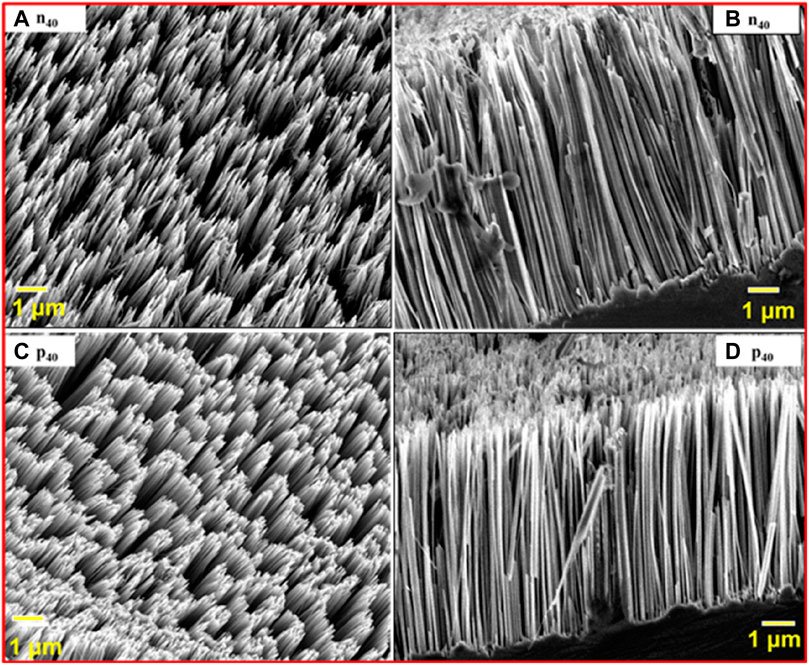
FIGURE 2. 45o-tilt view and cross-sectional FESEM images of samples (A,B) for the n40 Si NW (C,D) and p40 Si NW, respectively.
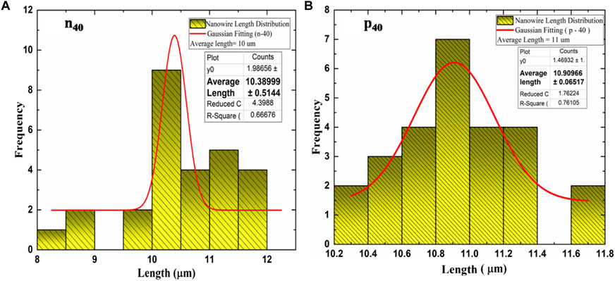
FIGURE 3. Average length of the Si NWs (A) n40 and (B) p40 using ImageJ software.
Figures 2A–D reveal that, as we deal with different doping (n40 and p40), the length of deposited Si NWs increases due to sufficient oxidizing species present in the solution to oxidize the Si (Peng et al., 2011). The p40 sample has a denser structure and has a greater length compared to the n40 sample, as shown in Figure 3.
The average size (diameter) estimated using ImageJ software, of the Si NWs in n40 and p40 are 97 nm and 80 nm, as shown in Figures 4A,B, respectively. According to previous studies the variation in the shape of Si NWs is due to the occurrence of inhomogeneous nucleation of Ag on the Si (100) wafer (Hutagalung et al., 2017; Naffeti et al., 2020; Rouis et al., 2021). We conclude that the lower size of the p40-type Si NW compared to the n40-type Si NW is attributable to the energy band gap because as the size reduces the band gap increases. As discussed earlier, the p-type has a band gap of 1.89 eV, while the n-type has a band gap of 1.64 eV (Rouis et al., 2021). Figure 4 depicts the average diameter of n-type and p-type Si NWs, which we calculated using ImageJ software by selecting the Si NWs from the FESEM images. By selecting the diameter of all images of the Si NWs, we take the average length, which comes out as 80 nm and 97 nm for n-type and p-type Si NWs, respectively.
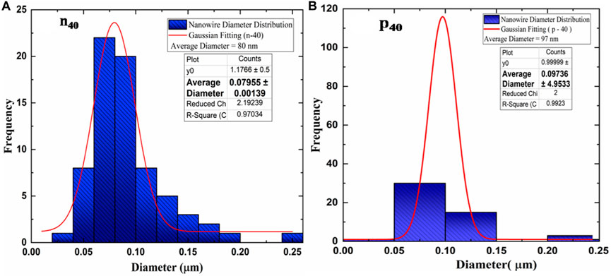
FIGURE 4. Average diameter of the Si NWs (A) n40 and (B) p40 using ImageJ software.
The total reflectance of Si NWs onto n40 Si (100) and p40 Si (100) in the wavelength range of 250 nm–850 nm is shown in Figures 5A,B. It is observed that the p-type Si NW has better light-trapping than the n-type Si NW. In the n40 sample, the observed reflectance was ∼9% in the UV region (<300 nm), ∼6% in the visible region (300–700 nm), and about 3.5% in the IR region (>700 nm), which is less than the percentage of reflectance given by crystalline Si (c-Si) (reflectance = 66%). In the p40 sample, the observed reflectance was ∼3% in the UV region (<300 nm), ∼4% in the visible region (300 nm–700 nm), and about 3% in the IR region (>700 nm). Moreover, the total reflectance depends upon on the length of the Si NWs; this corresponds to the reflection, which becomes lower with longer lengths of Si NWs. Total reflectance decreased for the p40 sample because the charge carrier gradually increases on the textured surface (Kashyap et al., 2022).
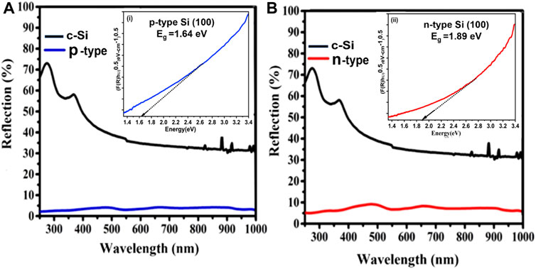
FIGURE 5. Total reflection of the Si NWs (A) p-type and (B) n-type with an inset of the optical band gap (i) for n40 and (ii) for p40.
The Kubelka–Munk function was used to transform reflection into absorption spectra (Chiu and Li, 2009; Yogi et al., 2017; Kashyap et al., 2021b):
where s denotes the scattering coefficient. If s → 0 (no scattering occurs), all the light will be either transmitted or absorbed, while if k → 0 (no absorption or transmission occur), all the light will be reflected.
The optical band gap can be estimated by (Shukla and Dixit, 2016; Venkatesan et al., 2019)
where F(R) is the Kubelka–Munk function, which is equivalent to the optical absorption coefficient, Eg is the optical band gap of the Si NW, A is a constant, and n is the power factor which is impacted by several electronic transitions. The plot between (F(R) hν)1/2 vs. photon energy (Eg) for the n40 type- and p40-type Si NWs is depicted in the inset of Figures 5A,B, given by (i) and (ii), respectively. The estimated values are 1.64 and 1.89 eV for the n40- and p40-typetype samples, respectively. It is observed that the n40 sample has a lesser band gap in comparison to the p40 sample because the conductivity of the n40 sample is higher.
This might be explained by a growth in crystallite size and a reduction in imperfections. The plot between (F(R) hν)1/2 vs. photon energy (Eg) for n40-type and p40-types in the inset of Figure 5 [i.e., (i) and (ii)] illustrates that the Si NWs are linear throughout a large range of photon energy. This suggests that the synthesized Si NWs have a direct optical band gap. The optical band gap of these materials can be calculated by extrapolating the linear portion of the curve to the energy axis. It is noticed that the resulting band gap falls from 1.89 eV (for the p40-type) to 1.64 eV (for the n40-type). According to the usual relationship between band gap and crystallite size, the band gap rises as the crystallite size decreases (summarized in Table 1). Due to the size confinement in the Si NWs, the observed values of Eg are greater than the value of the bulk Si (1.12 eV) (Gao et al., 2007). The variation of different parameters with crystalline size is also confirmed in Figure 6.
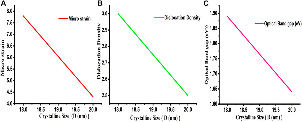
FIGURE 6. Variation of different parameters with crystalline size. (A) Micro strain (B) Dislocation Density (C) Optical Band gap.
The Raman spectra for the n40 and p40 samples are given in Figure 7, along with a comparison with bare Si. A Raman peak at 520 cm−1 with a FWHM of 3.5 cm−1 of c-Si was found due to the Raman active zone center symmetry point
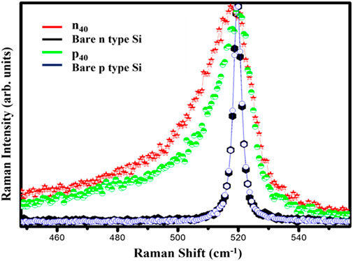
FIGURE 7. Raman analysis for the n40 and p40 samples with their bare counterpart.
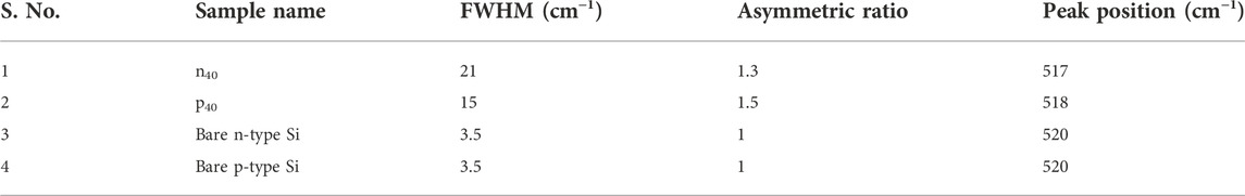
TABLE 2. Calculations of various parameters from the Raman analysis.
Figure 7 shows that in comparison to their bulk equivalent, the Raman spectra for Si NWs are red-shifted and asymmetrically widened. An asymmetric broadening of the Raman line-shape is caused by the combination of the Fano effect and phonon confinement (Kumar, 2013; Yogi et al., 2016; Saxena et al., 2017; Bhujel et al., 2018). Analysis of the Raman line-shape characteristics such as peak position, peak asymmetry, and FWHM which also reveals the presence of phonon confinement in both samples. The wavenumber was observed at 517.4 ± 0.26, and 518.4 ± 0.18 cm−1 for the n40 and p40 samples respectively, with varying asymmetry ratios due to the quantum confinement (QC) effect. This range of wavenumbers of the line is generally defined with a long-range Raman scattering line.
The asymmetry arises due to the presence of nano-scale size confinement (Li et al., 2005; Kumar, 2013). Phonon confinement in Si NWs is thought to be the cause of the red-shifted, asymmetrically widened Raman line-shapes, as shown in Figure 7. The Raman line-shapes are wider on the lower energy side of the peak for n40 semiconductors (asymmetry ratio 1.3), but wider on the higher energy side of the peak for p40 semiconductors (asymmetry ratio 1.5), as there is more electron–phonon confinement in the n40 sample.
In vertically aligned Si NW arrays, metal electrodes must be linked to the ends of the Si NWs. Copper wire was used for the connecting wires and silver epoxy was used to join the wires after they had been tested and chosen for ohmic contact formation. The Si nanowire tips must be in complete contact with a metal electrode; otherwise, a short circuit would result. Figure 8 is a representation of the ohmic contact made with the fabricated samples of Si NWs.
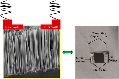
FIGURE 8. Ohmic contacts with Si NWs and electrodes.
The change of electrons in the presence of the electric field is responsible for the change in the capacitance of the Si NWs. The dielectric properties of the Si NWs were investigated in the form of a thin film of dimensions 2 mm
where
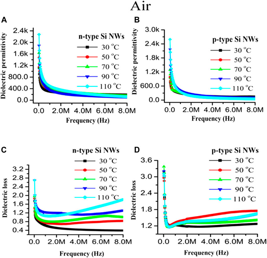
FIGURE 9. Dielectric permittivity and dielectric loss with varying temperature of (A,C) n40 Si NWs and (B,D) p40 Si NWs as a function of frequency, respectively.
The dielectric loss showed a very low loss of energy in operation with varying frequency and time for both devices, which indicates that the devices will show enhanced sensing phenomenon for the detection of NO2 gas. The dielectric loss as a function of frequency with variation of temperature is depicted in Figures 9C,D. The dielectric loss decreased rapidly as the frequency initially increased until 1 MHz and 0.5 MHz for n-type and p-type Si NWs, respectively, and became constant but as the temperature increased from 30
The AC conductivity as a function of frequency with varying temperature is depicted in Figure 10. It is clearly observed from Figures 9A,B that as the frequency increased from 100 Hz to 8 MHz and the AC conductivity also increased in linear order and became highest at 8 MHz for both types of sensing materials. The AC conductivity of the n40 Si NW increased with increasing temperature from 30°C to 110°C and became highest at 110°C, while this was found to be lower for the p40 Si NW. The change in conductivity with increasing temperature is observed due to the hopping conduction mechanism (Saidi et al., 2017).
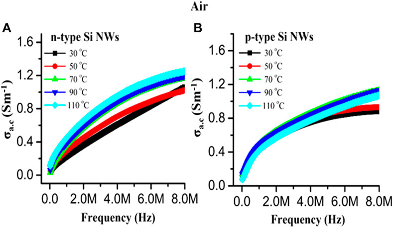
FIGURE 10. The AC conductivity with varying temperatures for (A) n40 Si NWs and (B) p40 Si NWs as a function of frequency.
The instrument used for the gas-sensing analysis is shown in Figure 11, which comprised a LCR meter furnace followed by a gas-sensing arrangement.
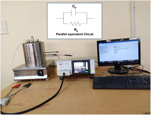
FIGURE 11. Schematic of a dielectric setup including an equivalent circuit, a furnace, a gas-sensing system, and a LCR meter (parallel equivalent circuit is shown in the inset).
The sensing mechanism behind the response toward oxidizing gas (NO2) is based on the change in resistance or conductance of the semiconductor devices in the presence of air and an oxidizing gas environment. The change in resistance as a function of frequency at 30

FIGURE 12. Electrical resistance as a function of frequency at 30
The ratio of change in resistance matter for the identification of gas response was calculated using Eqs 7, 8. The objective of the present study is to investigate the change of resistance at 30°C with varying concentrations of NO2 gas for the fabrication of room-temperature detection devices.
Figures 11B,D show the change in resistance as a function of frequency with varying temperatures of the sensor devices in the presence of oxidizing gas. The change in resistance or conductance also depends on the n-type or p-type behavior of the devices. Usually, the resistance of n40 type Si NWs in the presence of oxidizing gas such as NO2 increases with increasing the concentration of the target gas (10 ppm–250 ppm) while decreasing for p40-type Si NWs owing to the dual modulation of space charge constituency between the adsorbed oxygen with the sensing element and NO2 gas atmospheres. This occurs because of the physically powerful electron-withdrawing capabilities of NO2; the accumulation of a hole in p40-type Si NW based sensors occurs due to the withdrawing of electrons, which increases the conductivity of the sensor (Cao et al., 2013) with increasing concentrations, while decreasing for n40-type Si NW based sensors.
The gas-sensing behavior of the sensors was investigated by observing the change in resistance in air and oxidizing gas atmosphere using the following relationship (Pawar et al., 2020):
where R (%) is the sensitivity of the target gas,
The gas-sensing response as the function of frequency with varying gas concentrations from 10 ppm to 250 ppm is shown in Figures 13A,B. The sensing response of the n40-type Si NW based sensor showed that the response toward NO2 gas initially decreased with increasing frequency, reaching a minimum at a certain frequency and then increasing again at higher frequencies. The concentration of the oxidizing gas introduced in the gas-sensing unit, varying from 10 ppm to 250 ppm, exhibited an excellent gas response at lower concentrations, which is at 50 ppm, and a minimum response at higher concentrations at all frequency ranges because the fabricated sensor had a small dimension suitable to detect gas precisely at lower concentrations, but at higher concentrations, the adsorbed layer of the O−2 and gas-interacting surface was saturated; hence, the free electrons were not available in the sensor element, which can propagate current through the device, and as a result the resistance increased rapidly, which reduced the gas response of the sensor, while decreasing in the case of the p40-type Si NW sensor. In the presence of NO2 gas, as the frequency increased, the resistance of the sensing device decreased due to saturation polarization which improved the gas sensitivity. A chemiresistive sensor’s sensitivity is a resistance-dependent mechanism as the maximum change in resistance was observed in the presence of NO2 gas, while in the air atmosphere, the gas response increased.
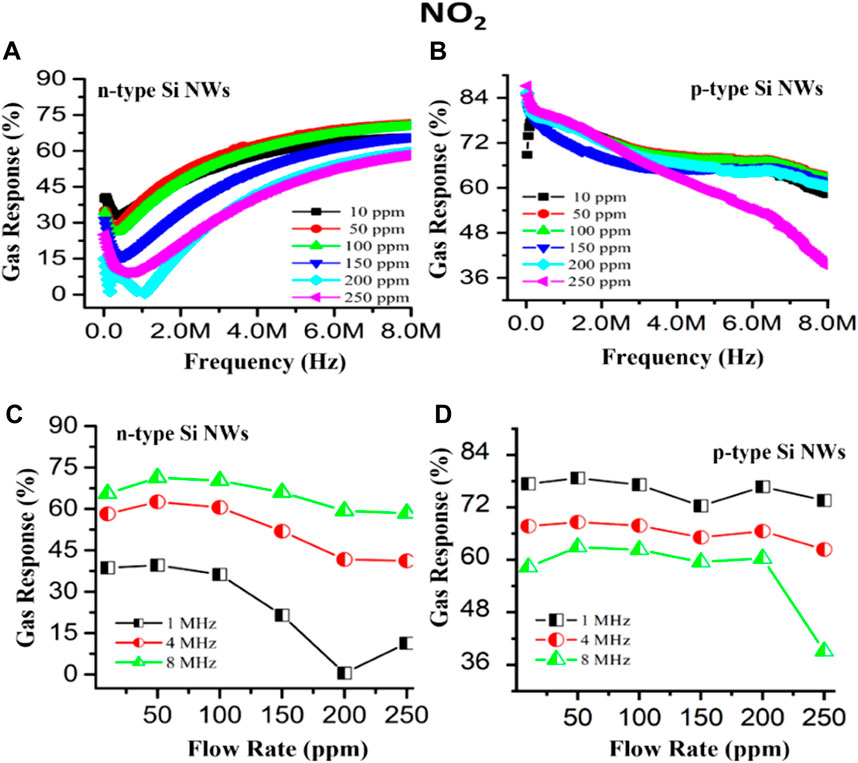
FIGURE 13. Gas-sensing response as a function of frequency with varying concentrations for (A) the n40 Si NW and (B) the p40 Si NW and at fixed frequencies with varying NO2 gas concentrations for (C) the n40 Si NW and (D) the p40 Si NW at room temperature, respectively.
The gas response R (%) of n40-type and p40-type Si NW sensors as a function of concentrations at specific frequencies of 1, 4, and 8 MHz is depicted in Figures 13C,D.
Figure 13C shows the gas response of the n40-type Si NW based gas sensor, with the maximum sensing performance at 50 ppm found to be 35%, 63%, and 68% at 1, 4, and 8 MHz, respectively, while this was 75%, 68%, and 62% for the p40-type Si NW based sensor, as illustrated in Figure 10D. The aforementioned results revealed that the p40-type Si NW based sensor is the best for the detection of NO2 gas at room temperature and at lower frequencies, while the n40-type Si NW-based sensor is the best for the detection of NO2 gas at room temperature and higher frequencies.
The low-cost MACE method was utilized for synthesizing Si NWs. The structural analysis of the synthesized Si NWs confirmed that as the crystallite size increased, the dislocation density decreased simultaneously. The morphological analysis showed that the array of Si NWs had a length of approximately 10 ± 0.5 and 11 ± 0.06 µm and an approximate average size (diameter) of 97 ± 5 nm and 80 ± 0.001 nm for the n40 and p40 samples, respectively. The band gap of the synthesized Si NWs was observed to decrease from 1.89 eV (for the p-type) to 1.64 eV (for the n-type) which is a remarkable outcome for gas-sensing applications. Due to greater electron–phonon confinement in the n40 sample, the Raman line-shape was wider on the lower energy side of the peak for the n40-type semiconductor (asymmetry ratio: 1.3) but was wider on the higher energy side of the peak for the p40-type semiconductor (asymmetry ratio: 1.5). The dielectric study confirmed the lower dielectric values of the synthesized Si NWs at room temperature, which is a strong indication for the sensing performance of the fabricated device. Regarding the gas-sensing response of the n40-type Si NW based gas sensor, the maximum sensing performance at 50 ppm was found to be 35%, 63%, and 68% at 1, 4, and 8 MHz, respectively, while this was 75%, 68%, and 62% for the p40-type Si NW based sensor, which confirms that the p40-type Si NW based sensor is the best for the detection of NO2 gas at room temperature and lower frequencies, while the n40-type Si NW-based sensor is the best for the detection of NO2 gas at room temperature and higher frequencies.
The raw data supporting the conclusions of this article will be made available by the authors, without undue reservation.
VK: conceptualization, methodology, writing—review and editing, validation, resources, and data curation. HP: writing—review and editing, validation, resources, and data curation. CK: formal analysis and visualization. NC: supervision. KS: supervision and investigation.
We would like to thank to Dr. Deepshikha Rathore (ASAS, Amity University, Jaipur, Rajasthan, India) for the use of the dielectric and gas-sensing facilities. we also acknowledge financial support via Senior Research Fellowship (SRF) from the University Grants Commission (UGC), India. The author acknowledges the Sophisticated Analytical Instrumentation Facility (SAIF) and Prof. G. S. S. Saini (Department of Physics, Panjab University, Chandigarh, India) for using and recording the Raman spectroscopy facility.
The authors declare that the research was conducted in the absence of any commercial or financial relationships that could be construed as a potential conflict of interest.
All claims expressed in this article are solely those of the authors and do not necessarily represent those of their affiliated organizations, or those of the publisher, the editors, and the reviewers. Any product that may be evaluated in this article, or claim that may be made by its manufacturer, is not guaranteed or endorsed by the publisher.
The Supplementary Material for this article can be found online at: https://www.frontiersin.org/articles/10.3389/fmats.2022.1022317/full#supplementary-material
Begum, A., Hussain, A., and Rahman, A. (2012). Effect of deposition temperature on the structural and optical properties of chemically prepared nanocrystalline lead selenide thin films. Beilstein J. Nanotechnol. 3, 438–443. doi:10.3762/bjnano.3.50
Bhati, V. S., Hojamberdiev, M., and Kumar, M. (2020). Enhanced sensing performance of ZnO nanostructures-based gas sensors: A review. Energy Rep. 6, 46–62. doi:10.1016/j.egyr.2019.08.070
Bhujel, R., Rizal, U., Agarwal, A., Swain, B. S., and Swain, B. P. (2018). Synthesis and characterization of silicon nanowires by electroless etching. J. Mat. Eng. Perform. 27, 2655–2660. doi:10.1007/s11665-018-3179-z
Cao, A., Sudhölter, E. J. R., and de Smet, L. C. P. M. (2013). Silicon nanowire-based devices for gas-phase sensing. Sensors Switz. 14, 245–271. doi:10.3390/s140100245
Chiu, S. C., and Li, Y. Y. (2009). SiC nanowires in large quantities: Synthesis, band gap characterization, and photoluminescence properties. J. Cryst. Growth 311, 1036–1041. doi:10.1016/j.jcrysgro.2008.11.099
Gao, S., Liu, D., Xu, D., Li, D., Hong, Y., Chen, H., et al. (2007). Synthesis of Se nanospheres and PbSe nanoshells in solution under refluxing and stirring. Smart Mat. Struct. 16, 2350–2353. doi:10.1088/0964-1726/16/6/039
Ghahramanifard, F., Rouhollahi, A., and Fazlolahzadeh, O. (2018). Electrodeposition of Cu-doped p-type ZnO nanorods; effect of Cu doping on structural, optical and photoelectrocatalytic property of ZnO nanostructure. Superlattices Microstruct. 114, 1–14. doi:10.1016/j.spmi.2017.07.019
Ghosh, S., Dey, S., Das, B., Das, N. S., Sarkar, S., and Chattopadhyay, K. K. (2018). Wettability of metal assisted chemically etched (MaCE) grass like silicon nanowires. Proc. Int. Conf. 2018, 213–217. doi:10.1109/EDKCON.2018.8770405
Gonchar, K. A., Kitaeva, V. Y., Zharik, G. A., Eliseev, A. A., and Osminkina, L. A. (2019). Structural and optical properties of silicon nanowire arrays fabricated by metal assisted chemical etching with ammonium fluoride. Front. Chem. 7, 653–657. doi:10.3389/fchem.2018.00653
Gonchar, K. A., Zubairova, A. A., Schleusener, A., Osminkina, L. A., and Sivakov, V. (2016). Optical properties of silicon nanowires fabricated by environment-friendly chemistry. Nanoscale Res. Lett. 11, 357. doi:10.1186/s11671-016-1568-5
Hasan, M., Huq, M. F., and Mahmood, Z. H. (2013). A review on electronic and optical properties of silicon nanowire and its different growth techniques. Springerplus 2, 151. doi:10.1186/2193-1801-2-151
Hutagalung, S. D., Fadhali, M. M., Areshi, R. A., and Tan, F. D. (2017). Optical and electrical characteristics of silicon nanowires prepared by electroless etching. Nanoscale Res. Lett. 12, 425. doi:10.1186/s11671-017-2197-3
Joshi, R. K., Kanjilal, A., and Sehgal, H. K. (2003). Size dependence of optical properties in solution-grown Pb1 xFexS nanoparticle films. Nanotechnology 14, 809–812. doi:10.1088/0957-4484/14/7/320
Kashyap, V., Chaudhary, N., Goyal, N., and Saxena, K. (2021). Fabrication and characterization of silicon nanowires with MACE method to influence the optical properties. Mater. Today Proc. 49, 3409–3413. doi:10.1016/j.matpr.2021.02.814
Kashyap, V., Kumar, C., Chaudhary, N., Goyal, N., and Saxena, K. (2021). Comparative study of quantum confinements effect present in Silicon Nanowires using absorption and Raman spectroscopy. Opt. Mat. (Amst). 121, 111538. doi:10.1016/j.optmat.2021.111538
Kashyap, V., Kumar, C., Kumar, V., Chaudhary, N., and Saxena, K. (2022). The effect of dopant on light trapping characteristics in random silicon nanowires for solar cell applications. Phys. B Condens. Matter 638, 413953. doi:10.1016/j.physb.2022.413953
Khan, M., Pawar, H., Kumari, M., Patra, C., Patel, G., Dwivedi, U. K., et al. (2020). Effect of concentration of SiC on physicochemical properties of CoFe2O4/SiC nanocomposites. J. Alloys Compd. 840, 155596. doi:10.1016/j.jallcom.2020.155596
Kim, H., Seo, M., Park, M. H., and Cho, J. (2010). A critical size of silicon nano-anodes for lithium rechargeable batteries. Angew. Chem. Int. Ed. 49, 2146–2149. doi:10.1002/anie.200906287
Kumar, R. (2013). Asymmetry to symmetry transition of Fano line-shape: Analytical description. Indian J. Phys. 87, 49–52. doi:10.1007/s12648-012-0183-2
Li, C., Fang, G., Sheng, S., Chen, Z., Wang, J., Ma, S., et al. (2005). Raman spectroscopy and field electron emission properties of aligned silicon nanowire arrays. Phys. E Low-dimensional Syst. Nanostructures 30, 169–173. doi:10.1016/j.physe.2005.08.005
Li, G., and Kwok, H. S. (2018). Silicon nanowire solar cells. Adv. Silicon Sol. Cells 4, 269–298. doi:10.1007/978-3-319-69703-1_10
Li, L., Yao, Y., Lin, Z., Liu, Y., and Wong, C. P. (2013). Low-cost micrometer-scale silicon vias (SVs) fabrication by metal-assisted chemical etching (MaCE) and carbon nanotubes (CNTs) filling. Proc. - Electron. Components Technol. Conf., 581–585. doi:10.1109/ECTC.2013.6575632
Liang, B., Liu, Y., and Xu, Y. (2014). Silicon-based materials as high capacity anodes for next generation lithium ion batteries. J. Power Sources 267, 469–490. doi:10.1016/j.jpowsour.2014.05.096
Minin, I. V., and Minin, O. V. (1994). Elements of diffraction quasi-optics. USA: bridge12 technologies.
Mirzaei, A., Kang, S. Y., Choi, S. W., Kwon, Y. J., Choi, M. S., Bang, J. H., et al. (2018). Fabrication and gas sensing properties of vertically aligned Si nanowires. Appl. Surf. Sci. 427, 215–226. doi:10.1016/j.apsusc.2017.08.182
Morganti, D., Leonardi, A. A., Lo Faro, M. J., Leonardi, G., Salvato, G., Fazio, B., et al. (2021). Ultrathin silicon nanowires for optical and electrical nitrogen dioxide detection. Nanomaterials 11, 1767–1780. doi:10.3390/nano11071767
Naffeti, M., Postigo, P. A., Chtourou, R., and Zaïbi, M. A. (2020). Elucidating the effect of etching time key-parameter toward optically and electrically-active silicon nanowires. Nanomaterials 10, 404. doi:10.3390/nano10030404
Pawar, H., Khan, M., Kumari, M., Tara, U. K. D., Ranveer, P., Kumar, R., et al. (2021). Role of calcination on dielectric properties of BaTiO 3 nanoparticles as a gas sensor. Appl. Phys. A 127, 384. doi:10.1007/s00339-021-04517-6
Pawar, H., Khan, M., Mitharwal, C., Dwivedi, U. K., Mitra, S., and Rathore, D. (2020). Co1−xBaxFe2O4 (x = 0, 0.25, 0.5, 0.75 and 1) nanoferrites as gas sensor towards NO2 and NH3 gases. RSC Adv. 3, 35265–35272. doi:10.1039/d0ra04303f
Peng, C., Gao, J., Wang, S., Zhang, X., Zhang, X., and Sun, X. (2011). Stability of hydrogen-terminated surfaces of silicon nanowires in aqueous solutions. J. Phys. Chem. C 115, 3866–3871. doi:10.1021/jp109963z
Peng, K., Jie, J., Zhang, W., and Lee, S. T. (2008). Silicon nanowires for rechargeable lithium-ion battery anodes. Appl. Phys. Lett. 93, 033105–33114. doi:10.1063/1.2929373
Peng, K. Q., Wang, X., and Lee, S. T. (2009). Gas sensing properties of single crystalline porous silicon nanowires. Appl. Phys. Lett. 95, 243112–243196. doi:10.1063/1.3275794
Puglisi, R. A., Bongiorno, C., Caccamo, S., Fazio, E., Mannino, G., Neri, F., et al. (2019). Chemical vapor deposition growth of silicon nanowires with diameter smaller than 5 nm. ACS Omega 4, 17967–17971. doi:10.1021/acsomega.9b01488
Rasool, K., Rafiq, M. A., Li, C. B., Krali, E., Durrani, Z. A. K., and Hasan, M. M. (2012). Enhanced electrical and dielectric properties of polymer covered silicon nanowire arrays. Appl. Phys. Lett. 101, 023114–023115. doi:10.1063/1.4735278
Ravichandran, K., and Philominathan, P. (2009). Comparative study on structural and optical properties of CdS films fabricated by three different low-cost techniques. Appl. Surf. Sci. 255, 5736–5741. doi:10.1016/j.apsusc.2008.12.076
Rouis, A., Hizem, N., Hassen, M., Amri, C., and Kalboussi, A. (2021). Structural and optical characteristics of silicon nanowires prepared by the Ag-assisted chemical etching method. Bull. Mat. Sci. 44, 94. doi:10.1007/s12034-021-02394-6
Saidi, H., Walid, A., Bouazizi, A., Herrero, B. R., and Saidi, F. (2017). Effects of silicon nanowires (SiNWs) contents on the optical and dielectric properties of poly(3-hexylthiophene):SiNWs nanocomposites. J. Phys. Chem. Solids 107, 1–6. doi:10.1016/j.jpcs.2017.03.011
Samy, K., Ramachandran, K., and Vasantha*, V. (2019). Photocatalytic performances and antibacterial activities of nano-ZnO derived by cetrimide-based Co-precipitation method by varying solvents. Int. J. Innov. Technol. Explor. Eng. 9, 930–938. doi:10.35940/ijitee.b7145.129219
Saxena, S. K., Yogi, P., Mishra, S., Rai, H. M., Mishra, V., Warshi, M. K., et al. (2017). Amplification or cancellation of Fano resonance and quantum confinement induced asymmetries in Raman line-shapes. Phys. Chem. Chem. Phys. 19, 31788–31795. doi:10.1039/c7cp04836j
Shukla, A. K., and Dixit, S. (2016). Raman study of phase transformation from diamond structure to wurtzite structure in the silicon nanowires. J. Phys. D. Appl. Phys. 49, 285304. doi:10.1088/0022-3727/49/28/285304
Singh, N., Sahoo, M. K., and Kale, P. G. (2018). Effect of MACE parameters on length of porous silicon nanowires (PSiNWs). J. Cryst. Growth 496, 10–14. doi:10.1016/j.jcrysgro.2018.05.019
Toor, F., Miller, J. B., Davidson, L. M., Nichols, L., Duan, W., Jura, M. P., et al. (2016). Nanostructured silicon via metal assisted catalyzed etch (MACE): Chemistry fundamentals and pattern engineering. Nanotechnology 27, 412003–412012. doi:10.1088/0957-4484/27/41/412003
Venkatesan, R., Mayandi, J., Pearce, J. M., and Venkatachalapathy, V. (2019). Influence of metal assisted chemical etching time period on mesoporous structure in as-cut upgraded metallurgical grade silicon for solar cell application. J. Mat. Sci. Mat. Electron. 30, 8676–8685. doi:10.1007/s10854-019-01191-6
Westra, J. M., Vavrun̂ková, V., Ŝutta, P., Swaaij, R. A. C. M. M., and Zeman, M. (2010). Formation of thin-film crystalline silicon on glass observed by in-situ XRD. Energy Procedia 2, 235–241. doi:10.1016/j.egypro.2010.07.034
Xi, J. Q., Schubert, M. F., Kim, J. K., Schubert, E. F., Chen, M., Lin, S. Y., et al. (2007). Optical thin-film materials with low refractive index for broadband elimination of Fresnel reflection. Nat. Photonics 1, 176–179. doi:10.1038/nphoton.2007.26
Yogi, P., Mishra, S., Saxena, S. K., Kumar, V., and Kumar, R. (2016). Fano scattering: Manifestation of acoustic phonons at the nanoscale. J. Phys. Chem. Lett. 7, 5291–5296. doi:10.1021/acs.jpclett.6b02090
Yogi, P., Poonia, D., Mishra, S., Saxena, S. K., Roy, S., Kumar, V., et al. (2017). Spectral anomaly in Raman scattering from p-type silicon nanowires. J. Phys. Chem. C 121, 5372–5378. doi:10.1021/acs.jpcc.6b12811
Zhang, A., Zheng, G., and Lieber, C. (2016). Nanowires : Building blocks for nanoscience and nanotechnology. Germany: Springer.
Keywords: FESEM, Raman spectroscopy, dielectric properties, gas sensing, UV-DRS
Citation: Kashyap V, Pawar H, Kumar C, Chaudhary N and Saxena K (2022) Analysis of synthesized doped vertical silicon nanowire arrays for effective sensing of nitrogen dioxide: As gas sensors. Front. Mater. 9:1022317. doi: 10.3389/fmats.2022.1022317
Received: 18 August 2022; Accepted: 02 November 2022;
Published: 24 November 2022.
Edited by:
Alfonso Policicchio, Università della Calabria, ItalyReviewed by:
Maria Josè Lo Faro, University of Catania, ItalyCopyright © 2022 Kashyap, Pawar, Kumar, Chaudhary and Saxena. This is an open-access article distributed under the terms of the Creative Commons Attribution License (CC BY). The use, distribution or reproduction in other forums is permitted, provided the original author(s) and the copyright owner(s) are credited and that the original publication in this journal is cited, in accordance with accepted academic practice. No use, distribution or reproduction is permitted which does not comply with these terms.
*Correspondence: Vikas Kashyap, dmlrYXNrYXNoeWFwNzg2NDdAZ21haWwuY29t; Kapil Saxena, a2FwaWwuc2F4ZW5hQGtuaXQuYWMuaW4=
Disclaimer: All claims expressed in this article are solely those of the authors and do not necessarily represent those of their affiliated organizations, or those of the publisher, the editors and the reviewers. Any product that may be evaluated in this article or claim that may be made by its manufacturer is not guaranteed or endorsed by the publisher.
Research integrity at Frontiers
Learn more about the work of our research integrity team to safeguard the quality of each article we publish.