 Bin Liu1,2
 Pinghui Wu
 Li Lv
Li Lv- 1Rural Revitalization Institute, Linyi University, Linyi, China
- 2Center for International Education, Philippine Christian University, Manila, Philippines
- 3Fujian Provincial Key Laboratory for Advanced Micro-Nano Photonics Technology and Devices, Quanzhou Normal University, Quanzhou, China
- 4School of Physics and Electronic Engineering, Linyi University, Linyi, China
In recent years, solar energy has received extensive attention as a clean and renewable energy. We present a perfect broadband solar absorber based on tungsten and semiconductor GaAs in this paper. The structure of GaAs grating-GaAs film-W substrate has been proposed. And the finite time domain difference method (FDTD) has been used for the numerical simulation of the model. Broadband absorption has been realized in the 500–1,850 nm, by adjusting the parameters of geometry to excite high-efficiency surface plasmon resonance. The absorption spectrum of the structure can be changed by adjusting the geometric parameters to meet different needs. The proposed absorber has incidence insensitive (0–60°) and high short-circuit current characteristics. The structure is simple and easy to manufacture, and has superior photoelectric properties to be application in photothermal conversion, collection and utilization of solar energy.
Introduction
Solar energy is inexhaustible, reliable and less polluting, which is why it is considered the most potential energy (Zhao et al., 2020). As a green energy, solar energy is widely used in many fields (Xiong et al., 2013; Yang et al., 2014; Zhang et al., 2014; Li et al., 2016; Xiao et al., 2017; Li et al., 2018; Tang et al., 2018; Chen P. et al., 2019; Cheng et al., 2022). These advantages have always made how to collect and use solar energy a hot and important issue. The actual solar radiation in the range of about 295–2,500 nm, the design can be perfectly matched to the wavelength band of the solar device is a key to efficient use of solar energy.
GRAPHICAL ABSTRACT. A perfect broadband solar absorber based on tungsten and grating-GaAs was proposed. Broadband absorption has been realized in the 500–1,850 nm. The proposed absorber has incidence insensitive (0–60°). The proposed absorber has high short-circuit current characteristics.
In recent years, solar absorbers have attracted more and more attention as an important energy collect device (Kimpton et al., 2020; Yi et al., 2020; Yu et al., 2020; Li et al., 2021a; Zhou et al., 2021). For an ideal absorber must have a high efficiency of light absorption and many other physical properties, such as polarization stability and adjustability etc. (Jiang et al., 2021a; Li et al., 2021b; Li R. et al., 2021c; Li-Ying et al., 2021; Wu et al., 2021). However, the existing absorbers are generally limited by low temperature tolerance, low light absorption efficiency and materials (Briggs et al., 2010; Li et al., 2020a; Chen et al., 2021a; Chen et al., 2021b; Jiang et al., 2021b). Therefore, a new broadband solar absorber needs to be proposed to solve these problems.
Broadband absorber is an old concept that was proposed many years ago. Over the years, it has been widely used in the fields of solar heating devices, solar cells and photothermal converters (Sobhani et al., 2013; Xiao et al., 2019; Li et al., 2020b; Wang et al., 2021; Zhao et al., 2021). The improvement of broadband absorbers has three main directions. Firstly, it is important to find the most suitable material. Because of the obvious shortcomings of traditional metal materials such as gold and silver, such as high cost and poor heat resistance, people began to pay attention to materials with high melting points such as TiN, tungsten and other, which are different from the original broadband absorber. They not only have a high melting point, but also can be used as effective plasmon excitation materials. Secondly, the nanostructure design of the broadband absorber is also very critical. The multi-layer-metal-insulator (MMI) structure is first used, and then turned to a simpler MIM or IMI nanostructures. Finally, the working range of the broadband absorber was investigated and continuously improved, especially in the ultraviolet to near infrared range. In order to obtain an ideal broadband absorber in practical applications, it is necessary that the proposed absorber can fulfill the requirements mentioned above. For example, Lei et al. (2016) modulated the duty cycle of metal gratings. They simulated the optical characteristics of metal-insulator-metal grating nanostructures and obtained four absorption regions with absorption near 100%. Qin et al. (2020) proposed a solar absorber based on TiN and Ti. The simulation results demonstrate that broadband absorption can be achieved. Jiang et al. proposed a broadband solar absorber based on hyperbolic multilayer metamaterial (HMM) is obtained in greater than 90% absorption from 300 to 2,215 nm (Khavasi, 2015). Although the characteristics of these absorbers are sufficiently superior, their complex nanostructures and various preparations of complex materials make the proposed absorbers imperfect, and it is difficult to apply them in subsequent practical manufacturing. Accordingly, an absorber with structure simpler but also excellent high absorption is presented urgently.
Over here, we proposed a GaAs grating solar absorber which obtain bandwidth with absorption over 90% reaches 1,350 nm. The overall structure only uses two kinds of materials: metal W and semiconductor GaAs, the melting points of them are high and their thermal stabilities are great. Compared with traditional noble metals, W has higher metal loss and is easier to achieve broadband absorption. And the semiconductor GaAs has a stronger excitation effect on the structure due to its higher dielectric constant, and can also achieve broadband absorption. The proposed structure can achieve wide broadband absorption, changing the absorption spectrum by adjusting structure parameters with a certain tunability is feasible. The model was also simulated with the solar spectrum conditions in the actual environment to investigate the effect in the actual solar radiation environment.
Structural Design of Broadband Perfect Solar Energy Absorber
First, the broadband absorber structure based on metal W and semiconductor GaAs has been proposed. Figure 1 shows this structure. W has been selected as the substrate. There is a thin layer of GaAs film on the W film, and the top layer is a GaAs grating arranged periodically. The period of the grating is represented by P, and the width is t. d1 and d2 are the thicknesses of the GaAs film and the top grating, respectively. In order to ensure that the transmittance is almost zero, the thickness of W metal substrate needs to be much greater than the skin depth of light. The overall structure is very simple and clear, and can be manufactured using traditional magnetron sputtering and photolithography processes. The optimal parameters of the structure: P = 500 nm, t = 240 nm, d1 = 30 nm, d2 = 120 nm. The parameters of W and GaAs are both from the database of FDTD solutions (Cao et al., 2014; Deng et al., 2015; Deng et al., 2018).
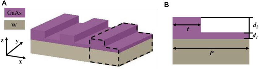
FIGURE 1. (A) Schematic of metal W-semiconductor GaAs structure of broadband absorber. (B) Cross-sectional view.
Our simulations and calculations use the finite-difference time-domain (FDTD)methods. The software used is FDTD solutions of Lumerical Company. Compared with other commercial simulation software, its calculation time is shorter and the accuracy is higher, which is very suitable for the simulation of nanostructure. In the actual simulation parameter setting, the incident light source is vertically incident from above the structure and adopts TM polarized plane wave. The boundary conditions are set by using periodic boundary conditions in the x-direction and perfect matched layer to cut off the boundary in the z direction. The division precision of the grid is 10 nm × 10 nm × 5 nm. The material parameters of metal W and semiconductor GaAs are used in the material library of the FDTD solutions software. The global absorption of the structure can be calculated with the formula A = 1-T-R, where the absorption is A, T and R represent the transmission and reflection, respectively (Long et al., 2016; Liu et al., 2017; Cai et al., 2019; Liu et al., 2021).
Results and Discussion
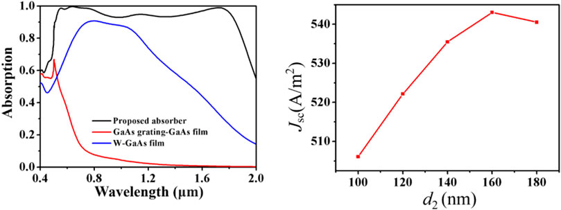
Figure 2 presents the simulation results of the structure. Obviously, the absorption effect of the proposed absorber is excellent, the absorption is higher than 90% at 500–1,850 nm. In order to reflect the rationality of the designed structure, we also calculated the other two similar configurations as a comparison. The absorption when there is no top grating and there is only a layer of W substrate and GaAs film is indicated by the blue line, and the red line represents the absorption when there is no W substrate and only GaAs film and grating. Clearly, when there is no top layer of GaAs grating, the structure only got a higher absorption at the wavelength from 700 to 1,100 nm, but there is almost no part higher than 90%, and the absorption at the wavelength after 1,100 nm drops rapidly; In the case of a non-metal W substrate, as shown by the red line, there is an absorption of about 60% only at the beginning of the curve, and thereafter it continues to decrease until it approaches zero. Through the comparison of the two, we can fully realize that the light reflection effect of the metal substrate and the LSPR mode excited by the top semiconductor grating have a huge effect on the improvement of the overall absorber, and the loss of any part of the component will lead to the collapse of the overall structure (Lv et al., 2018; Huang et al., 2021; Xu et al., 2021).
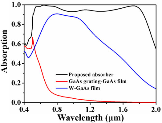
FIGURE 2. Absorption of broadband absorber in several different configurations.
There are many choices of metal and semiconductor materials. As a comparison, we listed the absorption of several other very common metal materials and semiconductors, as shown in Figure 3. Figure 3A presents the effect of choosing different metals when GaAs is used as the top layer material. In order to make a comprehensive comparison, we not only chose to use traditional noble metals such as gold and silver, but also selected Ti and V, which are the same refractory metals as W. It is very clear that the high absorption part of traditional noble metals is concentrated in the short wavelength region and the bandwidth is very narrow, and the absorption in the whole band is very unsatisfactory. This result is mainly caused by the small metal loss of noble metals (Cai et al., 2014). Figure 3B is the absorption spectrum of several different semiconductor materials when metal W is used as the bottom layer. It shows that GaAs is the best choice because of the widest absorption bandwidth and the best absorption. This is mainly because GaAs has a higher dielectric constant and the electromagnetic field has a strong excitation effect on the structure, so it has a good absorption effect.
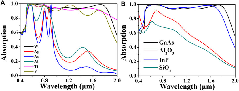
FIGURE 3. (A) Absorbance spectrum of different metal materials. (B) Absorbance spectrum of different semiconductor materials.
Further, we have investigated the influences of several main geometric parameters on the overall absorption effect one by one, which explains the reasons for the selection of geometric parameters of the proposed absorber, and we also simulated the tuning according to the needs of the actual use. First, we studied the influence of the total structure period P on absorption, as shown in Figure 4A. We calculated in the range of 400–600 nm with 50 nm steps. It is clear that with the increase of the period, in the main absorption band (>90% part), the overall absorption of the structure continues to increase, and the bandwidth does not change significantly. However, this increase is not unlimited. At P = 550 nm, the total absorption begins to decrease. This is because the excessively large period greatly increases the intensity of the surface plasmon resonance (Chen et al., 2019a; Chen et al., 2019b; Chen et al., 2018), which narrows the absorption bandwidth slightly and decreases the absorption. Therefore, after comprehensive consideration, we selected P = 500 nm, which is an ideal parameter. Subsequently, we simulated the influence of the width t of the grating on the absorption of the structure, and the result is presented in Figure 4B. Obviously, its main influence on the spectrum is reflected in the long wavelength range. When the width of the grating becomes wider, the global absorption bandwidth becomes obviously wider, but the change of the absorption rate is not same, it is a trend of first increasing and then decreasing. After exhaustive consideration, we finally select the middle parameter as the optimal value, so that a wider absorption bandwidth can be obtained without making the overall absorption too low.
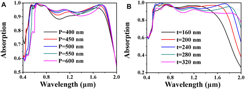
FIGURE 4. (A) Absorption spectrum under different periods. (B) Absorption spectrum under different grating widths.
After having investigated the influences of period and grating width on the whole absorption of the proposed absorber, we also studied the influence of grating layer and semiconductor layer thickness parameters on absorption, as results shown in Figure 5. First, we have changed the thickness of the semiconductor layer from 10 to 50 nm, and 10 nm as the step. We can see that the total absorption first rises from 10 nm, and reaches a maximum at 30 nm, then decreases as the height increases. The whole bandwidth is slightly widened as the height increases. 30 nm is selected as the optimal parameter on balance, so as not to make the bandwidth too narrow, but also to obtain the highest absorbance. Next, we also studied the influence of the different top grating layer thickness on absorption, and the results are presented in Figure 5B. The absorption of the structure is very low and the bandwidth is narrow when d2 = 40 nm; when it is increased to 80 nm, there is a big improvement. By comparison, we selected the optimal parameters 120 nm. In conclusion, whether it is the period of the structure, the width of the grating or the thickness of the semiconductor GaAs layer, the change of these parameters directly affects the surface plasmon resonance characteristics of the entire structure, or make it strengthen, or make it weaken, which in turn leads to a corresponding change in the absorption of the proposed absorber and the bandwidth of the spectrum (Chen et al., 2013; Liu et al., 2020; An et al., 2021; Cheng T. et al., 2021). The width of the top grating will not only affect the surface plasmon resonance, but also the change of its geometric parameters will have a certain effect on the cavity film of the structure, which will not be described in detail here.
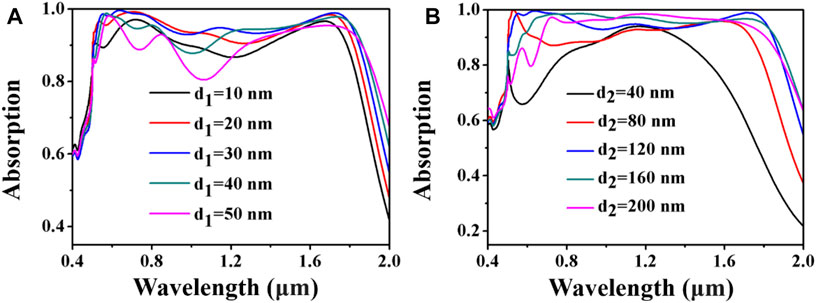
FIGURE 5. (A) Absorption spectrum with different semiconductor layer thicknesses. (B) Absorption spectrum with different grating layer thicknesses.
As a solar absorber will be applied in the actual environment, it can be expected that the light in nature cannot be incident perpendicularly as in the ideal case (Cheng et al., 2015). Therefore, we must take these factors into consideration when simulating. In fact, the absorption under oblique incidence and different polarization angles are also two important parameters for examining the structural design of the solar absorber. Figure 6A is the absorption spectrum when the incidence angle changes from 0 to 60°, and Figure 6B is the absorption spectrum when the polarization angle changes from 0 to 90°. It is obviously from Figure 6A that the total absorption effect of the proposed absorber is good at the long wavelength range. The absorption starts to decrease significantly as the incident angle is close to 60°. However, the result is not very ideal in the short wavelength range. When the incident angle begins to increase, not only the absorption decreases, but the high-efficiency absorption bandwidth also becomes narrow. As for the situation when the polarization angle is changed as shown in Figure 6B, when the rotation angle exceeds about 30°, the absorption and bandwidth of the structure will decrease significantly. This is because the structure is not completely symmetrical, and when switching to the TE polarization mode, the surface plasmon resonance cannot be excited. The simulation results are consistent with the theoretical explanation.
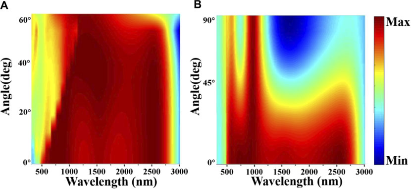
FIGURE 6. (A) Absorption at different incident angles. (B) Absorption at different polarization angles.
The proposed absorber is mainly used for solar energy collection. Therefore, its absorption characteristics in actual solar radiation are very important. We simulated carefully to test the performance in actual situation of the proposed absorber. The solar energy absorption efficiency equation with AM 1.5 is:
Where
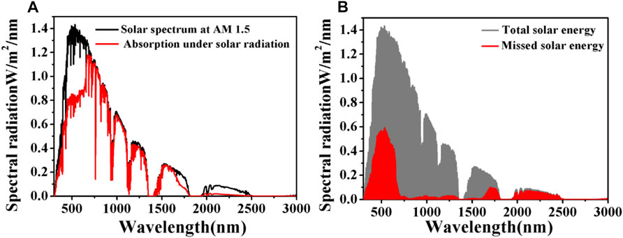
FIGURE 7. (A) Absorption spectrum under a solar spectrum at AM 1.5. (B) Total solar energy and missed energy at AM 1.5.
In the Figure 7A, black line is the solar spectrum at AM 1.5, red line is the absorption spectrum for the proposed absorber under solar radiation. It is very clear that the red line is much lower than the black line at the wavelength of 400–750 nm, which means the absorption of light in this range is relatively low. Also, the red line does not match the black line at the wavelength of 1,500–2,500 nm, which represents the low energy absorption same. In order to present this phenomenon intuitively, we made a schematic diagram showing the relationship between energy missed and total energy, as shown in Figure 7B. The gray area is the total solar energy, and the red area is the energy missed by the proposed absorber. We can see that the area of energy missed is also mainly concentrated in the two bands mentioned earlier, and the area is larger, which represents a greater loss of energy. Nevertheless, the global absorption effect of the proposed absorber is good and acceptable.
In practical applications, the proposed absorber can be used as a main component of a solar cell. Since it is a solar cell, the photoelectric conversion efficiency is a matter of great concern to us, and the photoelectric conversion efficiency is directly related to the ideal short-circuit current and directly proportional, which means that in order to achieve higher photoelectric conversion efficiency, higher short-circuit current is the basis (Ghasemi et al., 2014; Ni et al., 2016). Therefore, we studied the ideal short-circuit current of the structure and simulated with different grating layer thicknesses, as shown in Figure 8. When the grating layer thickness d2 = 160 nm, the short-circuit current reaches the maximum value, which is 543.027 A/m2.
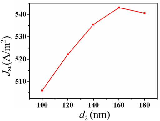
FIGURE 8. The influence of different grating layer thickness on short-circuit current.
Discussion
A broadband absorber structure based on metal W and semiconductor material GaAs is proposed in this paper. Its structure is very simple, consisting only of metal W substrate, GaAs film layer and grating layer. We have achieved broadband absorption at the wavelength of 500–1,850 nm by repeatedly adjusting the geometric parameters. Subsequently, the rationality of its structure design and materials selection, the influences of several geometric parameters on the global structure, the spectrum when incident and polarization angle change, the solar absorption and loss spectrum, and the ideal short-circuit current are analyzed one by one. We mainly drew the following conclusions:
1) The reflection effect of the metal substrate on the light and the LSPR mode excited by the top semiconductor grating have a very clear effect on the improvement of the total absorber, and the absence of any part will result in the failure of broadband absorption.
2) Selecting noble metals with less metal loss as the film will narrow the bandwidth; among semiconductor materials, GaAs has a stronger electrical excitation due to its higher dielectric constant, so the broadband absorption effect is good.
3) The change of the geometric parameters of the structure actually affects the surface plasmon resonance of the structure, and then different absorption conditions will appear.
Data Availability Statement
The original contributions presented in the study are included in the article/Supplementary Material, further inquiries can be directed to the corresponding authors.
Author Contributions
All authors listed have made a substantial, direct, and intellectual contribution to the work and approved it for publication.
Funding
This work is supported by the National Natural Science Foundation of China (11774128, 11704223), and the Natural Science Foundation of Shandong Province (ZR2018JL003, 2019KJJ003).
Conflict of Interest
The authors declare that the research was conducted in the absence of any commercial or financial relationships that could be construed as a potential conflict of interest.
Publisher’s Note
All claims expressed in this article are solely those of the authors and do not necessarily represent those of their affiliated organizations, or those of the publisher, the editors and the reviewers. Any product that may be evaluated in this article, or claim that may be made by its manufacturer, is not guaranteed or endorsed by the publisher.
References
An, S., Hu, C., Zhou, L., Yi, Z., Liu, C., Lv, J., et al. (2021). Design of Broadband Single-Polarization Filter Based on Simple Structure Photonic crystal Fiber with Gold-Coated Air Holes. Mod. Phys. Lett. B. 35 (30), 2150473. doi:10.1142/S021798492150473X
Briggs, R. M., Pryce, I. M., and Atwater, H. A. (2010). Compact Silicon Photonic Waveguide Modulator Based on the Vanadium Dioxide Metal-Insulator Phase Transition. Opt. Express 18 (11), 11192–11201. doi:10.1364/OE.18.011192
Cai, L., Zhang, Z., Xiao, H., Chen, S., and Fu, J. (2019). An Eco-Friendly Imprinted Polymer Based on Graphene Quantum Dots for Fluorescent Detection of P-Nitroaniline. RSC Adv. 9, 41383–41391. doi:10.1039/c9ra08726e
Cai, R., Rao, W., Zhang, Z., Long, F., and Yin, Y. (2014). An Imprinted Electrochemical Sensor for Bisphenol A Determination Based on Electrodeposition of a Graphene and Ag Nanoparticle Modified Carbon Electrode. Anal. Methods 6, 1590–1597. doi:10.1039/c3ay42125b
Cao, G., Li, H., Deng, Y., Zhan, S., He, Z., and Li, B. (2014). Systematic Theoretical Analysis of Selective-Mode Plasmonic Filter Based on Aperture-Side-Coupled Slot Cavity. Plasmonics 9, 1163–1169. doi:10.1007/s11468-014-9727-y
Chen, H.-J., Zhang, Z.-H., Cai, R., Kong, X.-Q., Chen, X., Liu, Y.-N., et al. (2013). Molecularly Imprinted Electrochemical Sensor Based on a Reduced Graphene Modified Carbon Electrode for Tetrabromobisphenol A Detection. Analyst 138, 2769–2776. doi:10.1039/c3an00146f
Chen, J., Nie, H., Tang, C., Cui, Y., Yan, B., Zhang, Z., et al. (2019a). Highly Sensitive Refractive-Index Sensor Based on strong Magnetic Resonance in Metamaterials. Appl. Phys. Express 12, 052015. doi:10.7567/1882-0786/ab14fa
Chen, J., Peng, C., Qi, S., Zhang, Q., Tang, C., Shen, X., et al. (2018). Photonic Microcavity-Enhanced Magnetic Plasmon Resonance of Metamaterials for Sensing Applications. IEEE Photon. Technol. Lett. 31 (2), 113–116. doi:10.1109/LPT.2018.2881989
Chen, J., Qi, S., Hong, X., Gu, P., Wei, R., Tang, C., et al. (2019b). Highly Sensitive 3D Metamaterial Sensor Based on Diffraction Coupling of Magnetic Plasmon Resonances. Results Phys. 15, 102791. doi:10.1016/j.rinp.2019.102791
Chen, P., Liu, F., Ding, H., Chen, S., Chen, L., Li, Y.-J., et al. (2019). Porous Double-Shell CdS@C3N4 Octahedron Derived by In Situ Supramolecular Self-Assembly for Enhanced Photocatalytic Activity. Appl. Catal. B Environ. 252, 33–40. doi:10.1016/j.apcatb.2019.04.006
Chen, Z., Chen, H., Jile, H., Xu, D., Yi, Z., Lei, Y., et al. (2021b). Multi-band Multi-Tunable Perfect Plasmon Absorber Based on L-Shaped and Double-Elliptical Graphene Stacks. Diamond Relat. Mater. 115, 108374. doi:10.1016/j.diamond.2021.108374
Chen, Z., Chen, H., Yin, J., Zhang, R., Jile, H., Xu, D., et al. (2021a). Multi-band, Tunable, High Figure of merit, High Sensitivity Single-Layer Patterned Graphene-Perfect Absorber Based on Surface Plasmon Resonance. Diamond Relat. Mater. 116, 108393. doi:10.1016/j.diamond.2021.108393
Cheng, T., Gao, H., Li, R., Wang, S., Yi, Z., and Yang, H. (2021). Flexoelectricity-induced Enhancement in Carrier Separation and Photocatalytic Activity of a Photocatalyst. Appl. Surf. Sci. 566, 150669. doi:10.1016/j.apsusc.2021.150669
Cheng, T., Gao, H., Liu, G., Pu, Z., Wang, S., Yi, Z., et al. (2022). Preparation of Core-Shell Heterojunction Photocatalysts by Coating CdS Nanoparticles onto Bi4Ti3O12 Hierarchical Microspheres and Their Photocatalytic Removal of Organic Pollutants and Cr(VI) Ions. Colloids Surf. A Physicochem. Eng. Asp. 633 (2), 127918. doi:10.1016/j.colsurfa.2021.127918
Cheng, Z., Liao, J., He, B., Zhang, F., Zhang, F., Huang, X., et al. (2015). One-Step Fabrication of Graphene Oxide Enhanced Magnetic Composite Gel for Highly Efficient Dye Adsorption and Catalysis. ACS Sust. Chem. Eng. 3, 1677–1685. doi:10.1021/acssuschemeng.5b00383
Deng, Y., Cao, G., Wu, Y., Zhou, X., and Liao, W. (2015). Theoretical Description of Dynamic Transmission Characteristics in MDM Waveguide Aperture-Side-Coupled with Ring Cavity. Plasmonics 10, 1537–1543. doi:10.1007/s11468-015-9971-9
Deng, Y., Cao, G., Yang, H., Zhou, X., and Wu, Y. (2018). Dynamic Control of Double Plasmon-Induced Transparencies in Aperture-Coupled Waveguide-Cavity System. Plasmonics 13, 345–352. doi:10.1007/s11468-017-0519-z
Fu, H., Yi, Z., Shi, Y., Liu, C., Lv, J., Yang, L., et al. (2021). Circular Anti-resonance Fibre Supporting Orbital Angular Momentum Modes with Flat Dispersion, High Purity and Low Confinement Loss. J. Mod. Opt. 68 (15), 784–791. doi:10.1080/09500340.2021.1947533
Ghasemi, H., Ni, G., Marconnet, A. M., Loomis, J., Yerci, S., Miljkovic, N., et al. (2014). Solar Steam Generation by Heat Localization. Nat. Commun. 5, 4449. doi:10.1038/ncomms5449
Huang, M., Wei, K., Wu, P., Xu, D., and Xu, Y. (2021). Design of Grating Type GaAs Solar Absorber and Investigation of its Photoelectric Characteristics. Front. Mater. 8, 781803. doi:10.3389/fmats.2021.781803
Jiang, L., Yi, Y., Tang, Y., Li, Z., Yi, Z., Liu, L., et al. (2021a). A High Quality Factor Ultra-narrow Band Perfect Metamaterial Absorber for Monolayer Molybdenum Disulfide. Chin. Phys. B. 19, 103415. doi:10.1088/1674-1056/ac1e11
Jiang, L., Yuan, C., Li, Z., Su, J., Yi, Z., Yao, W., et al. (2021b). Multi-Band and High-Sensitivity Perfect Absorber Based on Monolayer Graphene Metamaterial. Diamond Relat. Mater. 111, 108227. doi:10.1016/j.diamond.2020.108227
Khavasi, A. (2015). Design of Ultra-Broadband Graphene Absorber Using Circuit Theory. J. Opt. Soc. Am. B. 32 (9), 1941. doi:10.1364/JOSAB.32.001941
Kimpton, H., Stulz, E., and Zhang, X. (2020). Silver Nanofluids Based Broadband Solar Absorber Through Tuning Nanosilver Geometries. Solar Energy 208, 515–526. doi:10.1016/j.solener.2020.08.018
Lei, J., Ji, B., and Lin, J. (2016). High-Performance Tunable Plasmonic Absorber Based on the Metal-Insulator-Metal Grating Nanostructure. Plasmonics 12 (1), 151–156. doi:10.1007/s11468-016-0242-1
Li, J., Chen, X., Yi, Z., Yang, H., Tang, Y., Yi, Y., et al. (2020a). Broadband Solar Energy Absorber Based on Monolayer Molybdenum Disulfide Using Tungsten Elliptical Arrays. Mater. Today Energ. 16, 100390. doi:10.1016/j.mtener.2020.100390
Li, J., Jiang, J., Xu, Z., Liu, M., Tang, S., Yang, C., et al. (2018). Facile Synthesis of Ag@Cu2O Heterogeneous Nanocrystals Decorated N-Doped Reduced Graphene Oxide with Enhanced Electrocatalytic Activity for Ultrasensitive Detection of H2O2. Sens. Actuators B: Chem. 260, 529–540. doi:10.1016/j.snb.2018.01.068
Li, J., Jiang, J., Zhao, D., Xu, Z., Liu, M., Liu, X., et al. (2020b). Novel Hierarchical Sea Urchin-Like Prussian Blue@palladium Core-Shell Heterostructures Supported on Nitrogen-Doped Reduced Graphene Oxide: Facile Synthesis and Excellent Guanine Sensing Performance. Electrochim. Acta 330, 135196. doi:10.1016/j.electacta.2019.135196
Li, R., Zheng, Y., Luo, Y., Zhang, J., Yi, Z., Liu, L., et al. (2021). Multi-Peak Narrow-Band Perfect Absorber Based on Two-Dimensional Graphene Array. Diamond Relat. Mater. 120, 108666. doi:10.1016/j.diamond.2021.108666
Li, Y., Li, M., Xu, P., Tang, S., and Liu, C. (2016). Efficient Photocatalytic Degradation of Acid orange 7 over N-Doped Ordered Mesoporous Titania on Carbon Fibers under Visible-Light Irradiation Based on Three Synergistic Effects. Appl. Catal. A: Gen. 524, 163–172. doi:10.1016/j.apcata.2015.01.050
Li, Z., Yi, Y., Xu, D., Yang, H., Yi, Z., Chen, X., et al. (2021b). A Multi-Band and Polarization-Independent Perfect Absorber Based on Dirac Semimetals Circles and Semi-ellipses Array. Chin. Phys. B. 30, 098102. doi:10.1088/1674-1056/abfb57
Li, Z., Yi, Z., Liu, T., Liu, L., Chen, X., Zheng, F., et al. (2021a). Three-Band Perfect Absorber with High Refractive Index Sensing Based on an Active Tunable Dirac Semimetal. Phys. Chem. Chem. Phys. 23 (32), 17374–17381. doi:10.1039/D1CP01375K
Li-Ying, J., Yi, Y. T., Ying-Ting, Y., Zao, Y., Hua, Y., Zhi-You, L., et al. (2021). A Four-Band Perfect Absorber Based on High Quality Factor and High Quality Factor of Monolayer Molybdenum Disulfide. Acta Phys. Sin. 70, 128101. doi:10.7498/aps.70.20202163
Liu, H., Wang, Q., and Zhang, F. (2020). Preparation of Fe3O4@SiO2@ P(AANa-co-AM) Composites and Their Adsorption for Pb(II). ACS Omega 5, 8816–8824. doi:10.1021/acsomega.0c00403
Liu, W., Shi, Y., Yi, Z., Liu, C., Wang, F., Li, X., et al. (2021). Surface Plasmon Resonance Chemical Sensor Composed of a Microstructured Optical Fiber for the Detection of an Ultra-Wide Refractive index Range and Gas-Liquid Pollutants. Opt. Express 29 (25), 40734–40747. doi:10.1364/oe.444323
Liu, Y., Bo, M., Yang, X., Zhang, P., Sun, C. Q., and Huang, Y. (2017). Size Modulation Electronic and Optical Properties of Phosphorene Nanoribbons: DFT-BOLS Approximation. Phys. Chem. Chem. Phys. 19, 5304–5309. doi:10.1039/c6cp08011a
Long, F., Zhang, Z. H., Wang, J., Yan, L., Lu, P. P., and Yang, Z. X. (2016). Magnetic Graphene Modified Imprinted Electrochemical Sensor for Detection of 4-Octylphenol. Chin. J. Anal. Chem. 44, 908–914. doi:10.11895/j.issn.0253.3820.160016
Long, F., Zhang, Z., Wang, J., Yan, L., and Zhou, B. (2015). Cobalt-nickel Bimetallic Nanoparticles Decorated Graphene Sensitized Imprinted Electrochemical Sensor for Determination of Octylphenol. Electrochimica Acta 168, 337–345. doi:10.1016/j.electacta.2015.04.054
Lv, P., Xie, D., and Zhang, Z. (2018). Magnetic Carbon Dots Based Molecularly Imprinted Polymers for Fluorescent Detection of Bovine Hemoglobin. Talanta 188, 145–151. doi:10.1016/j.talanta.2018.05.068
Ni, G., Li, G., Boriskina, S. V., Li, H., Yang, W., Zhang, T., et al. (2016). Steam Generation under One Sun Enabled by a Floating Structure with thermal Concentration. Nat. Energ. 1, 16126. doi:10.1038/NENERGY.2016.126
Qin, F., Chen, X., Yi, Z., Yao, W., Yang, H., Tang, Y., et al. (2020). Ultra-Broadband and Wide-Angle Perfect Solar Absorber Based on TiN Nanodisk and Ti Thin Film Structure. Solar Energ. Mater. Solar Cell 211, 110535. doi:10.1016/j.solmat.2020.110535
Sobhani, A., Knight, M. W., Wang, Y., Zheng, B., King, N. S., Brown, L. V., et al. (2013). Narrowband Photodetection in the Near-Infrared with a Plasmon-Induced Hot Electron Device. Nat. Commun. 4, 1643. doi:10.1038/ncomms2642
Su, J., Yang, H., Xu, Y., Tang, Y., Yi, Z., Zheng, F., et al. (2021). Based on Ultrathin PEDOT:PSS/c-Ge Solar Cells Design and Their Photoelectric Performance. Coatings 11 (7), 748. doi:10.3390/coatings11070748
Tang, N., Li, Y., Chen, F., and Han, Z. (2018). In Situ fabrication of a Direct Z-Scheme Photocatalyst by Immobilizing CdS Quantum Dots in the Channels of Graphene-Hybridized and Supported Mesoporous Titanium Nanocrystals for High Photocatalytic Performance under Visible Light. RSC Adv. 8, 42233–42245. doi:10.1039/c8ra08008a
Wang, Y., Yi, Y., Xu, D., Yi, Z., Li, Z., Chen, X., et al. (2021). Terahertz Tunable Three Band Narrowband Perfect Absorber Based on Dirac Semimetal. Phys. E: Low-Dimens. Syst. Nanostructures 131, 114750. doi:10.1016/j.physe.2021.114750
Wu, X., Zheng, Y., Luo, Y., Zhang, J., Yi, Z., Wu, X., et al. (2021). A Four-Band and Polarization-Independent BDS-Based Tunable Absorber with High Refractive index Sensitivity. Phys. Chem. Chem. Phys. 23, 26864–26873. doi:10.1039/D1CP04568G
Xiao, L., Youji, L., Feitai, C., Peng, X., and Ming, L. (2017). Facile Synthesis of Mesoporous Titanium Dioxide Doped by Ag-Coated Graphene with Enhanced Visible-Light Photocatalytic Performance for Methylene Blue Degradation. RSC Adv. 7, 25314–25324. doi:10.1039/c7ra02198d
Xiao, L., Zhang, Q., Chen, P., Chen, L., Ding, F., Tang, J., et al. (2019). Copper-Mediated Metal-Organic Framework as Efficient Photocatalyst for the Partial Oxidation of Aromatic Alcohols under Visible-Light Irradiation: Synergism of Plasmonic Effect and Schottky junction. Appl. Catal. B: Environ. 248, 380–387. doi:10.1016/j.apcatb.2019.02.012
Xiong, S., Yin, Z., Zhou, Y., Peng, X., Yan, W., Liu, Z., et al. (2013). The Dual-Frequency (20/40 kHz) Ultrasound Assisted Photocatalysis with the Active Carbon Fiber-Loaded Fe3+-TiO2as Photocatalyst for Degradation of Organic Dye. Bull. Korean Chem. Soc. 34, 3039–3045. doi:10.5012/bkcs.2013.34.10.3039
Xu, F., Lin, L., Wei, D., Xu, J., and Fang, J. (2021). An Asymmetric Silicon Grating Dual-Narrow-Band Perfect Absorber Based on Dielectric-Metal-Dielectric Structure. Front. Mater. 8, 752745. doi:10.3389/fmats.2021.752745
Yang, X., Zhang, F., Hu, Y. J., Chen, D. Z., He, Z. Q., and Xiong, L. Z. (2014). Gold Nanoparticals Doping Graphene Sheets Nanocomposites Sensitized Screen-Printed Carbon Electrode as a Disposable Platform for Voltammetric Determination of Guaiacol in Bamboo Juice. Int. J. Electrochem. Sci. 9, 5061–5072.
Yi, Z., Li, J., Lin, J., Qin, F., Chen, X., Yao, W., et al. (2020). Broadband Polarization-Insensitive and Wide-Angle Solar Energy Absorber Based on Tungsten Ring-Disc Array. Nanoscale 12, 23077–23083. doi:10.1039/d0nr04502k
Yu, P., Yang, H., Chen, X., Yi, Z., Yao, W., Chen, J., et al. (2020). Ultra-Wideband Solar Absorber Based on Refractory Titanium Metal. Renew. Energ. 158, 227–235. doi:10.1016/j.renene.2020.05.142
Zhang, F., Wang, B., and Shen, Y. (2014). Blue Luminescent ZnO Nanoclusters Stabilized by Esterifiable Polyamidoamine Dendrimers and Their UV-Shielding Applications. Asian J. Chem. 26, 3467–3470. doi:10.14233/ajchem.2014.15942
Zhang, Z., Cai, R., Long, F., and Wang, J. (2015). Development and Application of Tetrabromobisphenol A Imprinted Electrochemical Sensor Based on Graphene/carbon Nanotubes Three-Dimensional Nanocomposites Modified Carbon Electrode. Talanta 134, 435–442. doi:10.1016/j.talanta.2014.11.040
Zhao, F., Chen, X., Yi, Z., Qin, F., Tang, Y., Yao, W., et al. (2020). Study on the Solar Energy Absorption of Hybrid Solar Cells with Trapezoid-Pyramidal Structure Based PEDOT:PSS/c-Ge. Solar Energy 204, 635–643. doi:10.1016/j.solener.2020.05.030
Zhao, F., Yi, Y., Lin, J., Yi, Z., Qin, F., Zheng, Y., et al. (2021). The Better Photoelectric Performance of Thin-Film TiO2/c-Si Heterojunction Solar Cells Based on Surface Plasmon Resonance. Results Phys. 28, 104628. doi:10.1016/j.rinp.2021.104628
Keywords: solar energy absorber, ultra-broadband perfect absorption, GaAs grating, photoelectric performance, surface plasmon resonance
Citation: Liu B, Wu P, Li Y, Zhu H and Lv L (2022) Design and Photoelectric Performance of Perfect Solar Absorber Based on GaAs Grating. Front. Mater. 8:821431. doi: 10.3389/fmats.2021.821431
Received: 24 November 2021; Accepted: 06 December 2021;
Published: 18 January 2022.
Edited by:
Hua Yang, Lanzhou University of Technology, ChinaReviewed by:
Chao Liu, Northeast Petroleum University, ChinaJing Chen, Nanjing University of Posts and Telecommunications, China
Yougen Yi, Central South University, China
Copyright © 2022 Liu, Wu, Li, Zhu and Lv. This is an open-access article distributed under the terms of the Creative Commons Attribution License (CC BY). The use, distribution or reproduction in other forums is permitted, provided the original author(s) and the copyright owner(s) are credited and that the original publication in this journal is cited, in accordance with accepted academic practice. No use, distribution or reproduction is permitted which does not comply with these terms.
*Correspondence: Hongyang Zhu, emh1aG9uZ3lhbmdAbHl1LmVkdS5jbg==; Li Lv, bGJfbHl1QDE2My5jb20=