 Feng Xu
 Jun Fang
- College of Chemical Engineering and Materials Science, Quanzhou Normal University, Quanzhou, China
With the exhaustion of world energy, new energy has become the most important content of each country’s development strategy. How to efficiently use solar energy has become a research hotspot in current scientific research. Based on surface plasmon resonance and Fabry-Perot (FP) cavity, this paper proposes a design method of asymmetric silicon grating absorber, and uses finite difference time domain (FDTD) method for simulation calculation. By adjusting the geometric parameters, the asymmetric silicon grating absorber realizes two narrow-band absorption peaks with absorption greater than 99% in the optical wavelength range of 3,000–5,000 nm, and the absorption peak wavelengths are λ1 = 3,780 nm and λ2 = 4,135 nm, respectively. When the electromagnetic wave is incident on the surface of the metamaterial, it will excite the plasmon resonance of the metal to form a surface plasmon (SP) wave. When the SP wave propagates along the x axis, the silicon grating can reflect the SP wave back and forth. When the frequency of the SP wave and the incident light are equal, it will cause horizontal FP coupling resonance, resulting in different resonance wavelengths. This paper also discusses the influence of geometric parameters, incident angle and polarization angle on the performance of silicon grating absorbers. Finally, the sensing performance of the structure as a refractive index sensor is studied. The absorber can be used for various spectral applications such as photon detection, optical filtering and spectral sensing.
Introduction
Surface plasmon resonance (SPR) is a non-radiative electromagnetic mode formed by the coupling of incident photons and free electrons on the metal surface (Cao et al., 2014). It is an excited state that locally propagates on the medium and metal surface. It is limited to the surface of the medium and metal, where the surface intensity is the highest, and it gradually attenuates to both sides in the direction perpendicular to the surface (Deng et al., 2015; Chen et al., 2021a; Li-Ying et al., 2021). Its propagation characteristics are related to the incident light source, the metal medium material and the surrounding refractive index (Jiang et al., 2021a). SPR provides a foundation for micro-nano applications due to its unique advantages, including biosensing, light field enhancement, solar cells, photocatalysis, Raman enhanced detection, and photodetectors (Liu et al., 2017; Xiao et al., 2017; Li et al., 2018; Chen et al., 2019; Li et al., 2020a; Zhao et al., 2021).
Resonance in subwavelength periodic structures has been studied extensively in the last decade. The resonance mode can be excited by the plasmon to affect the transmission, reflection and absorption characteristics of the structure (Ding and Magnusson, 2004; Deng et al., 2018; Jiang et al., 2021b). The near unit absorption of waves is called perfect absorption, and researchers have carried out many studies on perfect metamaterial absorbers (Cheng and Du, 2019; Cheng et al., 2019; Cheng et al., 2020; Cheng et al., 2021). They have many potential applications. Perfect absorbers with wide operating bandwidth are conducive to the application in photon detection, solar energy collection and other fields (Zhu et al., 2014; Rosenberg et al., 2019; Li et al., 2020b; Li et al., 2021a; Li et al., 2021b; Zhou et al., 2021), while perfect absorbers with narrow operating bandwidth have great advantages in sensing, filtering and selective thermal emission (Liu et al., 2010; Mason et al., 2011; Yi et al., 2020; Chen et al., 2021b; Wang et al., 2021). In addition, the ultra-narrow bandwidth refractive index sensor based on the perfect absorber has large figure of merit (FOM), and many researchers have proposed such a sensor with good performance (Vafapour and Ghahraloud, 2018; Keshavarz and Vafapour, 2019; Vafapour, 2019; Zhang et al., 2021). Usually, an all-metal structure or a three-layer or multi-layer metal insulator metal (MIM) structure is used to achieve perfect absorption in a narrow band (El-Gohary et al., 2014; Long et al., 2015; Zhang et al., 2015; Long et al., 2016; Elshorbagy et al., 2017). However, due to the incompatibility of these structures with complementary metal oxide semiconductor (CMOS) manufacturing processes, the manufacturing costs are high (Kuznetsov et al., 2016). Therefore, people are paying more and more attention to the realization of narrow-band perfect absorber through the dielectric structure on the metal system (Sharon et al., 1997; Liao and Zhao, 2017; Ren et al., 2019). Compared with the perfect metal absorber, this absorber can save manufacturing costs (Cui et al., 2014). This type of absorber usually has a dielectric waveguide layer. They can produce ultra-narrow absorption, but the structures are complex. Therefore, in order to optimize the structure, we can place the dielectric waveguide layer on the metal substrate or metal base film. For example, in 2016, Callewaert et al. proposed a narrow-band absorber based on a silver film dielectric nanodisk array (Callewaert et al., 2016).
In this paper, an asymmetric silicon grating absorber is designed based on the medium-metal-medium structure. Through the adjustment of geometric parameters, the dual-narrow-band perfect absorption is finally achieved. Asymmetric silicon grating is designed by using three unevenly spaced silicon strips in each cell. This asymmetric structure makes the absorber support horizontal FP resonance. The plane plasmon wave excited by the TM polarization (incident electric field polarized along the x-axis) incident can produce different FP coupling resonances with the incident light, resulting in two absorption peaks. When the incident angle is changed, the two absorption peaks show insensitive characteristics in the range of 0˚–20˚. In addition, the influence of geometric parameters and polarization angle on the performance of the absorber are briefly discussed. Finally, when this structure is used as a sensor, it has high sensitivity and quasi-linear response. It can be used in a variety of multi-spectral applications, such as filtering, photon detection, and spectral sensing.
Materials and Methods
Figure 1 shows the structure of the dual-narrow-band grating absorber we designed. It is made of a quartz substrate and a silicon grating on the surface of a gold film. Incident light source is TM plane light wave, and the direction of light source is perpendicular to grating plane. The period of the grating is A, and there are three silicon gratings with unequal spacing in each period. The three silicon grating structures in a unit period make the grating as a whole asymmetrical structure. h1 represents the height of the silicon grating, h2 represents the height of the gold thin layer, w represents the width of the silicon grating, and d1 and d2 represent the center spacing of adjacent silicon gratings. The parameters of gold and silicon come from Palik (Palik, 1998), and the refractive index of quartz is 1.45. In the case of normal light wave incidence, we calculate the reflection (R), transmission (T) and absorption (A) as shown in Figure 2. The geometric parameters of the structure are A = 3,000 nm, h1 = 630 nm, h2 = 90 nm, w = 300 nm, d1 = 560 nm, and d2 = 880 nm, respectively. We can notice from Figure 2 that the range of the light waveband is 3,000–5,000 nm, where the T is basically zero. The first absorption peak that appears is named λ1 (λ1 = 3,780 nm), and its full width at half maximum (FWHM) is 40 nm. The second absorption peak, we named λ2 (λ2 = 4,135 nm, FWHM = 39 nm). The absorption of the two resonance peak wavelengths exceeds 99%.
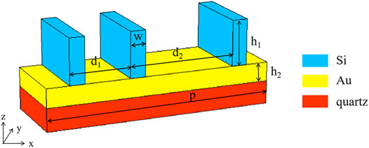
FIGURE 1. Three-dimensional structure diagram of asymmetric silicon grating.
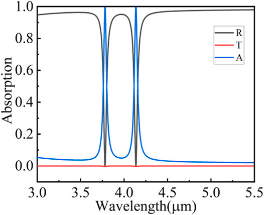
FIGURE 2. Spectra of reflection (R), transmission (T) and absorption (A) under normal incidence of TM polarized light.
Results and Discussion
In order to analyze the physical mechanism of resonance, we simulated and calculated the electric and magnetic field distributions at λ1 = 3,780 nm and λ2 = 4,135 nm on the XOZ plane. Figures 3A,B respectively show the electric field and magnetic field distribution at λ1. We have observed that the electric field is distributed at the top corners of the slits with small silicon grating spacing, and the magnetic field is mainly distributed between the slits with small silicon grating spacing. Figures 3C,D respectively show the electric field and magnetic field distribution at λ2. The difference from λ1 is that the electric field is distributed on the surface of the three silicon gratings, and the magnetic field is mainly distributed in the slits of the two silicon gratings with a larger silicon grating spacing. This indicates that these two resonance peaks are derived from the coupling between the SPR of the metal and the resonance of the FP cavity (Cheng et al., 2015; Lv et al., 2018; He et al., 2020). The resonant peak at λ1 is mainly related to the FP resonance between gratings with a short pitch (d1), and the resonant peak at λ2 is mainly derived from the FP resonance between gratings with a large pitch (d2).
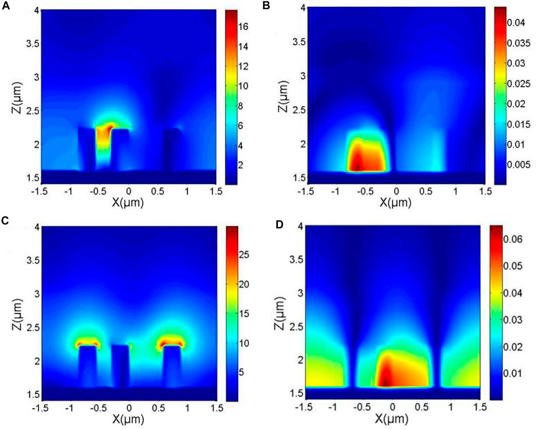
FIGURE 3. (A) and (B) represent the electric and magnetic field diagrams at λ1 = 3780 nm, respectively. (C) and (D) represent the electric and magnetic field diagrams at λ2 = 4135 nm, respectively.
Then in order to explore the influence of the asymmetric silicon grating structure on the absorption performance, we used the controlled variable method to change the geometric parameters. Figures 4A,B respectively show the influence of the change of the period and the geometric parameters of the silicon grating pitch on the absorption performance of the silicon grating. From Figure 4A, we can observe that as the period length increases, the first absorption peak (λ1) of the silicon grating gradually increases. With the increase of the period length, the two absorption peaks show red shift, and the longer the period length is, the farther the wavelength distance of the two absorption peaks is. At the same time, we noticed that the FWHM slowly decreases with the increase of the period. Figure 5B shows that we change the smaller silicon pitch of the asymmetric silicon grating (d1) as the geometric parameter variable. Through Figure 4B, we found that when the silicon grating pitch is 60 nm, the absorption of the two absorption peaks is not high, and the FWHM is large. As the spacing of the silicon grating increases, the absorption gradually increases, the FWHM gradually decreases, and the two absorption peaks appear blue shift. At the same time, we can observe that the change of the silicon grating pitch has a greater influence on the first absorption peak, indicating that the λ1 peak is sensitive to the change of the grating pitch, that is, the absorption peak is sensitive to the cavity length change.
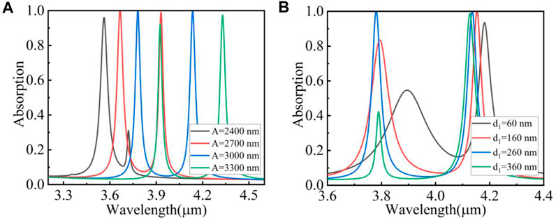
FIGURE 4. (A) The effect of changing the grating period on the absorption spectrum. (B) The effect of changing the smaller silicon pitch of the grating on the absorption spectrum.
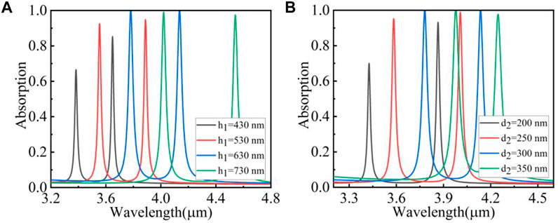
FIGURE 5. (A) The effect of changing the thickness of the grating silicon on the absorption spectrum. (B) The effect of changing the silicon width of the grating on the absorption spectrum.
Figures 5A,B respectively show the influence of asymmetric silicon grating thickness and silicon grating width geometric parameters (d2) on the absorption performance of the silicon grating. From Figure 5A, we can observe that as the thickness of the silicon grating increases, the absorption of the two absorption peaks shows a trend of first increasing and then decreasing. This is because when the thickness of the silicon grating is small, it weakens the FP resonance and reduces the absorption of light. When the thickness increases to a certain size (630 nm), that is, when the thickness reaches the critical value, the absorption will no longer increase. At the same time, both absorption peaks appear red shift. And the distance between the two absorption peaks gradually increases, because each silicon grating plays a different role in the FP cavity. From Figure 5B, we also found that as the width of the silicon grating increases, the two absorption peaks first increase and then decrease, the resonance wavelength appears red-shifted, and the FWHM gradually increases. However, unlike the trend of silicon grating thickness changes, as the silicon thickness changes, the distance between the two absorption peaks becomes smaller and smaller. The reason is the same as the thickness of the silicon grating: each silicon grating acts as a mirror, and their role is different.
In addition, we also studied the spectral response of the asymmetric silicon grating structure under different incident angles and polarization angles, and the results are shown in Figure 6. It can be seen that the intensity and position of the absorption peaks in the range of 0˚–20˚ incident angle do not change, which indicates that the absorber is not sensitive to the incident angle in this range. When the incident angle exceeds 20˚, the absorption will be greatly reduced due to the wave vector mismatch. When changing the polarization angle of the beam from 0°(TM polarization) to 90° (TE polarization), the results are shown in Figure 6B. It can be clearly found that the extinction intensity of the two peaks decreases with the increase of the polarization angle. At the same time, we also noticed that when the incident plane wave is TE polarization, two new resonance peaks appear, which are caused by phase resonance (Qin et al., 2020; Su et al., 2021). The electric field generated at this time has a phase difference of π, which causes the far field to produce coherent cancellation, thereby generating two new peaks.
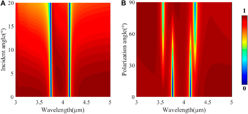
FIGURE 6. (A) The relation between resonance wavelength and incident angle under TM polarization. (B) The effect of changing the polarization angle of incident light on the reflection spectrum.
Finally, in order to explore the performance of asymmetric silicon grating as a refractive index sensor, we conduct research by changing its environmental refractive index. Figure 7A shows the absorption spectrum of the silicon grating when the refractive index of the surrounding environment changes. Since our silicon grating structure belongs to narrow-band absorption, we set the refractive index to change from 1.0 to 1.1 with a gradient of 0.02. From the figure, we can observe that as the refractive index of the environment increases, the two absorption peaks appear red-shifted, but the peaks of the two absorption peaks remain basically stable. At the same time, we found that the FWHM of the two absorption peaks did not change much, the change range was between 1 and 2nm, and we took the average value of the FWHM. Figures 7B,C show the corresponding absorption peak wavelengths of the two absorption peaks of λ1 and λ2 under the change of refractive index. The oblique line data is obtained by our linear fitting process. According to the formula S = ∆λ/∆n and FOM = S/FWHM, the sensitivity (S) and FOM of the silicon grating can be calculated (Chen et al., 2013; Cai et al., 2014; Tang et al., 2018; Wu et al., 2020; Chen et al., 2021c). According to the formula, we can find that the slope of the straight line is the S. The S of the absorption peaks at λ1 and λ2 are 2,500 nm/RIU and 3,000 nm/RIU. The FWHM are 40 nm and 39 nm. FOM are 62.5 and 76.9. It can be found that this structure has high sensitivity, so it can be applied in the field of refractive index sensors.
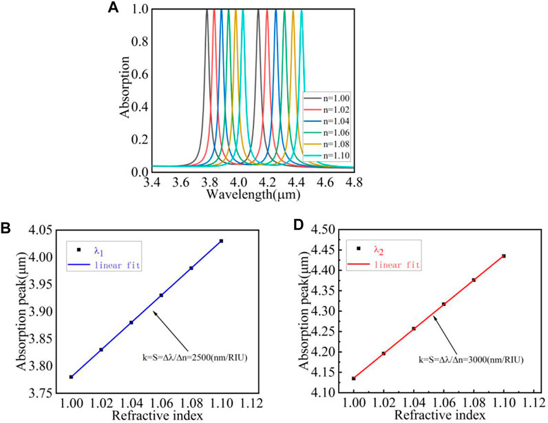
FIGURE 7. (A) When changing the environmental background refractive index, the absorption spectrum of the grating. (B) For the wavelength λ1, the peak wavelength relationship diagram corresponding to the refractive index change. (C) For the wavelength λ2, the peak wavelength relationship diagram corresponding to the refractive index change.
Conclusion
In conclusion, we fully demonstrate the absorption of dielectric structures on metal systems, based on the gold mold. By adjusting the geometric parameters, the asymmetric silicon grating absorber achieves the best absorption efficiency, two narrow-band absorption peaks in the range 3,000–5,000 nm light wave segments, the absorption peaks are λ1 = 3,780 nm and λ2 = 4,135 nm. And the absorption value is over 99%. We find that the distance between asymmetric gratings and the length of periods are changed, the absorption and FWHM of the absorption peak are the most affected. At the same time, it is found that the extinction intensity of the two peaks decreases with the increase of polarization angle. The structure has good sensing performance and high sensitivity. For the absorption peak of λ1, S = 2,500 nm/RIU and FOM = 62.5. For the absorption peak of λ2, S = 3,000 nm/RIU and FOM = 76.9.
Data Availability Statement
The original contributions presented in the study are included in the article/Supplementary Material, further inquiries can be directed to the corresponding author.
Author Contributions
FX: Conceptualization, Formal analysis, Investigation, Data curation, Writing-original draft, Writing-review and editing. LL: Conceptualization, Formal analysis, Investigation, Data curation, funding acquisition. DW: Conceptualization, Formal analysis, Investigation, Data curation, Writing-original draft, Writing-review and editing. JX: Conceptualization, Formal analysis, Revision. JF: Conceptualization, Formal analysis, Revision.
Funding
This work was supported by the National Natural Science Foundation of China (21676222, U175252), the Natural Science Foundation of Fujian Province (2019J01732, JT180365), the Quanzhou high level Talents Innovation and Entrepreneurship Project (2020C044R).
Conflict of Interest
The authors declare that the research was conducted in the absence of any commercial or financial relationships that could be construed as a potential conflict of interest.
Publisher’s Note
All claims expressed in this article are solely those of the authors and do not necessarily represent those of their affiliated organizations, or those of the publisher, the editors and the reviewers. Any product that may be evaluated in this article, or claim that may be made by its manufacturer, is not guaranteed or endorsed by the publisher.
References
Cai, R., Rao, W., Zhang, Z., Long, F., and Yin, Y. (2014). An Imprinted Electrochemical Sensor for Bisphenol A Determination Based on Electrodeposition of a Graphene and Ag Nanoparticle Modified Carbon Electrode. Anal. Methods 6, 1590–1597. doi:10.1039/c3ay42125b
Callewaert, F., Chen, S., Butun, S., and Aydin, K. (2016). Narrow Band Absorber Based on a Dielectric Nanodisk Array on Silver Film. J. Opt. 18 (7), 075006. doi:10.1088/2040-8978/18/7/075006
Cao, G., Li, H., Deng, Y., Zhan, S., He, Z., and Li, B. (2014). Systematic Theoretical Analysis of Selective-Mode Plasmonic Filter Based on Aperture-Side-Coupled Slot Cavity. Plasmonics 9, 1163–1169. doi:10.1007/s11468-014-9727-y
Chen, H.-J., Zhang, Z.-H., Cai, R., Kong, X.-Q., Chen, X., Liu, Y.-N., et al. (2013). Molecularly Imprinted Electrochemical Sensor Based on a Reduced Graphene Modified Carbon Electrode for Tetrabromobisphenol A Detection. Analyst 138, 2769–2776. doi:10.1039/c3an00146f
Chen, P., Liu, F., Ding, H., Chen, S., Chen, L., Li, Y.-J., et al. (2019). Porous Double-Shell CdS@C3N4 Octahedron Derived by In Situ Supramolecular Self-Assembly for Enhanced Photocatalytic Activity. Appl. Catal. B: Environ. 252, 33–40. doi:10.1016/j.apcatb.2019.04.006
Chen, X., Wu, W., Zhang, W., Wang, Z., Fu, Z., Zhou, L., et al. (2021). Blue and green Double Band Luminescent Carbon Quantum Dots: Synthesis, Origin of Photoluminescence, and Application in white Light-Emitting Devices. Appl. Phys. Lett. 118, 153102. doi:10.1063/5.0046495
Chen, Z., Chen, H., Jile, H., Xu, D., Yi, Z., Lei, Y., et al. (2021). Multi-band Multi-Tunable Perfect Plasmon Absorber Based on L-Shaped and Double-Elliptical Graphene Stacks. Diamond Relat. Mater. 115, 108374. doi:10.1016/j.diamond.2021.108374
Chen, Z., Chen, H., Yin, J., Zhang, R., Jile, H., Xu, D., et al. (2021). Multi-band, Tunable, High Figure of merit, High Sensitivity Single-Layer Patterned Graphene-Perfect Absorber Based on Surface Plasmon Resonance. Diamond Relat. Mater. 116, 108393. doi:10.1016/j.diamond.2021.108393
Cheng, Y., Chen, F., and Luo, H. (2021). Plasmonic Chiral Metasurface Absorber Based on Bilayer Fourfold Twisted Semicircle Nanostructure at Optical Frequency. Nanoscale Res. Lett. 16, 12. doi:10.1186/s11671-021-03474-6
Cheng, Y., Chen, F., and Luo, H. (2020). Triple-Band Perfect Light Absorber Based on Hybrid Metasurface for Sensing Application. Nanoscale Res. Lett. 15 (1), 103. doi:10.1186/s11671-020-03332-x
Cheng, Y., and Du, C. (2019). Broadband Plasmonic Absorber Based on All Silicon Nanostructure Resonators in Visible Region. Opt. Mater. 98, 109441. doi:10.1016/j.optmat.2019.109441
Cheng, Y., Luo, H., Chen, F., and Gong, R. (2019). Triple Narrow-Band Plasmonic Perfect Absorber for Refractive index Sensing Applications of Optical Frequency. OSA Continuum 2 (7), 2113. doi:10.1364/osac.2.002113
Cheng, Z., Liao, J., He, B., Zhang, F., Zhang, F., Huang, X., et al. (2015). One-Step Fabrication of Graphene Oxide Enhanced Magnetic Composite Gel for Highly Efficient Dye Adsorption and Catalysis. ACS Sust. Chem. Eng. 3, 1677–1685. doi:10.1021/acssuschemeng.5b00383
Cui, Y., He, Y., Jin, Y., Ding, F., Yang, L., Ye, Y., et al. (2014). Plasmonic and Metamaterial Structures as Electromagnetic Absorbers. Laser Photon. Rev. 8, 495–520. doi:10.1002/lpor.201400026
Deng, Y., Cao, G., Wu, Y., Zhou, X., and Liao, W. (2015). Theoretical Description of Dynamic Transmission Characteristics in MDM Waveguide Aperture-Side-Coupled with Ring Cavity. Plasmonics 10, 1537–1543. doi:10.1007/s11468-015-9971-9
Deng, Y., Cao, G., Yang, H., Zhou, X., and Wu, Y. (2018). Dynamic Control of Double Plasmon-Induced Transparencies in Aperture-Coupled Waveguide-Cavity System. Plasmonics 13, 345–352. doi:10.1007/s11468-017-0519-z
Ding, Y., and Magnusson, R. (2004). Resonant Leaky-Mode Spectral-Band Engineering and Device Applications. Opt. Express 12 (23), 5661–5674. doi:10.1364/opex.12.005661
El-Gohary, S. H., Choi, J. M., Kim, N.-H., and Byun, K. M. (2014). Plasmonic Metal-Dielectric-Metal Stack Structure with Subwavelength Metallic Gratings for Improving Sensor Sensitivity and Signal Quality. Appl. Opt. 53, 2152–2157. doi:10.1364/ao.53.002152
Elshorbagy, M. H., Cuadrado, A., and Alda, J. (2017). High-sensitivity Integrated Devices Based on Surface Plasmon Resonance for Sensing Applications. Photon. Res. 5, 654–661. doi:10.1364/prj.5.000654
He, X., Jie, J., Yang, J., Han, Y., and Zhang, S. (2020). Asymmetric Dielectric Grating on Metallic Film Enabled Dual- and Narrow-Band Absorbers. Opt. Express 28 (4), 4594–4602. doi:10.1364/oe.386742
Jiang, L., Yi, Y., Tang, Y., Li, Z., Yi, Z., Liu, L., et al. (2021). A High Quality Factor Ultra-narrow Band Perfect Metamaterial Absorber for Monolayer Molybdenum Disulfide. Chin. Phys. B 19, 103415. doi:10.1088/1674-1056/ac1e11
Jiang, L., Yuan, C., Li, Z., Su, J., Yi, Z., Yao, W., et al. (2021). Multi-band and High-Sensitivity Perfect Absorber Based on Monolayer Graphene Metamaterial. Diamond Relat. Mater. 111, 108227. doi:10.1016/j.diamond.2020.108227
Keshavarz, A., and Vafapour, Z. (2019). Thermo-optical Applications of a Novel Terahertz Semiconductor Metamaterial Design. J. Opt. Soc. Am. B 36, 35–41. doi:10.1364/josab.36.000035
Kuznetsov, A. I., Miroshnichenko, A. E., Brongersma, M. L., Kivshar, Y. S., and Luk'yanchuk, B. (2016). Optically Resonant Dielectric Nanostructures. Science 354, 846. doi:10.1126/science.aag2472
Li, J., Chen, X., Yi, Z., Yang, H., Tang, Y., Yi, Y., et al. (2020). Broadband Solar Energy Absorber Based on Monolayer Molybdenum Disulfide Using Tungsten Elliptical Arrays. Mater. Today Energ. 16, 100390. doi:10.1016/j.mtener.2020.100390
Li, J., Jiang, J., Xu, Z., Liu, M., Tang, S., Yang, C., et al. (2018). Facile Synthesis of Ag@Cu2O Heterogeneous Nanocrystals Decorated N-Doped Reduced Graphene Oxide with Enhanced Electrocatalytic Activity for Ultrasensitive Detection of H2O2. Sensors Actuators B: Chem. 260, 529–540. doi:10.1016/j.snb.2018.01.068
Li, J., Jiang, J., Zhao, D., Xu, Z., Liu, M., Liu, X., et al. (2020). Novel Hierarchical Sea Urchin-like Prussian Blue@palladium Core-Shell Heterostructures Supported on Nitrogen-Doped Reduced Graphene Oxide: Facile Synthesis and Excellent Guanine Sensing Performance. Electrochimica Acta 330, 135196. doi:10.1016/j.electacta.2019.135196
Li, Z., Yi, Y., Xu, D., Yang, H., Yi, Z., Chen, X., et al. (2021). A Multi-Band and Polarization-independent Perfect Absorber Based on Dirac Semimetals Circles and Semi-ellipses Array. Chin. Phys. B 30, 098104. doi:10.1088/1674-1056/abfb57
Li, Z., Yi, Z., Liu, T., Liu, L., Chen, X., Zheng, F., et al. (2021). Three-band Perfect Absorber with High Refractive index Sensing Based on an Active Tunable Dirac Semimetal. Phys. Chem. Chem. Phys. 23, 17374–17381. doi:10.1039/D1CP01375K
Li-Ying, J., Yi, Y. T., Ying-Ting, Y., Zao, Y., Hua, Y., Zhi-You, L., et al. (2021). A Four-Band Perfect Absorber Based on High Quality Factor and High Quality Factor of Monolayer Molybdenum Disulfide. Acta Physica Sinica 70, 128101. doi:10.7498/aps.70.20202163
Liao, Y.-L., and Zhao, Y. (2017). An Ultra-narrowband Absorber with a Dielectric-Dielectric-Metal Structure Based on Guide-Mode Resonance. Opt. Commun. 382, 307–310. doi:10.1016/j.optcom.2016.08.008
Liu, N., Mesch, M., Weiss, T., Hentschel, M., and Giessen, H. (2010). Infrared Perfect Absorber and its Application as Plasmonic Sensor. Nano Lett. 10, 2342–2348. doi:10.1021/nl9041033
Liu, Y., Bo, M., Yang, X., Zhang, P., Sun, C. Q., and Huang, Y. (2017). Size Modulation Electronic and Optical Properties of Phosphorene Nanoribbons: DFT-BOLS Approximation. Phys. Chem. Chem. Phys. 19, 5304–5309. doi:10.1039/c6cp08011a
Long, F., Zhang, Z. H., Wang, J., Yan, L., Lu, P. P., and Yang, Z. X. (2016). Magnetic Graphene Modified Imprinted Electrochemical Sensor for Detection of 4-Octylphenol. Chin. J. Anal. Chem. 44, 908–914. doi:10.11895/j.issn.0253.3820.160016
Long, F., Zhang, Z., Wang, J., Yan, L., and Zhou, B. (2015). Cobalt-nickel Bimetallic Nanoparticles Decorated Graphene Sensitized Imprinted Electrochemical Sensor for Determination of Octylphenol. Electrochimica Acta 168, 337–345. doi:10.1016/j.electacta.2015.04.054
Lv, P., Xie, D., and Zhang, Z. (2018). Magnetic Carbon Dots Based Molecularly Imprinted Polymers for Fluorescent Detection of Bovine Hemoglobin. Talanta 188, 145–151. doi:10.1016/j.talanta.2018.05.068
Mason, J. A., Smith, S., and Wasserman, D. (2011). Strong Absorption and Selective thermal Emission from a Midinfrared Metamaterial. Appl. Phys. Lett. 98, 241105. doi:10.1063/1.3600779
Qin, F., Chen, X., Yi, Z., Yao, W., Yang, H., Tang, Y., et al. (2020). Ultra-broadband and Wide-Angle Perfect Solar Absorber Based on TiN Nanodisk and Ti Thin Film Structure. Solar Energ. Mater. Solar Cell 211, 110535. doi:10.1016/j.solmat.2020.110535
Ren, Z., Sun, Y., Lin, Z., and Wang, C. (2019). Ultra-narrow Band Perfect Metamaterial Absorber Based on Dielectric-Metal Periodic Configuration. Opt. Mater. 89, 308–315. doi:10.1016/j.optmat.2019.01.020
Rosenberg, J., Shenoi, R. V., Vandervelde, T. E., Krishna, S., and Painter, O. (2019). A Multispectral and Polarization-Selective Surface-Plasmon Resonant Midinfrared Detector. Appl. Phys. Lett. 95, 161101. doi:10.1063/1.3244204
Sharon, A., Glasberg, S., Rosenblatt, D., and Friesem, A. A. (1997). Metal-based Resonant Grating Waveguide Structures. J. Opt. Soc. Am. A. 14, 588–595. doi:10.1364/josaa.14.000588
Su, J., Yang, H., Xu, Y., Tang, Y., Yi, Z., Zheng, F., et al. (2021). Based on Ultrathin PEDOT:PSS/c-Ge Solar Cells Design and Their Photoelectric Performance. Coatings 11 (7), 748. doi:10.3390/coatings11070748
Tang, N., Li, Y., Chen, F., and Han, Z. (2018). In Situ fabrication of a Direct Z-Scheme Photocatalyst by Immobilizing CdS Quantum Dots in the Channels of Graphene-Hybridized and Supported Mesoporous Titanium Nanocrystals for High Photocatalytic Performance under Visible Light. RSC Adv. 8, 42233–42245. doi:10.1039/c8ra08008a
Vafapour, Z., and Ghahraloud, H. (2018). Semiconductor-based Far-Infrared Biosensor by Optical Control of Light Propagation Using THz Metamaterial. J. Opt. Soc. Am. B 35, 1192–1199. doi:10.1364/josab.35.001192
Vafapour, Z. (2019). Polarization-independent Perfect Optical Metamaterial Absorber as a Glucose Sensor in Food Industry Applications. IEEE Trans.on Nanobioscience 18, 622–627. doi:10.1109/tnb.2019.2929802
Wang, Y., Yi, Y., Xu, D., Yi, Z., Li, Z., Chen, X., et al. (2021). Terahertz Tunable Three Band Narrowband Perfect Absorber Based on Dirac Semimetal. Physica E: Low-dimensional Syst. Nanostructures 131, 114750. doi:10.1016/j.physe.2021.114750
Wu, P., Zhang, C., Tang, Y., Liu, B., and Lv, L. (2020). A Perfect Absorber Based on Similar Fabry-Perot Four-Band in the Visible Range. Nanomaterials 10 (3), 488. doi:10.3390/nano10030488
Xiao, L., Youji, L., Feitai, C., Peng, X., and Ming, L. (2017). Facile Synthesis of Mesoporous Titanium Dioxide Doped by Ag-Coated Graphene with Enhanced Visible-Light Photocatalytic Performance for Methylene Blue Degradation. RSC Adv. 7, 25314–25324. doi:10.1039/c7ra02198d
Yi, Z., Li, J., Lin, J., Qin, F., Chen, X., Yao, W., et al. (2020). Broadband Polarization-Insensitive and Wide-Angle Solar Energy Absorber Based on Tungsten Ring-Disc Array. Nanoscale 12, 23077–23083. doi:10.1039/d0nr04502k
Zhang, Y., Yi, Z., Wang, X., Chu, P., Yao, W., Zhou, Z., et al. (2021). Dual Band Visible Metamaterial Absorbers Based on Four Identical Ring Patches. Physica E: Low-dimensional Syst. Nanostructures 127, 114526. doi:10.1016/j.physe.2020.114526
Zhang, Z., Cai, R., Long, F., and Wang, J. (2015). Development and Application of Tetrabromobisphenol A Imprinted Electrochemical Sensor Based on Graphene/carbon Nanotubes Three-Dimensional Nanocomposites Modified Carbon Electrode. Talanta 134, 435–442. doi:10.1016/j.talanta.2014.11.040
Zhao, F., Yi, Y., Lin, J., Yi, Z., Qin, F., Zheng, Y., et al. (2021). The Better Photoelectric Performance of Thin-Film TiO2/c-Si Heterojunction Solar Cells Based on Surface Plasmon Resonance. Results Phys. 28, 104628. doi:10.1016/j.rinp.2021.104628
Zhou, F., Qin, F., Yi, Z., Yao, W., Liu, Z., Wu, X., et al. (2021). Ultra-wideband and Wide-Angle Perfect Solar Energy Absorber Based on Ti Nanorings Surface Plasmon Resonance. Phys. Chem. Chem. Phys. 23, 17041–17048. doi:10.1039/D1CP03036A
Keywords: surface plasmon resonance, fabry-perot resonance, asymmetric silicon grating, dual-narrow-band, perfect absorption
Citation: Xu F, Lin L, Wei D, Xu J and Fang J (2021) An Asymmetric Silicon Grating Dual-Narrow-Band Perfect Absorber Based on Dielectric-Metal-Dielectric Structure. Front. Mater. 8:752745. doi: 10.3389/fmats.2021.752745
Received: 03 August 2021; Accepted: 27 August 2021;
Published: 09 September 2021.
Edited by:
Zao Yi, Southwest University of Science and Technology, ChinaReviewed by:
Yougen Yi, Central South University, ChinaWeitang Yao, Chengdu University, China
Yongzhi Cheng, Wuhan University of Science and Technology, China
Copyright © 2021 Xu, Lin, Wei, Xu and Fang. This is an open-access article distributed under the terms of the Creative Commons Attribution License (CC BY). The use, distribution or reproduction in other forums is permitted, provided the original author(s) and the copyright owner(s) are credited and that the original publication in this journal is cited, in accordance with accepted academic practice. No use, distribution or reproduction is permitted which does not comply with these terms.
*Correspondence: Jun Fang, ZmFuZ2p1bl9xenRjQDE2My5jb20=