 Zheng Chen1†
 Yu Duan
- 1College of Science, Changchun University of Science and Technology, Changchun, China
- 2Department of Gastroenterology, The First Hospital of Jilin University, Changchun, China
- 3State Key Laboratory on Integrated Optoelectronics, College of Electronic Science and Engineering, Jilin University, Changchun, China
The key to improving the energy conversion efficiency of perovskite solar cells lies in the optimization of the film morphology. The optical and electrical properties of the perovskite film, such as light absorption, carrier diffusion length, and charge transport, are all directly affected by the film morphology. Therefore, this review starts from the perovskite solar cells structure, and it summarizes the state-of-art perovskite film fabrication technologies and the caused film morphology to the performance perovskite solar cells. The spin coating method has an enormous waste of materials and only a small area of the device can be utilized. It is difficult to be used in commercial manufacturing. However, due to the high efficiency of this preparation method, it is irreplaceable in the initial research and development of perovskite materials, and so this method will be popular for a long time in the laboratory. Chemical vapor deposition and thermal vapor deposition have high technical requirements and a good repeatability of processing and manufacturing, and large-scale production can be realized. It may be the first technology to admit industrial application; the scratch coating method and slot-die have significant technical aspects. The similarity of the roll-to-roll manufacturing technology is also an efficient preparation method. Still, to achieve high-efficiency devices, it is necessary to consider the thickness control of each functional layer, and to find or prepare perovskite paste. Finally, we summarized the various fabrication processes and the prospects for the commercialization of perovskite solar cells. We predict that to achieve the commercialization of perovskite solar cells, the existing fabrication technologies should be optimized and more studies should be conducted.
1 Introduction
Perovskite has the general formula of ABX3, where A is an organic or metal cation (e.g., MA+, FA+, Cs+), B is a metal cation (e.g., Pb2+, Sn2+), and X is a halogen (e.g., Cl−, Br−, I−). Perovskite has superior optoelectronic properties and lower crystallization activation energy, when compared to silicon (Elseman et al., 2019; Selim et al., 2020). Perovskite has gained enormous attention during the past decades because of its superior electrical and optical properties and has great potential in next-generation solar cells (De Wolf et al., 2014; Snaith, 2018). The basic intent behind photovoltaic (PV) products is always to achieve engender energy and its massive scale appropriateness. Nonetheless, due to the proportions of the PV unit, several challenges are experienced that are not found in smaller devices (Kajal et al., 2018). The perovskite solar cells (PSCs) are first developed from DSSC studies because of the undeniable fact that there could be no element oxide scaffold. The fundamental device architectures are shown in Figure 1. The basic requirement is the presence of interface layers which could be charge selective in nature, considered one of them for holes and one of them for electrons (Sajid et al., 2019). Some renowned interface layers which work much better in the area of PSCs are PTAA, PEDOT, PSS, CuSCN, etc. (Elseman et al., 2020a). On the other hand for electron transports, metal oxides which include tin oxide work thoroughly as the electron transport layer (kour et al., 2018). The charge that is photo-generated gets used in the electron and hole interface layers through the perovskite layer following absorption of light. The typical structure has an absorbing layer comprised of a material that is perovskite with a depth of 300–500 nm (Bansal and Aryal, 2016; Xu et al., 2020). It is tough to regulate the morphology of perovskites over a considerable region. The morphology of perovskite materials could affect the light absorption. The typical structure of a PSC has a flat layer of perovskite and the mild scattering effect on the interface is quite constrained. With the enhancement of the power conversion efficiency (PCE), the various fabrication process have been investigated (Yang et al., 2018a). There is another means to fix the morphology regarding the perovskite layer which could increase the optoelectronic properties. Cheng et al. developed a surface-textured perovskite film utilizing gas-assisted fabrication strategy, a textured CH3NH3PbI3 morphology formed via a thin mesoporous TiO2 layer that is seeding. This textured morphology includes a multitiered nanostructure, which provides enormous upgrades in the charge extraction and light-harvesting of the solar cell (Pascoe et al., 2016). Wang et al. reported trapping that is light mimicking whispering-gallery (WG) framework constructed on perovskite active layer for antireflection and light-harvesting via just imprinted procedure with robust microstructure stamp for PSCs. The WG-dependent perovskite films can acquire light trapping by optical feedback and steady absorption. This procedure can likewise quicken electron-hole separation and suppress recombination. The advanced WG device shows negligible J-V hysteresis (Wang et al., 2018). There are also some real issues that need to be dealt with including the quality and thickness of the film during the fabrication (Han et al., 2015; Li et al., 2015). The manufacturing techniques should be chosen cautiously (Yang et al., 2017a).
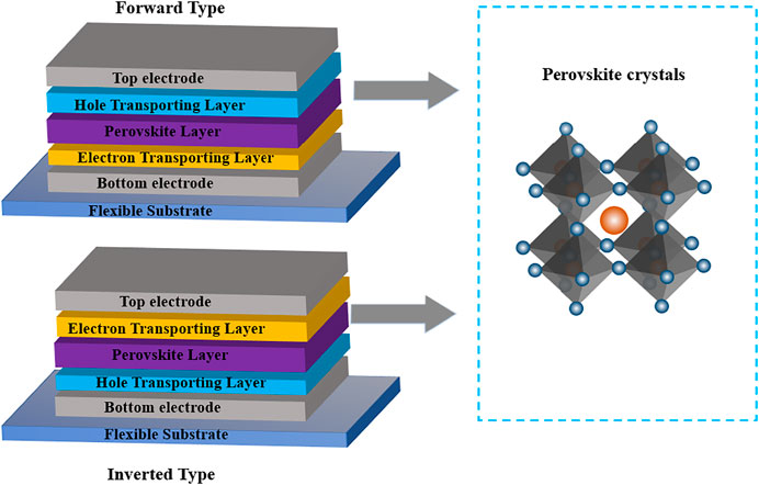
FIGURE 1. Two general device structures of perovskite solar cells.
It is well known that the fabrication process can directly influence the morphology of perovskite films, thus, it is worthwhile to summarize the various fabrication processes and the related film morphology (Elseman et al., 2020a; Elseman et al., 2020b). In this manuscript, we summarized the state-of-the-art fabrication processes and the effects on the perovskite film morphology. Furthermore, the overall device performance was also investigated, including efficiency, and stability. Finally, the prospect of the commercialization of perovskite photovoltaic applications is discussed based on the various fabrication process. The one-step and two-step sequence deposition methods are mostly investigated in lab experiments to achieve higher efficiency and to reveal the superiority of PSCs to improve the development and to gain more public attention. As the basic investigation of PSCs in the lab, the achievements could promote the development of the commercialization of PSCs.
Enormous efforts have been made during the past years and great achievements have been made in lab experiments. However, the efficiency of large-scale perovskite photovoltaic devices still falls far behind that of small size (<0.1 cm2) perovskite devices. It is necessary to summarize the recent achievements in large-scale fabrication processes to inspire further investigations. Therefore, we describe the perovskite solar cells in detail from the following aspects: 1) The basic investigation of the perovskite crystallization process, which includes one-step and two-step methods. 2) This part is the main content of the article. We discuss in detail the preparation methods and processes of large-area perovskites, such as vapor-assisted solution method, thermal vapor deposition, roll-to-roll fabrication techniques, inkjet printing, doctor-blade coating, slot-die coating, and spray-coating. These methods are the mainstream methods in the current research work, and we hope that the summary of these works will be helpful to the work of researchers in the perovskite field.
2 Deposition Methods
Fabrication strategies are divided into vapor assisted processing and wet chemistry processing. The wet chemistry processing methods are further categorized into one-step deposition techniques and two-step deposition techniques. Vapor assisted processing approaches additionally have exclusive processing strategies which include thermal vapor deposition (TVD) and vapor assisted solution procedure (VASP) (Barrows et al., 2014; Chen et al., 2014).In the following section, we will discuss the various fabrication process and the effects on the film morphology of the perovskite. More importantly, the related device performance is emphasized. We try to elaborate on the advantages and disadvantages of the various fabrication processes and evaluate the prospects for large-scale fabrication to realize the commercialization of PSCs.
2.1 The Basic Investigation of the Perovskite Crystallization Process
The final performance of the perovskite photovoltaic devices was almost totally dependant on the quality of the perovskite film. Thus, to obtain the high-quality perovskite film was highly desirable. In the following part of the text, we will discuss the crystallization process by illustrating the one- and two-step fabrication processes of perovskite photovoltaic devices.
2.1.1 One-Step Method
The one-step fabrication process has been widely studied and the investigation of the crystallization mechanism would inspire the large-scale fabrication process. The general crystallization process involves three steps: 1) the supersaturation of solution; 2) the formation of nuclei; 3) the growth of crystal (Jeon et al., 2015; Hsieh et al., 2018). With the assistance of the anti-solvent and the evaporation of the solvent, the solution is supersaturated, then the nucleation process starts, followed by the consumption of solute, and the start of the crystal growth. Previous investigations of the one-step fabrication process give the fundamental cognition of the crystallization process and it is worthwhile to be elaborated (Xiao et al., 2014a; Gardner et al., 2016; Hendriks et al., 2017).
The one-step method is commonly employed to deposit perovskite film because it is not only cheap in manufacturing but also additionally accessible in processing. Before spin coating, organic, and inorganic elements are mixed and dissolved in a polar solvent like dimethylsulfoxide (DMSO) or dimethylformamide (DMF) to form the precursor pigment. In some cases, the perovskite film will be evolved via spin coating of the pigment on a substrate, accompanied by post-annealing at 70–150°C (Roy et al., 2020). Due to the high boiling point and low vapor pressure and the annealing process, the solvent will evaporate and the perovskite structure could be formed. Gratzel and his group tested the results of the annealing temperature at the formation of CH3NH3PbI3 perovskite films by the one-step approach. They observed the coverage of the film increased against annealing temperature ranging 60–100°C (Pellet et al., 2014). The PSCs that annealed on the absorber layer at 100°C yield the highest efficiency (Yang et al., 2019). The first PSC was developed by Kojima and their group in 2009, and they investigated the optical properties of methylammonium lead iodide to make mixed halide or iodide only (Kojima et al., 2009). Organic halides (CH3NH3X) and lead halides (PbX2) had been dissolved in GBL, dimethylformamide DMSO or DMF in the nitrogen glove box to prepare a methylammonium lead halide (CH3NH3PbX3) solution as shown in the following equation.
The perovskite film was deposited via spin coating at the top of TiO2 layer as shown in Figure 2 (Ahmadian-Yazdi et al., 2016; Jamal et al., 2018).
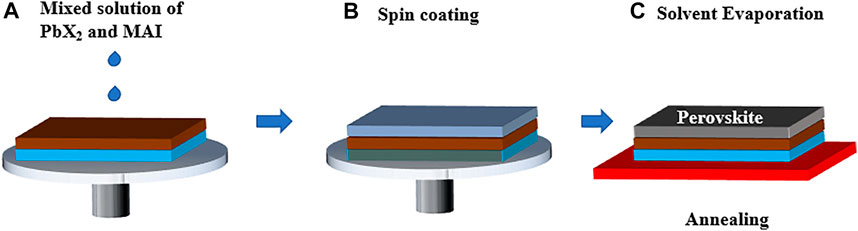
FIGURE 2. Schematic illustration of obtaining a perovskite layer by one step deposition method.
There is a drawback in the one-step method on a large area is better film coverage and uniform thickness of the layer. Anti-solvent precipitation is a well-known technique in chemistry to crystalize a material. The best thing is that this method is applied to the manufacturing of perovskite solar cells by using an anti-solvent dropping method. This approach became first reported through Jeon and his crew; they observed that using an anti-solvent in the fabrication of perovskite film produced first-class and dense films (Jeon et al., 2014). However, the anti-solvent preparation process should be conducted at right time and the volume should be precisely controlled. Besides, this anti-solvent step requires high proficiency. Furthermore, uncontrolled crystallization can form pin-holes which could damage the efficiency and stability of the devices (Zuo et al., 2018; Arain et al., 2019).
In addition to the anti-solvent method to accelerate the crystallization, the gas-assisted crystallization process was also investigated. Nie et al. (2015) developed the hot-casting process to accelerate the evaporation of the high-boiling solvent to render a high-quality perovskite film and a tunable perovskite morphology by tuning the temperature of the substrate. A vacuum-assisted solvent evaporation method was elaborated by Li et al. (2016). After the spin-coating process, the substrate was placed in the chamber under a vacuum environment to achieve the rapid evaporation of the solvent followed by the annealing process. Finally, a certified PCE of 19.6% was achieved under the active area over 1 cm2. However, the rapid evaporation process resulted in a faster nucleation rate thus decreasing the grain size. A deeper understanding of the crystallization mechanism should be sought to balance the solvent evaporation process and the crystallization process.
Though the one-step fabrication process delivers a feasible fabrication technique and high efficiency, the simple one-step spin-coating is not suitable for large-scale fabrication since a uniform and homogeneous perovskite film cannot be obtained. Luckily, the one-step fabrication process is popular in lab-scale investigations because of the simple preparation, and less requirement could deliver a good performance device which is beneficial for the future commercialization of PSCs.
2.1.2 Two-Step Method
To solve the uncontrollable film morphology fabricated by the one-step fabrication process, the two-step method was investigated. Usually, the one-step deposition method uses a combination of MAX and PbX2 that ends in the out-of-control precipitation of the perovskite, which leads to significant morphological variation that prevent the possibilities for commercial applications. Consequently, low-temperature two-step deposition methods become more advanced (Bi et al., 2013; Burschka et al., 2013). The two-step deposition approach is an excellent technique to clear up issues resulting from the dipping approach. In a two-step deposition approach, an inorganic solution is deposited on a substrate with the spin coating technique (Jiang et al., 2016). Consequently, the coated substrate is immersed into a second organic solution accompanied by annealing (Bi et al., 2014; Yang et al., 2017b). Take the well-studied perovskite MAPbI3 for instance: firstly, the PbI2 was spin-coated at the substrate; secondly, the resulting film was spin-coated with MAI solution or immersed in MAI solution. Followed by the annealing process, a high-quality perovskite film could be achieved. Furthermore, the deposition of methylammonium iodide (MAI) solution via spin coating over a PbI2 film has been employed followed by means of annealing as shown in Figure 3 (Im et al., 2014).
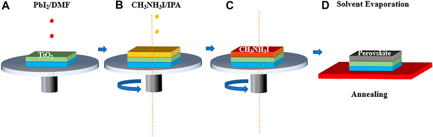
FIGURE 3. Schematic diagram of obtaining a perovskite layer by two-step spin coating method.
Though the sequence deposition process can deliver the full coverage film and large grain scale, however, the resultant film has a high surface roughness which will cause surface recombination loss (Yang et al., 2015; Yang et al., 2018b). Some researchers found that incomplete conversion of perovskite is a major issue in the two-step deposition method. The transformation speed of PbI2 to MAPbI3 is quite suitable after the film is immersed into the solution, due to the structural association of heavy metal halides that are inclined to engage with small molecules. Consequently, a compact perovskite layer is shaped on the pinnacle of PbI2 and the movement of MAI to the lowest layer is difficult, which becomes a cause of partial perovskite transformation (Coleman et al., 2011; Olaleru et al., 2020). Wu et al. solve this problem by introducing recently developed techniques which include solvent engineering and adding precursors to some additives like DMSO or H2O that can prevent the formation of a compact perovskite layer on the pinnacle of PbI2 (Wu et al., 2014; Wu et al., 2015; Olaleru et al., 2020). The strong coordination effect was observed between DMSO and Pb2+ ions to slow the crystallization of PbI2 in forming the amorphous PbI2 film, which could accelerate the complete conversion of the perovskite phase.
The one-and-a-half-step method combines the advantages of both the one-step and two-step deposition methods. In the first step, the preliminary perovskite phase was acquired via mesh assisted grid technology, and then the deposited perovskite grid was dipped into formamidinium iodide-isopropanol to transform it into the proper perovskite segment, which is termed the “half step.” The devices fabricated by using the one-and-a-half-step process display stronger performance than those fabricated through the one-step technique because of their advanced crystal quality, crystal size, absorbance, and stability (Rai et al., 2018). A novel fabrication process called the intramolecular exchange process (IEP) was investigated by Yang et al. The larger grain size and more homogeneous film deliver a PCE of over 20% (Yang et al., 2015).
Though the two-step sequence deposition process could produce a superior performance to the one-step fabrication process, this method still needs a more complicated fabrication process and annealing environment, and the second spin-coating process or the immersion step should be precisely controlled to get a high-quality perovskite film. High-performance perovskite devices are mostly based on the two-step sequence deposition process, and this method gets more attention in lab experiments. However, it is still not suitable for large-scale fabrication processing because of the complicated fabrication process accompanied by the waste of raw materials (Xiao et al., 2014b; Fan et al., 2017).
The one-step fabrication process and the two-step sequence deposition method are aimed to achieve superior performance of PSCs, and they usually do not account for the cost, furthermore, the traditional fabrication method is not suitable for the large-scale preparation. Thus, the above-mentioned methods are indicated as the groundbreaking investigation to be the foundation for commercial applications in the future of PSCs (Huang et al., 2016; Rahimnejad et al., 2016).
Due to the low formation energy of the perovskite structure, low-temperature large-scale fabrication processes could be realized according to investigations from lab experiments. In the following sections, we will discuss the large-scale fabrication processes and their advantages and disadvantages, respectively.
The one-step fabrication technique renders the simplest fabrication process and facilitates the understanding of the perovskite crystallization process. However, the uncontrollable crystallization process and relatively low efficiency limited its further investigation. The two-step fabrication process could deliver high efficiency, however, the issue of incomplete conversion of the precursor still needs further study.
2.2 Large-Scale Fabrication Process
As mentioned above, we have briefly summarized the fabrication process and the crystallization dynamics process which was beneficial and enlightened for the followed investigation. To realize the commercialization of the perovskite photovoltaic devices, the large-scale fabrication process was essential and unignorable. Great efforts have been made to explore the large-scale fabrication method. Herein, several advanced large-scale fabrication processes are summarized.
2.2.1 Vapor-Assisted Solution Method
Though the two-step sequence deposition fabrication process has made great achievements, most high-performance perovskite device is based on this method. However, the intrinsic drawbacks still limit the enhancement of performance for perovskite devices. The long-term conversion process of perovskite structure and the incomplete conversion of PbI2 would be harmful to the perovskite device. To solve the drawbacks of the two-step sequence deposition process (Zhu et al., 2018) the vapor-assisted deposition process was developed.
The vapor-assisted solution technique (Figure 4) is the further modification of the two-step deposition approach wherein MAI is deposited through a vapor deposition approach (Chen et al., 2014). This technique is based on the kinetic reactivity of MAI and the thermodynamic stability of perovskite throughout the growth process. The perovskite layer developed by this method offers excessive grain size, large crystal size, homogenous coverage, negligible surface roughness, and the full transformation of the perovskite (Hao et al., 2014). The fabricated devices generated an outstanding power conversion performance of 10.6% with excessive reproducibility showing a negligible deviation of 0.1%. Liu et al. fabricated the mixed halide perovskite film through the co-evaporation process by simultaneously evaporating the MAI and PbCl2, followed by the annealing process. The high-quality perovskite film was obtained with a uniform and full coverage. The sequential vaporization fabrication process was also investigated (Wang et al., 2014). Abbas et al. fabricated the PSCs by evaporating the PbI2 and MAI sequentially. The sequential evaporation process could render a more sufficient conversion of PbI2 (Zheng et al., 2020).
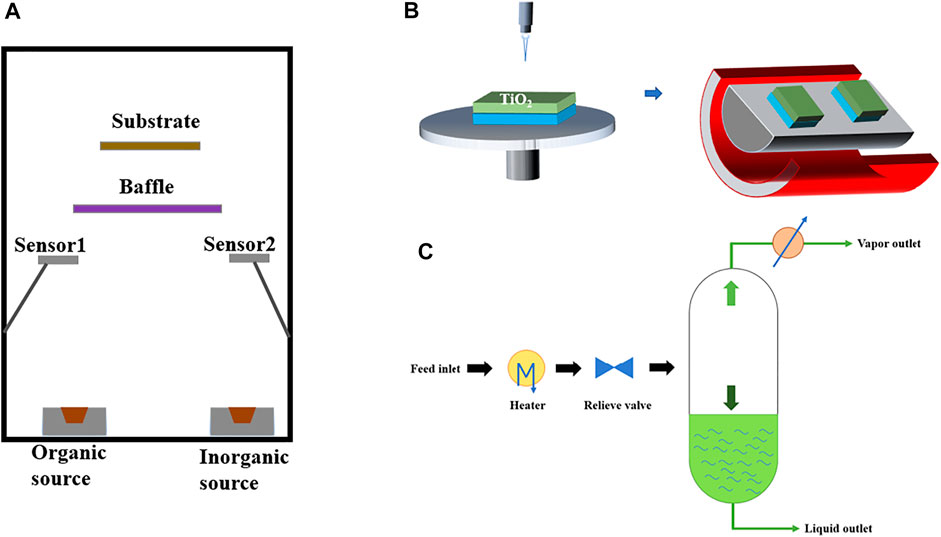
FIGURE 4. Classification of various vapor phase deposition techniques for PSCs.
Though the vapor-assisted solution method can relieve the disadvantages of the two-step sequence deposition process, this method is still not suitable for large-scale fabrication processes since this method still needs the spin-coating method to fabricate the first deposited film. The vapor-assisted solution technique can be divided into various detailed fabrication processes: 1) evaporate the material on the surface of the as-formed film; 2) deposit the film through the hot flow. The vapor-assisted solution method could also act as the post-treatment process to decrease the trap density and enhance the perovskite film quality.
2.2.2 Thermal Vapor Deposition
The thermal vapor deposition can also be divided into two versions: 1) the sequence deposition process; 2) the co-evaporation process.
The vapor deposition strategies are generally carried out by means of a high vacuum process. MAX and PbX2 are deposited consecutively or simultaneously at the TiO2 substrate through thermal evaporation. TVD for the perovskite absorber layers was reproduced by Liu et al. A MAPbI3 absorber was deposited via a dual-source evaporation system in a nitrogen-filled glove box. The primary advantage of the TVD is to supply a noticeably uniform layer and the coverage of the total surface area, but controlling the vapor phase reaction is decisive. On this approach, PbX2 and MAX were simultaneously evaporated from special sources at a precise molar ratio under an excessive vacuum. The vapor-deposited perovskite film is uniform, flat, and provides barely large crystal capabilities (Liu et al., 2013).
The co-evaporation process has drawbacks because the deposition rate is hard to control. The sequence evaporation method draws researchers’ attention, in which PbI2 was firstly evaporated, followed by the evaporation of MAI to fabricated the high-quality perovskite film.
Since the evaporation rate of organic material is hard to control, the thermal vapor deposition is very suitable for the fabrication of all-inorganic perovskite devices. Duan et al. fabricated the high-efficiency perovskite light-emitting devices by evaporating the CsPbBr3 (Chen et al., 2020). Wang et al. reached the record PCE of Cs2AgBiBr6 PSCs by the evaporation process. They claimed that the PSCs fabricated by thermal vapor deposition exhibited better performance than those fabricated by the solution spin-coating process (Igbari et al., 2019). Adachi et al. used the perovskite layer (MAPbCl3) fabricated by the thermal vapor deposition as the hole transport layer in organic light-emitting devices (OLED), and ultra-thick OLEDs could be achieved.
In the meantime, the thermal vapor deposition method is suitable for large-scale fabrication processes, which is inspired by the OLED fabrication process. The controllable thickness and the homogenous film quality render the possibility of the commercialization of perovskite applications.
2.2.3 Roll-To-Roll Fabrication Techniques
Roll-to-roll (R2R) is a promising solution processing strategy used for the production of PSC. The R2R fabrication technique has some basic necessities and enforces limits on the substrates and materials used: for high-speed production the substrate should be flexible, which requires low processing temperatures (<140°C) (Etgar et al., 2012). R2R includes exceptional coating techniques which are used to shape thin film on a substrate through the usage of rotating rolls as shown in Figure 5. These techniques could be used to manufacture perovskite solar cells on a flexible substrate.

FIGURE 5. Types of roll-to-roll fabrication techniques.
Essentially, a low crystallization energy barrier lets perovskite films be readily prepared by means of a low-temperature fabrication technique like R2R, which sets up a bridge between research and commercial applications. The slot-die coating approach is the appropriate approach for the deposition of HTL and ETL layers due to its highly uniform film deposition. R2R deposition is the continuous process of depositing layers on the substrate for making solar cells through the usage of various kinds of R2R compatible strategies. The excellent aspects of this form of deposition are that it is faster, exceptionally scalable, and cost-effective (Deng et al., 2015; Galagan et al., 2015).
2.2.4 Inkjet Printing
Inkjet Printing has precise control of patterns and ink consumption, and it is controlled by a computer program which provides a superior advantage in that the substrate has fewer limits. Inkjet printing can be used in flexible substrates with desired patterns, which represents the future development direction of flexible devices (Peng et al., 2017; Huang et al., 2019). Wei et al. firstly demonstrated the superiority of inkjet printing by fabricating perovskite devices using inkjet printing (Wei et al., 2014). However, the PbI2 layer was still fabricated by spin-coating. Further investigation was conducted by Song et al., who investigated the various parameters (e.g., substrate, ink character, precursor, and so on) which would affect the final perovskite films. By cautiously controlling the fabrication parameters (e.g., solvent, substrate) and combining with the MAI vapor post-treatment, the PCE of 17.74% could be achieved (Li et al., 2018a). This achievement inspired the following studies. The mechanism of the inkjet printing is shown in Figure 6.
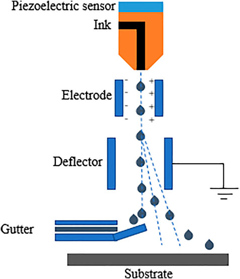
FIGURE 6. Schematic of perovskite film fabrication through inkjet printing.
The as-mentioned inkjet printing was based on the two-step fabrication process. In 2016, Quintilla and co-workers demonstrated a direct fabrication of perovskite devices by inkjet printing (Mathies et al., 2016). By combining the vacuum annealing process, they achieved a PCE of 11.3%. This work was a milestone for the commercialization of PSCs by the inkjet printing fabrication process.
The inkjet printing process has proved that scalable and reproducible devices could be achieved. However, the efficiency still falls far from the spin-coating process and the uniform film is hard to conduct. Unlike the perovskite devices fabricated in a glovebox, inkjet printing is mostly conducted in an atmospheric environment, there are so many parameters that would affect the quality of the obtained perovskite film, the detailed effects are still unclear, and the coffee ring effects still perplex the enhancement of perovskite device. However, by combining the investigations conducted on the spin-coating process and the deeper understanding crystallization process, the inkjet printing fabrication process still has the potential for large-scale fabrication. Furthermore, more efforts should be conducted in inkjet printing to solve the above-mentioned issues and to pursue the higher performance of perovskite devices fabricated by inkjet printing.
2.2.5 Doctor-Blade Coating
Doctor-blade coating is a scalable and simple fabrication process. Unlike inkjet printing, doctor-blade printing does not need expensive equipment and is easy to execute (Chen et al., 2009; Tian et al., 2012). The thickness of perovskite film can be easily controlled by the gap between blade and substrate, and the concentration of the solution can also affect the thickness of the obtained perovskite film. The perovskite precursor solution was purged on the substrate or flowed through the blade, followed by the swiping of the blade and the evaporation of the solution, and then the perovskite film can be obtained. In 2015, the doctor-blade coating was firstly demonstrated by Huang et al. However, the quality of the perovskite film was poor (Deng et al., 2015). The subsequent investigations explored the effects of substrate temperature on the crystallization process. The hot plate accelerated the nucleation process and the growth of the crystal. With MACl as the additive, an enlarged grain size could be achieved with a PCE of 19.3% (Li et al., 2018b).
The well-studied additive strategy in the spin-coating process can also be applied in doctor-blade coating. Inspired by the previous investigations, the adhesion between substrate and precursor solution was also investigated since the speed of the blade was so fast, to obtain a uniform and fully covered perovskite film (Bi et al., 2018). By adding a small amount of surfactants, L-α-phosphatidylcholine (LP), the wettability was enhanced between the substrate and the precursor solution. Through this strategy, a compact and uniform perovskite film could be obtained. The PCE of a large-scale perovskite device (33 cm2) reached 15.3% (Deng et al., 2018).
The doctor-blade coating process has the advantages of a low cost and an easy fabrication process. By utilizing the additive strategies of the well-established spin-coating process, accompanied with the preciously controlled fabrication parameters (e.g., substrate temperature, concentration of the solution, speed of blade), doctor-blade coating has a great potential for large-scale applications. The mechanism of the doctor-blade coating is shown in Figure 7.
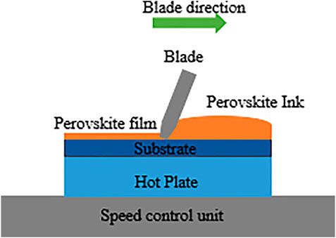
FIGURE 7. Schematic of perovskite film fabrication through doctor-blade coating.
2.2.6 Slot-Die Coating
Slot-die coating is similar to the doctor-blade coating, however, with the ink control system, a more precise control could be achieved, which means a better perovskite film morphology. The only drawback is that more perovskite precursor solution is needed (Krebs, 2009; Sandström et al., 2012). In 2015, Vak et al. first demonstrated that by combining the 3D print technique with slot-die coating to control the position of the coating tip. By using the two-step sequence deposition process through slot-die coating to fabricate the PbI2 film, followed by the vapor annealing, the high-quality perovskite film could be achieved, and the PCE of 11.96% could be achieved (Hwang et al., 2015). Byrkitt et al. (2018) fabricated the full slot-die coating device (except electrode), and this achievement points out the superiority of the slot-die coating. The additive strategy was also investigated, with the addition of NH4Cl as the additive, followed with the optimization of substrate temperature and airflow system, and a perovskite device with a PCE of 15.57% could be achieved (Jeong et al., 2019).
Compared with the doctor-blade coating, the slot-die coating provides a more precise control of the deposition process with the optimization of substrate temperature, the width between the blade and the substrate, and the speed of the fabrication process. The potential of slot-die coating can be emphasized. The mechanism of slot-die coating is shown in Figure 8.
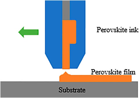
FIGURE 8. Schematic of perovskite film fabrication through slot-die coating.
2.2.7 Spray-Coating
Spray-coating has been widely investigated in organic photovoltaic devices and the technique has drawn researchers’ attention in the field of perovskite devices (Susanna et al., 2011; Lehraki et al., 2012; Jung et al., 2018). The basic process is as follows: 1) the perovskite precursor solution was dispersed to mist; 2) the mist was spread to the substrate by gas flow; 3) after the annealing process, the perovskite film was finished (Bishop et al., 2018). The first demonstration of the fabrication of perovskite film by spray-coating was conducted by Barrows et al. They investigated the various parameters (e.g., the temperature of the substrate, the annealing temperature, and time) which would affect the quality of the perovskite film. Finally, high-quality perovskite films could be produced and a PCE of 11% was achieved (Barrows et al., 2014). Further investigation was conducted by Ishihara et al. They studied the relationship between the surface tension and the quality of perovskite film. By using NMP and DMF as the solvent, a full-coverage perovskite film could be produced and a PCE of 14.2% was achieved (Ishihara et al., 2016). Inspired by the use of anti-solvent which was usually conducted in the one-step fabrication process, Yun et al. demonstrated a novel fabrication based on spray-coating, and the spray-antisolvent (SAS) technique was conducted. By using a metal mesh as the electrode, a large-scale (16 cm2) PSCs model was demonstrated with a PCE of 12.1% (Kim et al., 2017). The mechanism of spray-coating was shown in Figure 9.
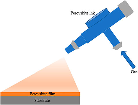
FIGURE 9. Schematic of perovskite film fabrication through spray-coating.
Spray-coating shows great potential in the future large-scale application of perovskite devices, however, the deeper mechanisms should be studied such as the properties of the substrate and perovskite precursor solution, the speed of spray-coating, and the annealing process. More effects should be conducted on spray-coating to realize cost-effective perovskite devices. Table 1 shows the important parameters of perovskite solar cells through the various fabrication process.
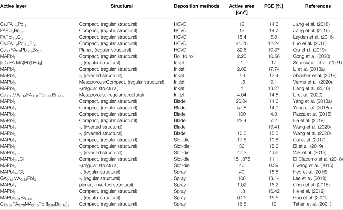
TABLE 1. The perovskite solar cells through the various fabrication process.
3 Conclusion
In this manuscript, we summarized the various fabrication process of perovskite devices, including the well-established one-step and two-step deposition processes which can render high-performance PSCs. One- and two-step spin-coating processes were the precursory investigation to explore their properties for future commercial applications. Though the record PCE was exhilarating, the spin-coating process was not suitable for commercialization. The vapor-based deposition process could render the high-quality film and accurate thickness. However, vapor-based fabrication needs more energy consumption. As for the roll-to-roll fabrication process, it is suitable for flexible perovskite photovoltaic devices. The precise control of thickness and the film morphology is its bottleneck. The doctor-blade coating, slot-die coating, and spray coating also have the same problems as the roll-to-roll fabrication process. Thus, we consider the inkjet printing process as the most promising technique for further application in large-scale perovskite devices. Inkjet printing could precisely control the droplet size and the trajectory, and has the virtues of a precise patterning ability and material-conserving characteristics. This fabrication process is suitable for various substrates. The large-scale fabrication process for commercialization is elaborated, and the advantages and disadvantages are discussed. Though great achievements have been made for large-scale fabrication processes during the past years, there are still some parameters that should be optimized:
1) The treatment of the substrate should be emphasized since the substrate temperature, the wettability of the substrate, and the cleanliness of the substrate can affect the obtained perovskite film.
2) The importance of the perovskite precursor solution should be elaborated since the crystallization process is heavily dependent on the solution composition, concentration, and types of solvent.
3) The fabrication process of large-scale devices should be optimized. The fabrication parameters should be widely investigated and carefully adjusted to obtain high-quality perovskite film.
4) To expand the large-scale fabrication process to various functional layers to shorten the preparation time of the entire device.
We predict that by combining the well-established one-step and two-step fabrication processes with the optimization of the novel large-scale fabrication process, the forecast of large scale applications is hopeful. Except for the high efficiency and the large-scale fabrication processes, the powerful encapsulation technique should be on the agenda to prolong the lifetime of the entire device.
Finally, with the efforts all we made, the dawn of the commercial perovskite devices will surely come.
Author Contributions
ZC proposes writing ideas and completes the writing of the main part of the article and PH participates in the writing part. DW draws the pictures, CC designed the main frame of the article. MM helped the author investigate the data. YL provided writing advice, YD made critical comments and revisions to the article.
Funding
This study was supported by the National Natural Science Foundation of China (Grant Nos. 61974054 and 61675088), the International Science & Technology Cooperation Program of Jilin (Gra-nt No. 20190701023GH), the Scientific and Technological Developing Scheme of Jilin Province (Grants Nos. 20200401045GX), and the Project of Science and Technology Development Plan of Jilin Province (Grant No. 20190302011G).
Conflict of Interest
The authors declare that the research was conducted in the absence of any commercial or financial relationships that could be construed as a potential conflict of interest.
Publisher’s Note
All claims expressed in this article are solely those of the authors and do not necessarily represent those of their affiliated organizations, or those of the publisher, the editors and the reviewers. Any product that may be evaluated in this article, or claim that may be made by its manufacturer, is not guaranteed or endorsed by the publisher.
References
Abzieher, T., Moghadamzadeh, S., Schackmar, F., Eggers, H., Sutterlüti, F., Farooq, A., et al. (2019). Electron‐Beam‐Evaporated Nickel Oxide Hole Transport Layers for Perovskite‐Based Photovoltaics. Adv. Energ. Mater. 9, 1802995. doi:10.1002/aenm.201802995
Ahmadian-Yazdi, M. R., Zabihi, F., Habibi, M., and Eslamian, M. (2016). Effects of Process Parameters on the Characteristics of Mixed-Halide Perovskite Solar Cells Fabricated by One-step and Two-step Sequential Coating. Nanoscale Res. Lett. 11, 408. doi:10.1186/s11671-016-1601-8
Arain, Z., Liu, C., Yang, Y., Mateen, M., Ren, Y., Ding, Y., et al. (2019). Elucidating the Dynamics of Solvent Engineering for Perovskite Solar Cells. Sci. China Mater. 62, 161–172. doi:10.1007/s40843-018-9336-1
Bansal, S., and Aryal, P. (2016). “Evaluation of New Materials for Electron and Hole Transport Layers in Perovskite-Based Solar Cells through SCAPS-1D Simulations,” in IEEE 43rd Photovoltaic Specialists Conference (PVSC), Portland, OR, 5–10 June, 2016. doi:10.1109/pvsc.2016.7749702
Barrows, A. T., Pearson, A. J., Kwak, C. K., Dunbar, A. D. F., Buckley, A. R., and Lidzey, D. G. (2014). Efficient Planar Heterojunction Mixed-Halide Perovskite Solar Cells Deposited via spray-deposition. Energy Environ. Sci. 7, 2944–2950. doi:10.1039/c4ee01546k
Bi, D., Moon, S.-J., Häggman, L., Boschloo, G., Yang, L., Johansson, E. M. J., et al. (2013). Using a Two-step Deposition Technique to Prepare Perovskite (CH3NH3PbI3) for Thin Film Solar Cells Based on ZrO2 and TiO2 Mesostructures. RSC Adv. 3, 18762. doi:10.1039/c3ra43228a
Bi, D., El-Zohry, A. M., Hagfeldt, A., and Boschloo, G. (2014). Improved Morphology Control Using a Modified Two-step Method for Efficient Perovskite Solar Cells. ACS Appl. Mater. Inter. 6, 18751–18757. doi:10.1021/am504320h
Bi, Z., Rodríguez-Martínez, X., Aranda, C., Pascual-San-José, E., Goñi, A. R., Campoy-Quiles, M., et al. (2018). Defect Tolerant Perovskite Solar Cells from Blade Coated Non-toxic Solvents. J. Mater. Chem. A. 6, 19085–19093. doi:10.1039/c8ta06771f
Bi, E., Tang, W., Chen, H., Wang, Y., Barbaud, J., Wu, T., et al. (2019). Efficient Perovskite Solar Cell Modules with High Stability Enabled by Iodide Diffusion Barriers. Joule 3, 2748–2760. doi:10.1016/j.joule.2019.07.030
Bishop, J. E., Routledge, T. J., and Lidzey, D. G. (2018). Advances in spray-cast Perovskite Solar Cells. J. Phys. Chem. Lett. 9, 1977–1984. doi:10.1021/acs.jpclett.8b00311
Burkitt, D., Searle, J., and Watson, T. (2018). Perovskite Solar Cells in N-I-P Structure with Four Slot-Die-Coated Layers. R. Soc. Open Sci. 5, 172158. doi:10.1098/rsos.172158
Burschka, J., Pellet, N., Moon, S.-J., Humphry-Baker, R., Gao, P., Nazeeruddin, M. K., et al. (2013). Sequential Deposition as a Route to High-Performance Perovskite-Sensitized Solar Cells. Nature 499, 316–319. doi:10.1038/nature12340
Cai, L., Liang, L., Wu, J., Ding, B., Gao, L., and Fan, B. (2017). Large Area Perovskite Solar Cell Module. J. Semicond. 38, 014006. doi:10.1088/1674-4926/38/1/014006
Chen, D., Huang, F., Cheng, Y.-B., and Caruso, R. A. (2009). Mesoporous Anatase TiO2Beads with High Surface Areas and Controllable Pore Sizes: A Superior Candidate for High-Performance Dye-Sensitized Solar Cells. Adv. Mater. 21, 2206–2210. doi:10.1002/adma.200802603
Chen, Q., Zhou, H., Hong, Z., Luo, S., Duan, H.-S., Wang, H.-H., et al. (2014). Planar Heterojunction Perovskite Solar Cells via Vapor-Assisted Solution Process. J. Am. Chem. Soc. 136, 622–625. doi:10.1021/ja411509g
Chen, W., Wu, Y., Yue, Y., Liu, J., Zhang, W., Yang, X., et al. (2015). Efficient and Stable Large-Area Perovskite Solar Cells with Inorganic Charge Extraction Layers. Science 350, 944–948. doi:10.1126/science.aad1015
Chen, C., Han, T.-H., Tan, S., Xue, J., Zhao, Y., Liu, Y., et al. (2020). Efficient Flexible Inorganic Perovskite Light-Emitting Diodes Fabricated with CsPbBr3 Emitters Prepared via Low-Temperature In Situ Dynamic Thermal Crystallization. Nano Lett. 20, 4673. doi:10.1021/acs.nanolett.0c01550
Coleman, J. N., Lotya, M., O’Neill, A., Bergin, S. D., King, P. J., Khan, U., et al. (2011). Two-dimensional Nanosheets Produced by Liquid Exfoliation of Layered Materials. Science 331, 568–571. doi:10.1126/science.1194975
De Wolf, S., Holovsky, J., Moon, S.-J., Löper, P., Niesen, B., Ledinsky, M., et al. (2014). Organometallic Halide Perovskites: Sharp Optical Absorption Edge and its Relation to Photovoltaic Performance. J. Phys. Chem. Lett. 5, 1035–1039. doi:10.1021/jz500279b
Deng, Y., Peng, E., Shao, Y., Xiao, Z., Dong, Q., and Huang, J. (2015). Scalable Fabrication of Efficient Organolead Trihalide Perovskite Solar Cells with Doctor-Bladed Active Layers. Energ. Environ. Sci. 8, 1544–1550. doi:10.1039/c4ee03907f
Deng, Y., Zheng, X., Bai, Y., Wang, Q., Zhao, J., and Huang, J. (2018). Surfactant-controlled Ink Drying Enables High-Speed Deposition of Perovskite Films for Efficient Photovoltaic Modules. Nat. Energ. 3, 560–566. doi:10.1038/s41560-018-0153-9
Di Giacomo, F., Shanmugam, S., Fledderus, H., Bruijnaers, B. J., Verhees, W. J. H., Dorenkamper, M. S., et al. (2018). Up-scalable sheet-to-sheet production of high efficiency perovskite module and solar cells on 6-in. substrate using slot die coating. Solar Energ. Mater. Solar Cell 181, 53–59. doi:10.1016/j.solmat.2017.11.010
Elseman, A. M., Sharmoukh, W., Sajid, S., Cui, P., Ji, J., Dou, S., et al. (2019). Superior Stability and Efficiency over 20% Perovskite Solar Cells Achieved by a Novel Molecularly Engineered Rutin-AgNPs/Thiophene Copolymer. Adv. Sci. (Weinh) 5, 1800568. doi:10.1002/advs.201800568
Elseman, A. M., Zaki, A. H., Shalan, A. E., Rashad, M. M., and Song, Q. L. (2020). TiO2 Nanotubes: An Advanced Electron Transport Material for Enhancing the Efficiency and Stability of Perovskite Solar Cells. Ind. Eng. Chem. Res. 59, 18549–18557. doi:10.1021/acs.iecr.0c03415
Elseman, A. M., Xu, C., Yao, Y., Elisabeth, M., Niu, L., Malavasi, L., et al. (2020). Electron Transport Materials: Evolution and Case Study for High‐Efficiency Perovskite Solar Cells. Sol. RRL 4, 2000136. doi:10.1002/solr.202000136
Etgar, L., Gao, P., Xue, Z., Peng, Q., Chandiran, A. K., Liu, B., et al. (2012). Mesoscopic CH3NH3PbI3/TiO2 Heterojunction Solar Cells. J. Am. Chem. Soc. 134, 17396–17399. doi:10.1021/ja307789s
Fan, L., Ding, Y., Luo, J., Shi, B., Yao, X., Wei, C., et al. (2017). Elucidating the Role of Chlorine in Perovskite Solar Cells. J. Mater. Chem. A. 5, 7423–7432. doi:10.1039/c7ta00973a
Galagan, Y., Fledderus, H., Gorter, H., 't Mannetje, H. H., Shanmugam, S., Mandamparambil, R., et al. (2015). Roll-to-Roll Slot-Die Coated Organic Photovoltaic (OPV) Modules with High Geometrical Fill Factors. Energ. Techn. 3, 834–842. doi:10.1002/ente.201500150
Gardner, K. L., Tait, J. G., Merckx, T., Qiu, W., Paetzold, U. W., Kootstra, L., et al. (2016). Nonhazardous Solvent Systems for Processing Perovskite Photovoltaics. Adv. Energ. Mater. 6, 1600386. doi:10.1002/aenm.201600386
Gong, C., Tong, S., Huang, K., Li, H., Huang, H., Zhang, J., et al. (2020). Flexible Planar Heterojunction Perovskite Solar Cells Fabricated via Sequential Roll‐to‐Roll Microgravure Printing and Slot‐Die Coating Deposition. Sol. RRL 4, 1900204. doi:10.1002/solr.201900204
Guo, A. Z., Chou, L. H., Yang, S. H., Wang, D., Wang, X. F., Osaka, I., et al. (2021). Multi‐Channel Pumped Ultrasonic Spray‐Coating for High‐Throughput and Scalable Mixed Halide Perovskite Solar Cells. Adv. Mater. Inter. 8, 2001509. doi:10.1002/admi.202001509
Han, Y., Meyer, S., Dkhissi, Y., Weber, K., Pringle, J. M., Bach, U., et al. (2015). Degradation Observations of Encapsulated Planar CH3NH3PbI3 Perovskite Solar Cells at High Temperatures and Humidity. J. Mater. Chem. A. 3, 8139–8147. doi:10.1039/c5ta00358j
Hao, F., Stoumpos, C. C., Liu, Z., Chang, R. P., and Kanatzidis, M. G. (2014). Controllable Perovskite Crystallization at a Gas-Solid Interface for Hole Conductor-free Solar Cells with Steady Power Conversion Efficiency over 10%. J. Am. Chem. Soc. 136, 16411–16419. doi:10.1021/ja509245x
He, S., Qiu, L., Son, D.-Y., Liu, Z., Juarez-Perez, E. J., Ono, L. K., et al. (2019). Carbon-Based Electrode Engineering Boosts the Efficiency of All Low-Temperature-Processed Perovskite Solar Cells. ACS Energ. Lett. 4, 2032–2039. doi:10.1021/acsenergylett.9b01294
Hendriks, K. H., van Franeker, J. J., Bruijnaers, B. J., Anta, J. A., Wienk, M. M., and Janssen, R. A. J. (2017). 2-Methoxyethanol as a New Solvent for Processing Methylammonium lead Halide Perovskite Solar Cells. J. Mater. Chem. A. 5, 2346–2354. doi:10.1039/c6ta09125c
Heo, J. H., Lee, M. H., Jang, M. H., and Im, S. H. (2016). Highly Efficient CH3NH3PbI3−xClx Mixed Halide Perovskite Solar Cells Prepared by Re-dissolution and crystal Grain Growth via spray Coating. J. Mater. Chem. A. 4, 17636–17642. doi:10.1039/c6ta06718b
Hsieh, H.-C., Yu, J., Rwei, S.-P., Lin, K.-F., Shih, Y.-C., and Wang, L. (2018). Ultra-compact Titanium Oxide Prepared by Ultrasonic spray Pyrolysis Method for Planar Heterojunction Perovskite Hybrid Solar Cells. Thin Solid Films 659, 41–47. doi:10.1016/j.tsf.2018.05.002
Huang, H., Shi, J., Zhu, L., Li, D., Luo, Y., and Meng, Q. (2016). Two-step Ultrasonic spray Deposition of CH3NH3PbI3 for Efficient and Large-Area Perovskite Solar Cell. Nano Energy 27, 352–358. doi:10.1016/j.nanoen.2016.07.026
Huang, F., Li, M., Siffalovic, P., Cao, G., and Tian, J. (2019). From Scalable Solution Fabrication of Perovskite Films towards Commercialization of Solar Cells. Energ. Environ. Sci. 12, 518–549. doi:10.1039/c8ee03025a
Hwang, K., Jung, Y.-S., Heo, Y.-J., Scholes, F. H., Watkins, S. E., Subbiah, J., et al. (2015). Toward Large Scale Roll-To-Roll Production of Fully Printed Perovskite Solar Cells. Adv. Mater. 27, 1241–1247. doi:10.1002/adma.201404598
Igbari, F., Wang, R., Wang, Z.-K., Ma, X.-J., Wang, Q., Wang, K.-L., et al. (2019). Composition Stoichiometry of Cs2AgBiBr6 Films for Highly Efficient lead-free Perovskite Solar Cells. Nano Lett. 19, 2066–2073. doi:10.1021/acs.nanolett.9b00238
Im, J.-H., Jang, I.-H., Pellet, N., Grätzel, M., and Park, N.-G. (2014). Growth of CH3NH3PbI3 Cuboids with Controlled Size for High-Efficiency Perovskite Solar Cells. Nat. Nanotech. 9, 927–932. doi:10.1038/nnano.2014.181
Ishihara, H., Sarang, S., Chen, Y.-C., Lin, O., Phummirat, P., Thung, L., et al. (2016). Nature Inspiring Processing Route toward High Throughput Production of Perovskite Photovoltaics. J. Mater. Chem. A. 4, 6989–6997. doi:10.1039/c5ta09992g
Jamal, M. S., Bashar, M. S., Hasan, A. K. M., Almutairi, Z. A., Alharbi, H. F., Alharthi, N. H., et al. (2018). Fabrication Techniques and Morphological Analysis of Perovskite Absorber Layer for High-Efficiency Perovskite Solar Cell: A Review. Renew. Sustain. Energ. Rev. 98, 469–488. doi:10.1016/j.rser.2018.09.016
Jeon, N. J., Noh, J. H., Kim, Y. C., Yang, W. S., Ryu, S., and Seok, S. I. (2014). Solvent Engineering for High-Performance Inorganic-Organic Hybrid Perovskite Solar Cells. Nat. Mater 13, 897–903. doi:10.1038/nmat4014
Jeon, N. J., Noh, J. H., Yang, W. S., Kim, Y. C., Ryu, S., Seo, J., et al. (2015). Compositional Engineering of Perovskite Materials for High-Performance Solar Cells. Nature 517, 476–480. doi:10.1038/nature14133
Jeong, D.-N., Lee, D.-K., Seo, S., Lim, S. Y., Zhang, Y., Shin, H., et al. (2019). Perovskite Cluster-Containing Solution for Scalable D-Bar Coating toward High-Throughput Perovskite Solar Cells. ACS Energ. Lett. 4, 1189–1195. doi:10.1021/acsenergylett.9b00042
Jiang, Q., Zhang, L., Wang, H., Yang, X., Meng, J., Liu, H., et al. (2016). Enhanced Electron Extraction Using SnO2 for High-Efficiency Planar-Structure HC(NH2)2PbI3-based Perovskite Solar Cells. Nat. Energ. 2, 16177. doi:10.1038/nenergy.2016.177
Jiang, Y., Leyden, M. R., Qiu, L., Wang, S., Ono, L. K., Wu, Z., et al. (2018). Combination of Hybrid CVD and Cation Exchange for Upscaling Cs-Substituted Mixed Cation Perovskite Solar Cells with High Efficiency and Stability. Adv. Funct. Mater. 28, 1703835. doi:10.1002/adfm.201703835
Jiang, Y., Remeika, M., Hu, Z., Juarez‐Perez, E. J., Qiu, L., Liu, Z., et al. (2019). Negligible‐Pb‐Waste and Upscalable Perovskite Deposition Technology for High‐Operational‐Stability Perovskite Solar Modules. Adv. Energ. Mater. 9, 1803047. doi:10.1002/aenm.201803047
Jung, Y.-S., Hwang, K., Heo, Y.-J., Kim, J.-E., Vak, D., and Kim, D.-Y. (2018). Progress in Scalable Coating and Roll-To-Roll Compatible Printing Processes of Perovskite Solar Cells toward Realization of Commercialization. Adv. Opt. Mater. 6, 1701182. doi:10.1002/adom.201701182
Kajal, P., Ghosh, K., and Powar, S. (2018). “Manufacturing Techniques of Perovskite Solar Cells,” in Applications of Solar Energy (Singapore: Springer), 341–364. Energy, Environment, and Sustainability. doi:10.1007/978-981-10-7206-2_16
Kim, J., Yun, J. S., Cho, Y., Lee, D. S., Wilkinson, B., Soufiani, A. M., et al. (2017). Overcoming the Challenges of Large-Area High-Efficiency Perovskite Solar Cells. ACS Energ. Lett. 2, 1978–1984. doi:10.1021/acsenergylett.7b00573
Kojima, A., Teshima, K., Shirai, Y., and Miyasaka, T. (2009). Organometal Halide Perovskites as Visible-Light Sensitizers for Photovoltaic Cells. J. Am. Chem. Soc. 131, 6050–6051. doi:10.1021/ja809598r
kour, N., Mehra, R., and Chandni, (2018). Efficient Design of Perovskite Solar Cell Using Mixed Halide and Copper Oxide. Chin. Phys. B 27, 018801. doi:10.1088/1674-1056/27/1/018801
Krebs, F. C. (2009). Polymer Solar Cell Modules Prepared Using Roll-To-Roll Methods: Knife-Over-Edge Coating, Slot-Die Coating and Screen Printing. Solar Energ. Mater. Solar Cell 93, 465–475. doi:10.1016/j.solmat.2008.12.012
Lee, D.-K., Jeong, D.-N., Ahn, T. K., and Park, N.-G. (2019). Precursor Engineering for a Large-Area Perovskite Solar Cell with > 19% Efficiency. Acs Energ. Lett. 4, 2393–2401. doi:10.1021/acsenergylett.9b01735
Lehraki, N., Aida, M. S., Abed, S., Attaf, N., Attaf, A., and Poulain, M. (2012). ZnO Thin Films Deposition by spray Pyrolysis: Influence of Precursor Solution Properties. Curr. Appl. Phys. 12, 1283–1287. doi:10.1016/j.cap.2012.03.012
Leyden, M. R., Jiang, Y., and Qi, Y. (2016). Chemical Vapor Deposition Grown Formamidinium Perovskite Solar Modules with High Steady State Power and thermal Stability. J. Mater. Chem. A. 4, 13125–13132. doi:10.1039/c6ta04267h
Li, X., Tschumi, M., Han, H., Babkair, S. S., Alzubaydi, R. A., Ansari, A. A., et al. (2015). Outdoor Performance and Stability under Elevated Temperatures and Long-Term Light Soaking of Triple-Layer Mesoporous Perovskite Photovoltaics. Energ. Techn. 3, 551–555. doi:10.1002/ente.201500045
Li, X., Bi, D., Yi, C., Décoppet, J.-D., Luo, J., Zakeeruddin, S. M., et al. (2016). A Vacuum Flash-Assisted Solution Process for High-Efficiency Large-Area Perovskite Solar Cells. Science 353, 58–62. doi:10.1126/science.aaf8060
Li, P., Liang, C., Bao, B., Li, Y., Hu, X., Wang, Y., et al. (2018). Inkjet Manipulated Homogeneous Large Size Perovskite Grains for Efficient and Large-Area Perovskite Solar Cells. Nano Energy 46, 203–211. doi:10.1016/j.nanoen.2018.01.049
Li, J., Munir, R., Fan, Y., Niu, T., Liu, Y., Zhong, Y., et al. (2018). Phase Transition Control for High-Performance Blade-Coated Perovskite Solar Cells. Joule 2, 1313–1330. doi:10.1016/j.joule.2018.04.011
Li, Z., Li, P., Chen, G., Cheng, Y., Pi, X., Yu, X., et al. (2020). Ink Engineering of Inkjet Printing Perovskite. ACS Appl. Mater. Inter. 12, 39082–39091. doi:10.1021/acsami.0c09485
Liang, C., Li, P., Gu, H., Zhang, Y., Li, F., Song, Y., et al. (2018). One‐Step Inkjet Printed Perovskite in Air for Efficient Light Harvesting. Sol. RRL 2, 1700217. doi:10.1002/solr.201700217
Liu, M., Johnston, M. B., and Snaith, H. J. (2013). Efficient Planar Heterojunction Perovskite Solar Cells by Vapour Deposition. Nature 501, 395–398. doi:10.1038/nature12509
Luo, L., Zhang, Y., Chai, N., Deng, X., Zhong, J., Huang, F., et al. (2018). Large-area Perovskite Solar Cells with CsxFA1 xPbI3 yBry Thin Films Deposited by a Vapor-Solid Reaction Method. J. Mater. Chem. A. 6, 21143–21148. doi:10.1039/c8ta06557h
Mathies, F., Abzieher, T., Hochstuhl, A., Glaser, K., Colsmann, A., Paetzold, U. W., et al. (2016). Multipass Inkjet Printed Planar Methylammonium lead Iodide Perovskite Solar Cells. J. Mater. Chem. A. 4, 19207–19213. doi:10.1039/c6ta07972e
Nie, W., Tsai, H., Asadpour, R., Blancon, J.-C., Neukirch, A. J., Gupta, G., et al. (2015). High-efficiency Solution-Processed Perovskite Solar Cells with Millimeter-Scale Grains. Science 347, 522–525. doi:10.1126/science.aaa0472
Olaleru, S. A., Kirui, J. K., Wamwangi, D., Roro, K. T., and Mwakikunga, B. (2020). Perovskite Solar Cells: The New Epoch in Photovoltaics. Solar Energy 196, 295–309. doi:10.1016/j.solener.2019.12.025
Pascoe, A. R., Meyer, S., Huang, W., Li, W., Benesperi, I., Duffy, N. W., et al. (2016). Enhancing the Optoelectronic Performance of Perovskite Solar Cells via a Textured CH3NH3PbI3Morphology. Adv. Funct. Mater. 26, 1278–1285. doi:10.1002/adfm.201504190
Pellet, N., Gao, P., Gregori, G., Yang, T.-Y., Nazeeruddin, M. K., Maier, J., et al. (2014). Mixed-organic-cation Perovskite Photovoltaics for Enhanced Solar-Light Harvesting. Angew. Chem. Int. Ed. 53, 3151–3157. doi:10.1002/anie.201309361
Peng, X., Yuan, J., Shen, S., Gao, M., Chesman, A. S. R., Yin, H., et al. (2017). Perovskite and Organic Solar Cells Fabricated by Inkjet Printing: Progress and Prospects. Adv. Funct. Mater. 27, 1703704. doi:10.1002/adfm.201703704
Qiu, L., He, S., Jiang, Y., Son, D.-Y., Ono, L. K., Liu, Z., et al. (2019). Hybrid Chemical Vapor Deposition Enables Scalable and Stable Cs-FA Mixed Cation Perovskite Solar Modules with a Designated Area of 91.8 Cm(2) Approaching 10% Efficiency. J. Mater. Chem. A 7, 6920–6929. doi:10.1039/c9ta00239a
Rahimnejad, S., Kovalenko, A., Forés, S. M., Aranda, C., and Guerrero, A. (2016). Coordination Chemistry Dictates the Structural Defects in lead Halide Perovskites. ChemPhysChem 17, 2795–2798. doi:10.1002/cphc.201600575
Rai, M., Rahmany, S., Lim, S. S., Magdassi, S., Wong, L. H., and Etgar, L. (2018). Hot Dipping post Treatment for Improved Efficiency in Micro Patterned Semi-transparent Perovskite Solar Cells. J. Mater. Chem. A. 6, 23787–23796. doi:10.1039/c8ta09340g
Razza, S., Di Giacomo, F., Matteocci, F., Cinà, L., Palma, A. L., Casaluci, S., et al. (2015). Perovskite Solar Cells and Large Area Modules (100 Cm 2 ) Based on an Air Flow-Assisted PbI 2 Blade Coating Deposition Process. J. Power Sourc. 277, 286–291. doi:10.1016/j.jpowsour.2014.12.008
Roy, P., Kumar Sinha, N., Tiwari, S., and Khare, A. (2020). A Review on Perovskite Solar Cells: Evolution of Architecture, Fabrication Techniques, Commercialization Issues and Status. Solar Energy 198, 665–688. doi:10.1016/j.solener.2020.01.080
Sajid, S., Elseman, A. M., Wei, D., Ji, J., Dou, S., Huang, H., et al. (2019). Corrigendum to "NiO@Carbon Spheres: A Promising Composite Electrode for Scalable Fabrication of Planar Perovskite Solar Cells at Low Cost" [Nano Energy, 55 (2019) 470-476]. Nano Energy 58, 94–95. doi:10.1016/j.nanoen.2019.01.016
Sandström, A., Dam, H. F., Krebs, F. C., and Edman, L. (2012). Ambient Fabrication of Flexible and Large-Area Organic Light-Emitting Devices Using Slot-Die Coating. Nat. Commun. 3, 1002–1005. doi:10.1038/ncomms2002
Schackmar, F., Eggers, H., Frericks, M., Richards, B. S., Lemmer, U., Hernandez‐Sosa, G., et al. (2021). Perovskite Solar Cells with All‐Inkjet‐Printed Absorber and Charge Transport Layers. Adv. Mater. Technol. 6, 2000271. doi:10.1002/admt.202000271
Selim, M. S., Elseman, A. M., and Hao, Z. (2020). ZnO Nanorods: An Advanced Cathode Buffer Layer for Inverted Perovskite Solar Cells. ACS Appl. Energ. Mater. 3, 11781–11791. doi:10.1021/acsaem.0c01945
Snaith, H. J. (2018). Present Status and Future Prospects of Perovskite Photovoltaics. Nat. Mater 17, 372–376. doi:10.1038/s41563-018-0071-z
Susanna, G., Salamandra, L., Brown, T. M., Di Carlo, A., Brunetti, F., and Reale, A. (2011). Airbrush spray-coating of Polymer Bulk-Heterojunction Solar Cells. Solar Energ. Mater. Solar Cell 95, 1775–1778. doi:10.1016/j.solmat.2011.01.047
Taheri, B., De Rossi, F., Lucarelli, G., Castriotta, L. A., Di Carlo, A., Brown, T. M., et al. (2021). Laser-Scribing Optimization for Sprayed SnO2-Based Perovskite Solar Modules on Flexible Plastic Substrates. ACS Appl. Energ. Mater. 4, 4507–4518. doi:10.1021/acsaem.1c00140
Tian, J., Gao, R., Zhang, Q., Zhang, S., Li, Y., Lan, J., et al. (2012). Enhanced Performance of CdS/CdSe Quantum Dot Cosensitized Solar Cells via Homogeneous Distribution of Quantum Dots in TiO2 Film. J. Phys. Chem. C 116, 18655–18662. doi:10.1021/jp3058838
Vak, D., Hwang, K., Faulks, A., Jung, Y.-S., Clark, N., Kim, D.-Y., et al. (2015). 3D Printer Based Slot-Die Coater as a Lab-To-Fab Translation Tool for Solution-Processed Solar Cells. Adv. Energ. Mater. 5, 1401539. doi:10.1002/aenm.201401539
Verma, A., Martineau, D., Abdolhosseinzadeh, S., Heier, J., and Nüesch, F. (2020). Inkjet Printed Mesoscopic Perovskite Solar Cells with Custom Design Capability. Mater. Adv. 1, 153–160. doi:10.1039/d0ma00077a
Wang, Q., Shao, Y., Dong, Q., Xiao, Z., Yuan, Y., and Huang, J. (2014). Large Fill-Factor Bilayer Iodine Perovskite Solar Cells Fabricated by a Low-Temperature Solution-Process. Energ. Environ. Sci. 7, 2359–2365. doi:10.1039/c4ee00233d
Wang, Y., Li, M., Zhou, X., Li, P., Hu, X., and Song, Y. (2018). High Efficient Perovskite Whispering-Gallery Solar Cells. Nano Energy 51, 556–562. doi:10.1016/j.nanoen.2018.06.085
Wang, Z., Zeng, L., Zhang, C., Lu, Y., Qiu, S., Wang, C., et al. (2020). Rational Interface Design and Morphology Control for Blade-Coating Efficient Flexible Perovskite Solar Cells with a Record Fill Factor of 81%. Adv. Funct. Mater. 30(32), 2001240. doi:10.1002/adfm.202001240
Wei, Z., Chen, H., Yan, K., and Yang, S. (2014). Inkjet Printing and Instant Chemical Transformation of a CH3NH3PbI3/nanocarbon Electrode and Interface for Planar Perovskite Solar Cells. Angew. Chem. Int. Ed. 53, 13239–13243. doi:10.1002/anie.201408638
Wu, Y., Islam, A., Yang, X., Qin, C., Liu, J., Zhang, K., et al. (2014). Retarding the Crystallization of PbI2for Highly Reproducible Planar-Structured Perovskite Solar Cells via Sequential Deposition. Energ. Environ. Sci. 7, 2934–2938. doi:10.1039/c4ee01624f
Wu, C.-G., Chiang, C.-H., Tseng, Z.-L., Nazeeruddin, M. K., Hagfeldt, A., and Grätzel, M. (2015). High Efficiency Stable Inverted Perovskite Solar Cells without Current Hysteresis. Energ. Environ. Sci. 8, 2725–2733. doi:10.1039/c5ee00645g
Xiao, M., Huang, F., Huang, W., Dkhissi, Y., Zhu, Y., Etheridge, J., et al. (2014). A Fast Deposition-Crystallization Procedure for Highly Efficient Lead Iodide Perovskite Thin-Film Solar Cells. Angew. Chem. Int. Ed. 53, 9898–9903. doi:10.1002/anie.201405334
Xiao, Z., Bi, C., Shao, Y., Dong, Q., Wang, Q., Yuan, Y., et al. (2014). Efficient, High Yield Perovskite Photovoltaic Devices Grown by Interdiffusion of Solution-Processed Precursor Stacking Layers. Energ. Environ. Sci. 7, 2619–2623. doi:10.1039/c4ee01138d
Xu, C. Y., Hu, W., Wang, G., Niu, L., Elseman, A. M., Liao, L., et al. (2020). Coordinated Optical Matching of a Texture Interface Made from Demixing Blended Polymers for High-Performance Inverted Perovskite Solar Cells. Acs Nano 14, 196–203. doi:10.1021/acsnano.9b07594
Yang, W. S., Noh, J. H., Jeon, N. J., Kim, Y. C., Ryu, S., Seo, J., et al. (2015). High-performance Photovoltaic Perovskite Layers Fabricated through Intramolecular Exchange. Science 348, 1234–1237. doi:10.1126/science.aaa9272
Yang, M., Li, Z., Reese, M. O., Reid, O. G., Kim, D. H., Siol, S., et al. (2017). Perovskite Ink with Wide Processing Window for Scalable High-Efficiency Solar Cells. Nat. Energ. 2, 17038. doi:10.1038/nenergy.2017.38
Yang, W. S., Park, B.-W., Jung, E. H., Jeon, N. J., Kim, Y. C., Lee, D. U., et al. (2017). Iodide Management in formamidinium-lead-halide-based Perovskite Layers for Efficient Solar Cells. Science 356, 1376–1379. doi:10.1126/science.aan2301
Yang, M., Kim, D. H., Klein, T. R., Li, Z., Reese, M. O., Tremolet de Villers, B. J., et al. (2018). Highly Efficient Perovskite Solar Modules by Scalable Fabrication and Interconnection Optimization. ACS Energ. Lett. 3, 322–328. doi:10.1021/acsenergylett.7b01221
Yang, D., Yang, R., Wang, K., Wu, C., Zhu, X., Feng, J., et al. (2018). High Efficiency Planar-type Perovskite Solar Cells with Negligible Hysteresis Using EDTA-Complexed SnO2. Nat. Commun. 9, 3239–3311. doi:10.1038/s41467-018-05760-x
Yang, D., Yang, R., Priya, S., and Liu, S. (2019). Recent Advances in Flexible Perovskite Solar Cells: Fabrication and Applications. Angew. Chem. Int. Ed. 58, 4466–4483. doi:10.1002/anie.201809781
Zheng, X., Hou, Y., Bao, C., Yin, J., Yuan, F., Huang, Z., et al. (2020). Managing Grains and Interfaces via Ligand Anchoring Enables 22.3%-efficiency Inverted Perovskite Solar Cells. Nat. Energ. 5, 131–140. doi:10.1038/s41560-019-0538-4
Zhu, X., Xu, Z., Zuo, S., Feng, J., Wang, Z., Zhang, X., et al. (2018). Vapor-fumigation for Record Efficiency Two-Dimensional Perovskite Solar Cells with superior Stability. Energ. Environ. Sci. 11, 3349–3357. doi:10.1039/c8ee02284d
Keywords: perovskite, fabrication, solar cell, large scale, roll to roll
Citation: Chen Z, He P, Wu D, Chen C, Mujahid M, Li Y and Duan Y (2021) Processing and Preparation Method for High-Quality Opto-Electronic Perovskite Film. Front. Mater. 8:723169. doi: 10.3389/fmats.2021.723169
Received: 10 June 2021; Accepted: 04 October 2021;
Published: 26 October 2021.
Edited by:
Assa Aravindh Sasikala Devi, University of Oulu, FinlandReviewed by:
Sai Santosh Kumar Raavi, Indian Institute of Technology Hyderabad, IndiaAhmed Mourtada Elseman, Central Metallurgical Research and Development Institute (CMRDI), Egypt
Copyright © 2021 Chen, He, Wu, Chen, Mujahid, Li and Duan. This is an open-access article distributed under the terms of the Creative Commons Attribution License (CC BY). The use, distribution or reproduction in other forums is permitted, provided the original author(s) and the copyright owner(s) are credited and that the original publication in this journal is cited, in accordance with accepted academic practice. No use, distribution or reproduction is permitted which does not comply with these terms.
*Correspondence: Ye Li, bGl5ZUBjdXN0LmVkdS5jbg==; Yu Duan, ZHVhbnl1QGpsdS5lZHUuY24=
†These authors have contributed equally to this work