 Nilay Maji
 Subhasis Shit
 T. K. Nath
95% of researchers rate our articles as excellent or good
Learn more about the work of our research integrity team to safeguard the quality of each article we publish.
Find out more
ORIGINAL RESEARCH article
Front. Mater. , 01 October 2021
Sec. Thin Solid Films
Volume 8 - 2021 | https://doi.org/10.3389/fmats.2021.721031
This article is part of the Research Topic Thin Films and Fine Powders of Ferrites View all 6 articles
In this article, the fabrication of a Ni0.65Zn0.35Fe2O4/MgO/p-Si heterostructure device has been optimized using the pulsed laser deposition (PLD) technique, and a detailed investigation of its structural, electrical, and magnetic features has been performed experimentally. The electronic and magneto-transport characteristics have been explored in the temperature range of 100–300 K. The current-voltage (I-V) characteristics of the heterojunction have been recorded, which displayed an excellent rectifying magnetic tunnel diode-like behavior throughout that temperature regime. The application of an external magnetic field parallel to the plane of the NZFO film causes the current (I) across the junction to decrease, clearly indicating positive junction magnetoresistance (JMR) of the heterostructure. The root of displaying positive magnetoresistance in our heterojunction has been well justified using the standard spin injection model. The electrical injection of spin-polarized carriers and its accumulation and detection in a p-Si channel have been demonstrated using the NZFO/MgO tunnel contact using a three-terminal (3-T) Hanle device. The parameters such as spin lifetime (99 ps), spin diffusion length (276 nm), and spin polarization (0.44) have been estimated from the Hanle curve detected in our heterostructure at room temperature, making the Ni0.65Zn0.35Fe2O4/MgO/p-Si device a very favorable promising junction structure in the field of spintronics for several device appliances in the future.
With the precipitous advancement of novel devices miniaturizing technology, magnetic structures are being moved toward the nanoscale dimensions for promising applications in spintronics, memory, and other multi-functional devices (McCurrie, 1994; Sugimoto, 1999; Wolf et al., 2001; Parkin et al., 2008; Cullity and Graham, 2011; Zabel and Farle, 2012; Sharma et al., 2018). Among the several magnetic materials, the most remarkable and notable materials are strongly correlated spinel oxides of the AB2O4 structure, specifically the spinel ferrites possessing the general formula AFe2O4 (McCurrie, 1994; Cullity and Graham, 2011; Valenzuela, 2012; Thakur et al., 2017). Numerous spinel ferrites have already been reported to exhibit strong magnetic properties along with high Curie temperature; high resistivity; good chemical, structural, and thermal stabilities; high magnetostriction; and high dielectric permittivity (Sugimoto, 1999; Valenzuela, 2012). These ferrites also provide a nonzero magnetic moment along with spin-dependent band gaps (Sugimoto, 1999; Valenzuela, 2012; Thakur et al., 2017; Emori et al., 2018). Of late, nickel–zinc ferrites have become the most favorable ferromagnetic materials, owning to low dielectric losses, high saturation magnetization, high magnetostriction, low coercive field, high dielectric constant with magnetic transition temperature well above 300 K (Sugimoto, 1999; Valenzuela, 2012; Dionne and West, 1987; Srinivasan et al., 1988; Pradhan et al., 2014). This ferromagnetic material has already been used in various applications such as magnetic storage systems, gas sensors, catalysts, magnetic fluids, photo-magnetic materials, magnetic resonance imaging, site-specific drug delivery, and microwave devices (Raikher et al., 2004; Cunningham et al., 2005; Rana et al., 2005; Yoon et al., 2005; Chu et al., 2007). Now what stays behind to be focused is spin injection from the nickel–zinc ferrite magnetic film into a semiconductor. So, keeping the exceptional electro-magnetic properties of this nickel–ferrite material in mind, we have deposited a thin film of nickel–zinc ferrite on a semiconductor substrate to investigate whether this material can be a good choice for spin injection. Here, we have selected the composition Ni0.65Zn0.35Fe2O4 (NZFO) because the exceptional features such as the highest value of saturation magnetization in the entire Ni-Zn series, significant magnetostriction (λ100 = −24 × 10−6, λ111 = −13.2 × 10⁻⁶), and high value of magnetic transition temperature above 600 K (Dionne and West, 1987; Srinivasan et al., 1988; Pradhan et al., 2014) have been displayed by this optimized composition of Ni and Zn.
In this work, fabrication of a Ni0.65Zn0.35Fe2O4 (NZFO)/MgO/p-Si–optimized heterostructure has been reported, and its electro-magnetic transport properties have been investigated in detail. The current-voltage (I-V) characteristics of the heterojunction have been studied explicitly without and with the application of an external magnetic field up to 6 T in the temperature regime of 100–300 K. The heterostructure displays a rectifying magnetic diode–like feature at room temperature as well as at low temperatures. The magnetic field-dependent junction magnetoresistance characteristics of our heterostructure have been studied at different isothermal conditions. The robust value of positive JMR (∼870%) estimated at 100 K makes our device a promising candidate for magnetic field sensors, which can be used to read data in hard disk drives, biosensors, microelectromechanical systems (MEMS) (Reig et al., 2013). The standard spin injection model has been employed in order to explain the source of getting a positive value of JMR in our heterojunction. Such kind of giant JMR detected in a magnetic/semiconductor heterostructure at lower temperatures has already been reported (Qu et al., 2007; Maji et al., 2018).
The experimental details (device fabrication, characterization, and measurement setup) have been provided in the Supporting Information.
In order to investigate the crystal structure and the crystalline quality of our PLD-grown and annealed thin films of NZFO, the high-resolution X-ray diffraction (HR-XRD) scan was executed employing a Philips PANalytical X’Pert PRO diffractometer with Cu Kα radiation (λ ̴ 1.542 Å). Typical symmetric θ–2θ scans were recorded between 20° and 60° with a step size of 0.03° at a scanning rate of 1° per minute.
Not a single impurity peak has been detected within the resolution of our measurement. The x-ray diffraction pattern, shown in Figure 1A, reveals well-defined Bragg peaks [JCPDS card No. 08-0234], showing a good polycrystalline nature with reasonably good crystallinity. All the Bragg peaks are attributed to a cubic spinel structure (Kumbhar et al., 2014). Further evaluation of our XRD data with the help of the well-established Bragg’s law delivers the value of the lattice parameter (a) of our NZFO thin film as a = 8.326 ± 0.001 Å.
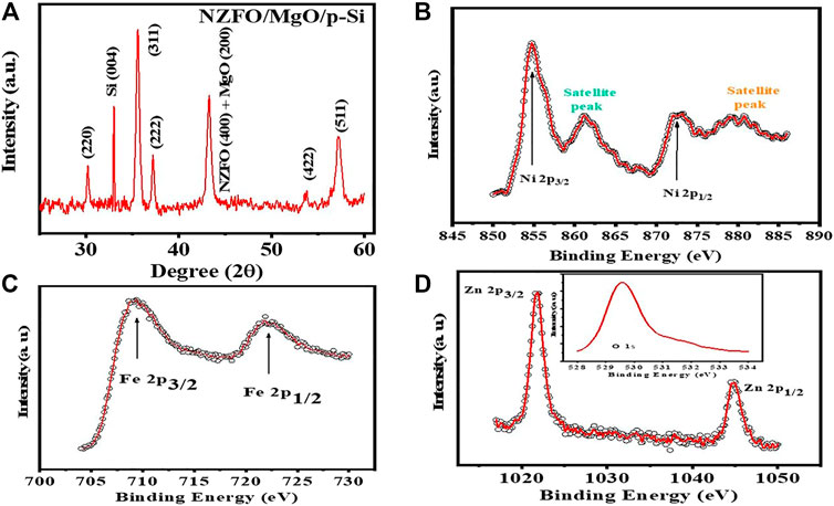
FIGURE 1. (A) High-resolution X-ray diffraction scan of the NZFO film deposited on the MgO/p-Si heterostructure. (B–D) XPS spectra of the synthesized nickel–zinc ferrite film for Ni 2p, Fe 2p, and Zn 2p core levels, respectively. The inset of (D) represents the O 1s core level.
The X-ray photoelectron spectroscopy (XPS) analysis has been done in order to get an idea about the overall chemical composition and chemical valence state of the ions in nickel–zinc ferrite thin films. The XPS spectra of the synthesized nickel–zinc ferrite film for Ni 2p, Fe 2p, and Zn 2p core levels are shown in Figure 1B–D, respectively. The film is found to be composed of Ni, Fe, and Zn with corresponding binding energies (BE in eV) of 854.6 (Ni 2p3/2), 872.5 (Ni 2p1/2), 710.40 (Fe 2p3/2), 723.96 (Fe 2p1/2), 1,020.83 eV (Zn 2p3/2), and 1,045.40 (Zn 2p3/2), respectively, and the values shown here belong to Ni2+, Fe3+, and Zn2+. The O 1s spectra achieved from the XPS study normally display the major peak with a binding energy value of 529.61 eV (inset of Figure 1D). These values tally very well with the values reported in the literature (Li et al., 2020). The outputs of the XPS study are consistent with the HR-XRD results, proving the growth of single-phase nickel–zinc ferrite thin films rather than a mixed impure phase.
Figure 2A displays the cross-sectional high-resolution transmission electron microscopy (HR-TEM) image of the NZFO/MgO/p-Si heterostructure. The HR-TEM image undoubtedly discloses the growth of a polycrystalline NZFO film, and the film is detached well from the p-Si wafer via the intermediate MgO layer (∼2–3 nm) with sharp interfaces. This thin layer of MgO has a significant role in spin injection into a semiconductor (p-Si) as it removes the spin impedance mismatch problem between the NZFO film and p-Si wafer. Moreover, the spin filtering effect of a very thin MgO tunnel barrier layer was also reported earlier in magnetic tunnel junctions (Butler, 2008).
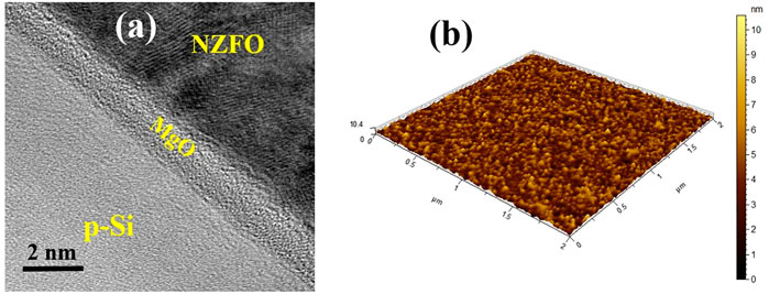
FIGURE 2. (A) High-resolution TEM image (crosssectional view) of the NZFO/MgO/p-Si heterojunction. (B) 3-D AFM image of the NZFO thin film.
Atomic force microscopy (AFM) has been employed in tapping mode to record the surface topography of the as-grown NZFO thin film. Figure 2B shows the 3-D AFM image of the as-grown magnetite thin film in the scan area (2 μm × 2 μm). The average rms surface roughness of the film has been found to be 0.9 nm, clearly revealing that the film is grown uniformly on the surface of MgO/p-Si device with full coverage. Depositing a smooth film is vital for spintronic device applications, because if the surface of the film is not smooth enough, then the inhomogeneous local magnetic field can hinder the accumulation of spin-polarized carriers in the semiconductor channel (Dash et al., 2011).
To explore the magnetic property of our PLD-grown NZFO film, the magnetization (M) of the thin film has been recorded as a function of the magnetic field applied parallel to the film plane at different isothermal conditions using a vibrating sample magnetometer (VSM). This magnetic study discloses that the film is ferrimagnetically soft along the in-plane direction of the thin film. Figure 3 displays the magnetic field-dependent magnetization curve of the NZFO thin film recorded at different isothermal conditions. As temperature decreases, the observed saturation magnetization value (∼364.64 emu/c.c.) at 300 K increases at 5 K (∼489 emu/c.c.).
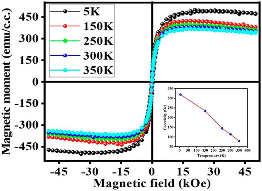
FIGURE 3. Magnetic field (H)-dependent isothermal (5, 150, 250, 300, and 350 K) magnetization (M) behavior of the NZFO film. The inset shows the variation of coercivity with temperature.
In the Ni–Zn mixed spinel ferrite system (Ni1-xZnxFe2O4), Ni2+ and Zn2+ ions are occupied in octahedral (B) and tetrahedral (A) sites in the lattice, respectively, whereas Fe3+ ions are distributed among both the sites. It is reported that the increase of x (Zn2+) in the tetrahedral side causes the transfer of some Fe3+ ions from the A site to the B site, which in turn increases the magnetization in the octahedral site. As a result, they exhibit higher saturation magnetization (Ms) with improved ferrimagnetic properties.
The magnetization measurement validates that the NZFO thin film displays improved ferrimagnetic hysteresis behavior compared to that of the NFO film (Maji et al., 2021) even at room temperature. The room temperature saturation magnetization (Ms) of the NFO film (Maji et al., 2021) is found to be 74 emu/c.c., whereas for the NZFO film, the value of Ms becomes 364.64 emu/c.c. This enhanced ferrimagnetism makes NZFO a promising applicant as an excellent spin injector at room temperature.
The coercivity is found to be 114.15 Oe at room temperature, and it validates the soft ferrimagnetic behavior of our NZFO film. The coercive field is also very sensitive to the applied temperature of our magnetic NZFO film. The inset of Figure 3 displays the variation of coercivity with temperature. As the temperature decreases, more numbers of magnetic spins are going to freeze in the anisotropic directions. This spin-freezing effect, which can arise due to exchange coupling between the core and surface spins, is dominant at low temperatures. As a result, the value of the coercive field increases with decreasing temperature.
In order to study the electrical transport characteristics of the NZFO/MgO/p-Si heterojunction, the current-voltage (I-V) data were recorded with biasing voltage from +6 V to −6 V at different isothermal conditions in the temperature regime of 100–300 K.
The schematic diagram of recording of the I-V data is shown in Figure 4A. Pure indium (In) metal has been used to make the contacts on the p-Si substrate and NZFO film. The current (I) vs. voltage (V) characteristics of the p-Si/In and In/NZFO contacts show linear (ohmic) behavior throughout the temperature range of 100–300 K. However, the I-V characteristics of the heterostructure display a nonlinear behavior throughout the temperature regime (Figure 4B). Since both the contacts are ohmic in nature, we can say that this nonlinearity arises because of the formation of heterojunction.
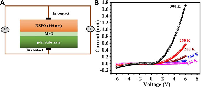
FIGURE 4. (A) Schematic device geometry for recording I-V data for the NZFO/MgO/p-Si heterojunction. (B) I-V curve of the heterojunction measured in the temperature regime of 100–300 K.
The current-voltage (I-V) characteristics of the heterojunction, which display an excellent rectifying magnetic diode-like behavior throughout the entire temperature regime, can be best fitted using the modified diode equation expressed by
where I0, η, and Rs are the reverse saturation current, ideality factor, and junction series resistance, respectively. The fitted plots are shown in Figure 5, and the obtained parameters are summarized in Table 1. In general, the value of η is ∼1 for an ideal metal/semiconductor junction having thermionic emission, and η ∼2 indicates that the process is mainly a recombination degeneration and diffusion process. Table 1 depicts that at all temperatures, the obtained values of ideality factors are much greater than 2, evidently suggesting that the conduction process is predominantly influenced by the tunneling mechanism across the heterojunction. Higher the value of the ideality factor, higher is the strength of tunneling (Maji et al., 2018).
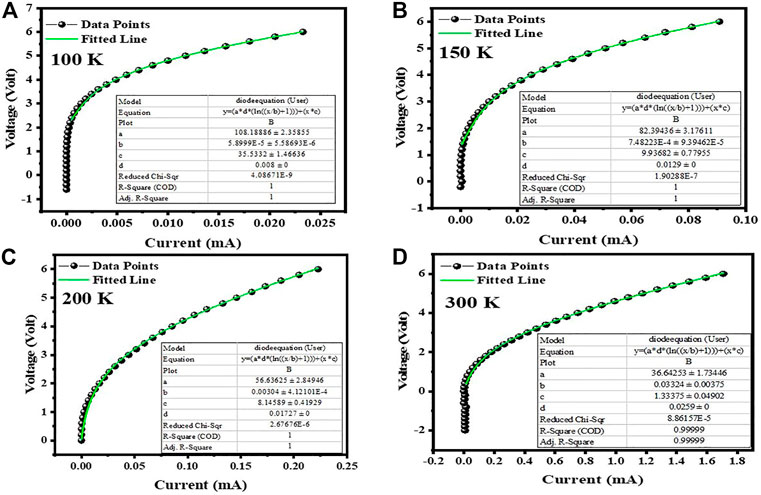
FIGURE 5. Best-fitted I-V characteristics of the NZFO/MgO/p-Si heterojunction at (A) 100 K, (B) 150 K, (C) 200 K, and (D) 300 K.
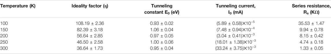
TABLE 1. Temperature dependence of extracted parameters (after fitting the I-V curve with diode equation) such as ideality factor, tunneling constant, tunneling current, and series resistance of the NZFO/MgO/p-Si heterostructure.
As the conduction process is predominantly governed by quantum mechanical tunneling, we express I0 as the tunneling saturation current and E0 (∼ηκBΤ) as the tunneling constant (Maji et al., 2018).
The ideality factor and tunneling saturation current have been observed to be strongly temperature-dependent (Figure 6A, B). Here, the tunneling saturation current increases and η decreases with increasing temperature. As the temperature upsurges, more number of carriers will gain sufficient energy to cross the barrier height. Therefore, the tunneling saturation current will rise with increasing temperature. As the tunneling current rises with temperature, the value of series resistance falls with rising temperature (Figure 6C). The tunneling constant, which is also termed as the voltage factor, essentially does not depend on temperature (Figure 6D) for the current transport dominated by quantum mechanical tunneling.
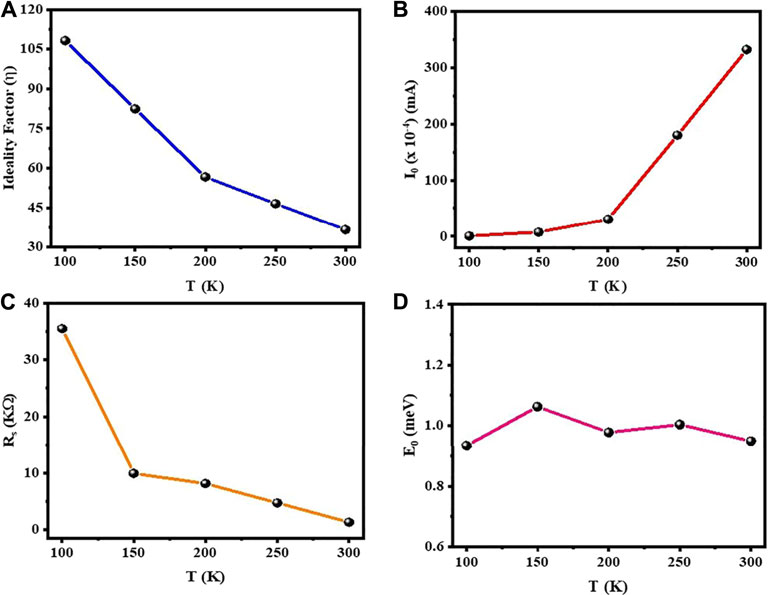
FIGURE 6. Variation of the (A) ideality factor, (B) tunneling saturation current, (C) series resistance, and (D) tunneling constant of the NZFO/MgO/p-Si heterojunction with temperature.
The typical conductance versus voltage (dI/dV-V) characteristics in the temperature regime of 100–300 K for the NZFO/MgO/p-Si heterostructure has been displayed in Figure 7. The lowest value of conductance has been observed at a relatively low dc bias voltage which indicates that the height of the potential barrier at the NZFO/MgO interface, at low bias voltage, is nearly equal to that at the p-Si/MgO interface. A significant increase in conductance has clearly been spotted as the bias voltage V is increased to a higher value. This is the typical signature of quantum mechanical tunneling with applied voltage for any heterostructure (Maji et al., 2018). Hence, it is crucial to quest for the probable tunneling mechanism across the junction in our heterostructure. The observed field stimulated emission can be discussed in terms of Fowler–Nordheim (FN) tunneling (Chakraborty et al., 2007), the Poole-Frenkel effect (Vincent et al., 1979; Buchwald and Johnson, 1988; Ganichev et al., 2000), phonon-assisted tunneling (Tsybeskov et al., 1999), and a combination of both phenomena (Vincent et al., 1979). FN tunneling is the process by which electrons tunnel through a barrier in the existence of a high electric field. FN tunneling current through a triangular barrier at a high electric field is provided by Eq. 2:
where A = q3/8πhϕB and Z = [8π(2mFN)1/2 ϕB3/2]/3qh (Tsybeskov et al., 1999). Here, q is the electronic charge, ϕB and mFN are the tunneling barrier height and effective mass of electron, respectively, and V is the applied voltage. The high-field FN tunneling should not be a function of temperature. But our studied curve of (ln (IFN/V2)) versus 1/V strongly depends on the temperature at this field range (Figure 8A), and hence, it can be concluded that FN tunneling most likely does not play any role here.
FIGURE 7. Plot of conductance versus voltage of the NZFO/MgO/p-Si heterostructure recorded in the temperature regime of 100–300 K.
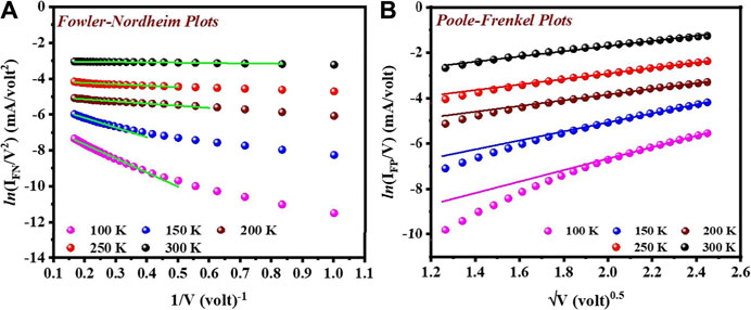
FIGURE 8. (A) Fowler–Nordheim plots of the NZFO/MgO/p-Si heterostructure at B = 0 T. (B) Poole–Frenkel plots for the same heterostructure in the absence of magnetic field.
The Poole–Frenkel effect depicts the enhancement in the rate of thermal emission of carriers in the presence of an exterior electric field because of the decreasing in the barrier related to their Coulomb potential. The Poole–Frenkel emission current density is given by
Vincent et al. (1979), where ϕB and Ɛs are the barrier height and relative dielectric permittivity, respectively (Vincent et al., 1979; Buchwald and Johnson, 1988).
From Figure 8B, we can notice that at high electric fields, the plots of ln (IFP/V) vs.
The I–V data for NZFO/MgO/p-Si heterojunction without and with 6 T applied magnetic field have been recorded at different isothermal conditions. The magnetic field is applied parallel to the plane of the NZFO film. The inset of Figure 9A displays the schematic setup for measuring the magneto-transport property of our heterostructure. Figures 9A,B display magnetic field-dependent I-V characteristics at 100 and 300 K, respectively. From Figures 9A,B, we can see that the junction current is noticeably cut down at a low temperature (100 K) as well as at room temperature by the application of an external magnetic field in forward bias. However, there is no significant change observed in the junction current in reverse bias condition. Since the junction current (NZFO/MgO/p-Si) is reduced by applying the external magnetic field, we can conclude that the system exhibits positive junction magnetoresistance (JMR) behavior.
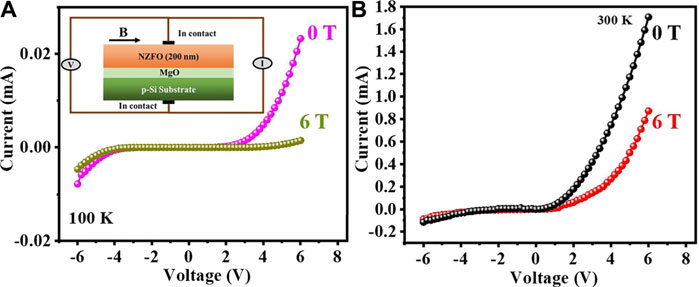
FIGURE 9. I–V characteristics of the heterostructure at (A) 100 K and (B) 300 K in the absence and presence of applied 6 T magnetic field. The inset of Figure 9A displays the schematic setup for measuring the magneto-transport property of our heterostructure.
The junction magnetoresistance behavior of our heterostructure has been studied at two different temperatures (100 and 300 K) for a constant forward dc bias voltage of 3 V in presence of an in-plane external magnetic field (B). The change in current across the junction (NZFO/MgO/p-Si) with the applied magnetic field has been recorded in the CPP (current perpendicular to plane direction) geometry. Figure 10A depicts the percentage change in JMR of the heterojunction with the variation of applied magnetic field up to 6 T at two different temperatures. The value of positive junction magnetoresistance at 100 K is nearly 870%, whereas at room temperature, it decreases (∼228%) significantly.
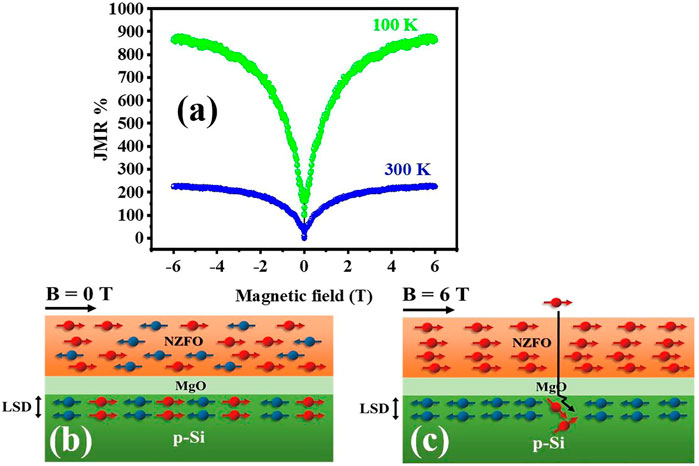
FIGURE 10. (A) Percentage change of JMR of the heterojunction with the change in magnetic field up to 6 T at two different isothermal conditions (100 and 300 K). (B,C) Schematic diagrams of the suggested spin injection model of the NZFO/p-Si heterostructure which explains the source of positive JMR in our heterojunction.
The JMR is well described by the formula
Several research groups have reported earlier about the formation of positive junction magnetoresistance in such magnetic/semiconductor heterostructures (Maji et al., 2018). The root of exhibiting positive magnetoresistance by our heterojunction can be well understood by the standard spin injection model. According to this model, the structure is composed of three layers: 1) the upper layer is the magnetic NZFO film, 2) the middle layer is the thin MgO layer, 3) the bottom layer is a thin layer (composed of the spins of the injected carriers from the ferrimagnetic NZFO film) in the vicinity of the interface between the ultrathin oxide barrier (MgO) and p-Si wafer. This case is very similar to a magnetic tunnel junction (MTJ), where the insulating nonmagnetic oxide layer acts as a tunnel barrier between the domains in the magnetic NZFO thin film and p-type silicon. When a saturation magnetic field is applied parallel to the NZFO film plane, the film tends to achieve its saturation magnetization value by changing the domain orientation along the field direction. We expect that the magnetic moment of the spins piled up at the bottom layer is lined up along the antiparallel direction of the NZFO film. Under these circumstances, the injected carrier encounters spin-dependent scattering due to the antiparallel orientation of spin layers in the heterostructure, and it possesses positive JMR (Figure 10B). We can also see that the JMR value decreases as the temperature increases because, due to phonon vibrations, the frozen carriers in the semiconductor gain adequate thermal energy to overcome the magnetic energy accountable for forming the induced antiparallel domains in the semiconductor channel. Under these circumstances, the induced domains tend to take a random orientation. This is the main reason for decreasing the JMR value with increasing temperature.
In order to inject as well as to detect spins in semiconductors, the three-terminal Hanle structure (Maji and Nath, 2019; Maji and Nath, 2020) has been constructed with the help of the vacuum masking method. The 3-T tunnel contacts (“a”, “b”, and “c”), made on the Hanle device having the dimension of 200 μm2 × 300 μm2, are well separated from each other by a distance of 300 μm (≫ spin diffusion length).
A constant current has been sent through the channel “a” to “b” with the help of a constant current source and inserted a voltmeter in the path of “a” to “c” (left inset of Figure 11A). After that an external magnetic field (B) is applied parallel to the magnetic NZFO film. Figure 11A shows the change in ΔV (spin accumulation in p-Si) as a function of an applied longitudinal magnetic field at a constant bias current of 5 μA at 300 K. We can notice that as the applied magnetic field becomes more intense, the ΔV [= V(B)−V (0)] builds up. The physical explanation is as follows. Here, the detected voltage difference ΔV is not a simple charge voltage, rather it is the magnitude of accumulated spins in p-Si which can be expressed by the relation ΔV = γ Δµ, where Δµ = (μ↑ - μ↓), μ↑ and μ↓ are the chemical potentials of spin up and spin down carriers, respectively, and γ is the tunnel spin polarization of the ferrimagnetic tunnel contact. With the flow of constant current through the terminal “a” to “b”, the spin-polarized carriers are injected in the p-Si from magnetic NZFO via thin MgO tunnel barrier and pile up in random orientation in the locality of the interface between the tunnel oxide barrier (MgO) and the semiconductor (right inset of Figure 11A). Therefore, in the absence of a magnetic field in the system, the ΔV reads zero due to random orientation (μ↑ equals to μ↓) of spins. But with the increasing magnetic field, the μ↓ spins tend to align toward the direction of field. As a result, the number of μ↑ spins, more precisely, Δμ, increases. Accordingly, the spin accumulation voltage ΔV makes an upturn with the magnetic field. However, after a specific magnetic field, the ΔV saturates; because after that all the μ↓ spins are oriented in the field direction, no μ↓ spins are leftover to raise the magnitude of the accumulated voltage ΔV. The spin-polarized carriers are generally accumulated in a huge number just below the contact, and the accumulation falls off with increasing distance from the interface with a certain spin diffusion length LSD (Figure 11B). In order to detect the accumulation of spin-polarized carriers in p-type silicon, the same Hanle device has been used; the only difference is that now the magnetic field (B) is applied in the perpendicular direction instead of the parallel one. Here, also a constant bias current of 5 µA has been sent through the terminal “a” to “b”. The perpendicular magnetic field gives rise to the precession of the spin-polarized carriers (inset of Figure 12B) accumulated in p-Si at the Larmor frequency, ωL = gµBB/(h/2π), where “g”, “µB”, and “h” are Landé g-factor, Bohr magneton, and Planck’s constant, respectively. Consequently, the spin accumulation deteriorates as a function of external perpendicular magnetic field, and it follows a Lorentzian line shape given by
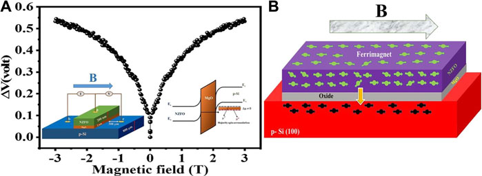
FIGURE 11. (A) Response of ΔV (spin accumulation in p-Si) at 300 K with the applied longitudinal magnetic field with a constant bias current of 5 µA. The inset on the left side depicts the three-terminal Hanle geometry. The inset on the right side illustrates the energy-band profile of the NZFO/MgO tunnel contact with p-Si. (B) Spin accumulation and spin-splitting of electrochemical potential in the Si valence band are caused by the injection of spin-polarized holes.
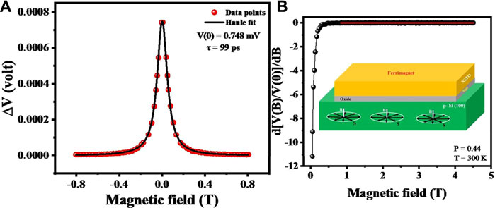
FIGURE 12. (A) The Lorentzian fit of the Hanle curve at 300 K with a bias current of 5 µA. (B) The linear fit to the first-order derivative of Eq. 6 to get the value of spin polarization. The inset shows that the perpendicular magnetic field suppresses the spin accumulation in p-Si.
Here, τ is the spin relaxation time or spin lifetime (Maji and Nath, 2020; Maji and Nath, 2019). The obtained Hanle signal can be best fitted by Eq. 5 (Figure 12A), and the spin lifetime of 99 ps has been achieved at 300 K. Comparing with the result of NFO/MgO/p-Si (Maji et al., 2021), we can confirm that the room temperature spin lifetime in p-Si is enhanced by almost 142% by using the NZFO/MgO/p-Si heterostructure. Enhanced spin polarization of NZFO may be one of the possible reasons for getting this higher value of spin lifetime in our device. The spin diffusion length of 276 nm in p-Si has been calculated from the spin lifetime using the equation LSD =
The graph of
Furthermore, a nonmagnetic Ag film has been grown on the MgO/p-Si substrate to construct and study the three-terminal Hanle experiment for assuring the pure spin accumulation in p-Si. No Hanle signal rather than some random fluctuation has been detected after the application of transverse magnetic field. This finding reinforces that the detected 3-T Hanle signal originated from the NZFO/MgO/p-Si heterostructure is solely caused by the accumulation of spins in the semiconductor injected from the ferrimagnetic NZFO film.
In a nutshell, we conclude that the optimized NZFO/MgO/p-Si heterojunction has been successfully fabricated using the PLD technique. From the structural study, we have confirmed that the NZFO film has been grown with a mixed spinel ferrite structure with no impurity phase. The M-H measurement validates that the film is ferrimagnetically soft along the in-plane direction of the film. We infer from the investigation of the transport property that our NZFO/MgO/p-Si heterojunction can operate as a conventional rectifying magnetic diode. The root of exhibiting positive magnetoresistance in our heterojunction has been best described by the standard spin injection model. The room temperature electrical spin injection, accumulation, and detection have been investigated using the NZFO/MgO tunnel contact employing 3-T Hanle geometry. The parameters such as spin lifetime (99 ps), spin diffusion length (276 nm), and spin polarization (0.44) have been estimated from the Hanle curve detected in our heterostructure at room temperature. Comparing with the result of NFO/MgO/p-Si, we can confirm that the room temperature spin lifetime in p-Si is enhanced by almost 142% by using the NZFO/MgO/p-Si heterostructure. As a consequence, these results indicate that the NZFO/MgO/p-Si heterojunction can be one of the promising candidates for rectifying a magnetic diode-like spin injecting device that has the potential to play a significant role in future spintronics device applications.
The crystallographic data presented in the study are deposited in the Figshare repository. DOI: https://doi.org/10.6084/m9.figshare.16578932.v1.
NM has majorly contributed to this paper through sample synthesis, characterization, data analysis, and manuscript writing. SS has contributed to this paper through data plotting, schematic diagram drawing, and analysis. TKN is the corresponding author who has supervised the whole project.
The authors declare that the research was conducted in the absence of any commercial or financial relationships that could be construed as a potential conflict of interest.
All claims expressed in this article are solely those of the authors and do not necessarily represent those of their affiliated organizations, or those of the publisher, the editors and the reviewers. Any product that may be evaluated in this article, or claim that may be made by its manufacturer, is not guaranteed or endorsed by the publisher.
The authors acknowledge the Central Research Facility (CRF) of IIT Kharagpur for having the necessary facilities for conducting numerous measurements and completing this study successfully. TKN would like to acknowledge IIT Kharagpur (IIT/SRIC/PHY/UBF/2014-15/137) for the financial assistance through the SGIRG challenge grant project with project code UBF.
The Supplementary Material for this article can be found online at: https://www.frontiersin.org/articles/10.3389/fmats.2021.721031/full#supplementary-material
Buchwald, W. R., and Johnson, N. M. (1988). Revised Role for the Poole-Frenkel Effect in Deep‐level Characterization. J. Appl. Phys. 64, 958–961. doi:10.1063/1.341907
Butler, W. H. (2008). Tunneling Magnetoresistance from a Symmetry Filtering Effect. Sci. Tech. Adv. Mater. 9, 014106. doi:10.1088/1468-6996/9/1/014106
Chakraborty, G., Chattopadhyay, S., Sarkar, C. K., and Pramanik, C. (2007). Tunneling Current at the Interface of Silicon and Silicon Dioxide Partly Embedded with Silicon Nanocrystals in Metal Oxide Semiconductor Structures. J. Appl. Phys. 101, 024315. doi:10.1063/1.2425290
Chen, Y. Z., Sun, J. R., Xie, Y. W., Wang, D. J., Lu, W. M., Liang, S., et al. (2007). Rectifying Properties of Magnetite-Based Schottky Diode and the Effects of Magnetic Field. Appl. Phys. Lett. 90, 143508. doi:10.1103/PhysRevB.71.18040610.1063/1.2719614
Chu, X., Jiang, D., and Zheng, C. (2007). The Preparation and Gas-Sensing Properties of NiFe2O4 Nanocubes and Nanorods. Sensors Actuators B: Chem. 123 (2), 793–797. doi:10.1016/j.snb.2006.10.020
Cullity, B. D., and Graham, C. D. (2011). Introduction to Magnetic Materials Hoboken, NJ, United States: John Wiley & Sons.
Cunningham, C. H., Arai, T., Yang, P. C., McConnell, M. V., Pauly, J. M., and Conolly, S. M. (2005). Positive Contrast Magnetic Resonance Imaging of Cells Labeled with Magnetic Nanoparticles. Magn. Reson. Med. 53 (5), 999–1005. doi:10.1002/mrm.20477
Dash, S. P., Sharma, S., Le Breton, J. C., Peiro, J., Jaffr`es, H., George, J-M., et al. (2011). Spin Precession and Inverted Hanle Effect in a Semiconductor Near a Finite-Roughness Ferromagnetic Interface. Phys. Rev. B 84, 054410. doi:10.1103/physrevb.84.054410
Dionne, G. F., and West, R. G. (1987). Magnetic and Dielectric Properties of the Spinel Ferrite System Ni0.65Zn0.35Fe2−xMnxO4. J. Appl. Phys. 61, 3868–3870. doi:10.1063/1.338623
Emori, S., Yi, D., Crossley, S., Wisser, J. J., Balakrishnan, P. P., Khodadadi, B., et al. (2018). Ultralow Damping in Nanometer-Thick Epitaxial Spinel Ferrite Thin Films. Nano Lett. 18, 4273–4278. doi:10.1021/acs.nanolett.8b01261
Ganichev, S. D., Ziemann, E., Prettl, W., Yassievich, I. N., Istratov, A. A., and Weber, E. R. (2000). Distinction between the Poole-Frenkel and Tunneling Models of Electric-Field-Stimulated Carrier Emission from Deep Levels in Semiconductors. Phys. Rev. B 61, 10361–10365. doi:10.1103/PhysRevB.61.10361
Köhler, U., Ziese, M., Bollero, A., Höhne, R., and Esquinazi, P. (2004). On the Road to an All-Oxide Spin-Transistor: Study of Magnetotransport Properties of magnetite/Nb:STO Interfaces. J. Magnetism Magn. Mater. 272-276, E1437–E1438. doi:10.1016/j.jmmm.2003.12.447
Kumbhar, S. S., Mahadik, M. A., Mohite, V. S., Rajpure, K. Y., and Bhosale, C. H. (2014). Synthesis and Characterization of Spray Deposited Nickel-Zinc Ferrite Thin Films. Energ. Proced. 54, 599–605. doi:10.1016/j.egypro.2014.07.301
Li, Y., Liu, X., Kan, X., Feng, S., Lv, Q., Huang, J., et al. (2020). Investigation of Structural and Magnetic Properties of Cu-Substituted NiZn Spinel Ferrites. J. Mater. Sci. Mater. Electron. 31, 17133–17142. doi:10.1007/s10854-020-04273-y
Maji, N., Kar, U., and Nath, T. K. (2018). Spin Valve-like Magnetic Tunnel Diode Exhibiting Giant Positive junction Magnetoresistance at Low Temperature in Co2MnSi/SiO2/p-Si Heterostructure. Appl. Phys. A. 124, 156. doi:10.1007/s00339-018-1579-4
Maji, N., and Nath, T. K. (2020). Robust and Efficient Electrical Injection of Spin-Polarized Carriers from a Zero-Spin-Gap Half-Metal V2NiAl into N-Si at Room Temperature. ACS Appl. Electron. Mater. 2, 3299–3306. doi:10.1021/acsaelm.0c00625
Maji, N., and Nath, T. K. (2019). Room Temperature Electrical Spin Injection from a New Spin Gapless Ferromagnetic Semiconducting Inverse Heusler alloy Mn2CoSi into P-Si via SiO2 Tunnel Barrier. J. Appl. Phys. 125, 173903. doi:10.1063/1.5079975
Maji, N., Panda, J., Kumar, A. S., and Nath, T. K. (2021). Demonstration of Efficient Spin Injection and Detection into P-Si Using NiFe2O4 Based Spin Injector in NiFe2O4/MgO/p-Si Device. Appl. Phys. A. 127, 31. doi:10.1007/s00339-020-04214-w
McCurrie, R. A. (1994). Ferromagnetic Materials: Structure and Properties. London, United Kingdom: Academic Press.
Parkin, S. S. P., HayashiThomas, M. L., and Thomas, L. (2008). Magnetic Domain-wall Racetrack Memory. Science 320, 190–194. doi:10.1126/science.1145799
Pradhan, D. K., Misra, P., Puli, V. S., Sahoo, S., Pradhan, D. K., and Katiyar, R. S. (2014). Studies on Structural, Dielectric, and Transport Properties of Ni0.65Zn0.35Fe2O4. J. Appl. Phys. 115, 243904. doi:10.1063/1.4885420
Qu, T. L., Zhao, Y. G., Tian, H. F., Xiong, C. M., Guo, S. M., and Li, J. Q. (2007). Rectifying Property and Giant Positive Magnetoresistance of Fe3O4∕SiO2∕Si Heterojunction. Appl. Phys. Lett. 90, 223514. doi:10.1063/1.2743937
Raikher, Y. L., Stepanov, V. I., Depeyrot, J., Sousa, M. H., Tourinho, F. A., Hasmonay, E., et al. (2004). Dynamic Optical Probing of the Magnetic Anisotropy of Nickel-Ferrite Nanoparticles. J. Appl. Phys. 96 (9), 5226–5233. doi:10.1063/1.1790574
Rana, S., Srivastava, R. S., Sorensson, M. M., and Misra, R. D. K. (2005). Synthesis and Characterization of Nanoparticles with Magnetic Core and Photocatalytic Shell: Anatase TiO2-NiFe2O4 System. Mater. Sci. Eng. B 119 (2), 144–151. doi:10.1016/j.mseb.2005.02.043
Reig, C., Cardoso, S., and Mukhopadhyay, S. C. (2013). Giant Magnetoresistance (GMR) Sensors - from Basis to State-Of-The-Art Applications. Berlin/Heidelberg, Germany: Springer. doi:10.1007/978-3-642-37172-1
Seki, M., Takahashi, M., Ohshima, T., and Tabata, H. (2013). High Spin Polarization at Room Temperature in Ge-Substituted Fe3O4epitaxial Thin Film Grown under High Oxygen Pressure. Appl. Phys. Lett. 103, 212404. doi:10.1063/1.4832062
Sharma, R., Thakur, P., Kumar, M., Sharma, P., and Sharma, V. (2018). Nanomaterials for High Frequency Device and Photocatalytic Applications: Mg-Zn-Ni Ferrites. J. Alloys Compd. 746, 532–539. doi:10.1016/j.jallcom.2018.02.287
Srinivasan, T. T., Ravindranathan, P., Cross, L. E., Roy, R., Newnham, R. E., Sankar, S. G., et al. (1988). Studies on High‐density Nickel Zinc Ferrite and its Magnetic Properties Using Novel Hydrazine Precursors. J. Appl. Phys. 63, 3789–3791. doi:10.1063/1.340615
Thakur, P., Sharma, R., Sharma, V., and Sharma, P. (2017). Structural and Optical Properties of MnZnFeO Nano Ferrites: Effect of Sintering Temperature. Mater. Chem. Phys. 193, 285–289. doi:10.1016/j.matchemphys.2017.02.043
Tsybeskov, L., Grom, G. F., Fauchet, P. M., McCaffrey, J. P., Baribeau, J.-M., Sproule, G. I., et al. (1999). Phonon-assisted Tunneling and Interface Quality in Nanocrystalline Si/amorphous SiO2 Superlattices. Appl. Phys. Lett. 75, 2265–2267. doi:10.1063/1.124985
Valenzuela, R. (2012). Novel Applications of Ferrites. Phys. Res. Int. 2012, 1–9. doi:10.1155/2012/591839
Vincent, G., Chantre, A., and Bois, D. (1979). Electric Field Effect on the thermal Emission of Traps in Semiconductor Junctions. J. Appl. Phys. 50, 5484. doi:10.1063/1.326601
Wolf, S. A., Awschalom, D., Buhrman, R., Daughton, J., Von Molnar, S., Roukes, M., et al. (2001). Spintronics: a Spin-Based Electronics Vision for the Future. Science 294, 1488–1495. doi:10.1126/science.1065389
Yoon, T.-J., Kim, J. S., Kim, B. G., Yu, K. N., Cho, M.-H., and Lee, J.-K. (2005). Multifunctional Nanoparticles Possessing A ?Magnetic Motor Effect? for Drug or Gene Delivery. Angew. Chem. Int. Ed. 44 (7), 1068–1071. doi:10.1002/anie.200461910
Zabel, H., and Farle, M. (2012). Magnetic Nanostructures: Spin Dynamics and Spin Transport. Berlin/Heidelberg, Germany: Springer.
Keywords: magnetic tunnel diode, heterostructure, mixed spinel ferrite, junction magnetoresistance, spin lifetime, spin polarization, spintronics
Citation: Maji N, Shit S and Nath TK (2021) Enhanced Spin Accumulation in Semiconductor at Room Temperature Using Ni0.65Zn0.35Fe2O4(NZFO) as Spin Injector in NZFO/MgO/p-Si Device. Front. Mater. 8:721031. doi: 10.3389/fmats.2021.721031
Received: 05 June 2021; Accepted: 05 August 2021;
Published: 01 October 2021.
Edited by:
Faiz Pourarian, Carnegie Mellon University, United StatesReviewed by:
Om Prakash Sinha, Amity Institute of Nanotechnology (AINT), IndiaCopyright © 2021 Maji, Shit and Nath. This is an open-access article distributed under the terms of the Creative Commons Attribution License (CC BY). The use, distribution or reproduction in other forums is permitted, provided the original author(s) and the copyright owner(s) are credited and that the original publication in this journal is cited, in accordance with accepted academic practice. No use, distribution or reproduction is permitted which does not comply with these terms.
*Correspondence: T. K. Nath, dG5hdGhAcGh5LmlpdGtncC5lcm5ldC5pbg==
Disclaimer: All claims expressed in this article are solely those of the authors and do not necessarily represent those of their affiliated organizations, or those of the publisher, the editors and the reviewers. Any product that may be evaluated in this article or claim that may be made by its manufacturer is not guaranteed or endorsed by the publisher.
Research integrity at Frontiers
Learn more about the work of our research integrity team to safeguard the quality of each article we publish.