 Di Sun1
 Yu Fang
 Wenjun Sun
94% of researchers rate our articles as excellent or good
Learn more about the work of our research integrity team to safeguard the quality of each article we publish.
Find out more
ORIGINAL RESEARCH article
Front. Mater., 13 September 2021
Sec. Quantum Materials
Volume 8 - 2021 | https://doi.org/10.3389/fmats.2021.717760
This article is part of the Research TopicLight-Nanomaterial Interactions for Energy Efficient Nanophotonic DevicesView all 10 articles
Graphene/MoS2/Ag thin films were successfully prepared by the magnetron sputtering technique and liquid phase exfoliation. Structure, morphology, optical properties, and nonlinear optical characteristics of the graphene/MoS2/Ag and graphene/MoS2 thin films were studied by X-ray diffractometer, spectrophotometer, field-scanning electron microscope, and femtosecond (fs) Z-scan technique. The results of the fs Z-scan experiment indicate that the graphene/MoS2/Ag thin films exhibit reverse saturable absorption properties due to the free carrier absorption and two-photon absorption. More importantly, with the increase of DC magnetron sputtering power (from 5 to 15 W), the local surface plasmon resonance effect of the Ag thin films increases, which leads to the enhancement of nonlinear optical properties of the graphene/MoS2/Ag thin films. The nonlinear absorption coefficients of the graphene/MoS2/Ag thin films are increased from 1.14 × 10⁻¹⁰ to 1.8 × 10⁻¹⁰ m/W at 800 nm and from 4.79 × 10⁻¹¹ to 6.79 × 10⁻¹¹ m/W at 1,030 nm, and the nonlinear refraction index of the graphene/MoS2/Ag thin films is -4.37 × 10⁻¹⁷∼−4.18 × 10⁻¹⁶ m2/W under the excitation of 800 and 1,030 nm, respectively. Moreover, when the graphene/MoS2/Ag thin films were excited at 800 and 1,030 nm, respectively, the nonlinear figure of merit values of the graphene/MoS2/Ag thin films are increased from 1.23 to 2.91 and from 1.30 to 1.47, which are enough to support the application of the graphene/MoS2/Ag thin films in the field of all-optical switching applications.
In recent years, graphene is widely studied due to its large carrier mobility and high optical absorption property (Katsnelson et al., 2009; Gao et al., 2019). However, the zero band gap property limits the research and application of graphene in the optoelectronics field. As the research develops in depth, it can be found that the emergence of graphene composite systems can solve this issue. Among these, they exhibit superior optical, electrical, and chemical properties to graphene; thus, the graphene/MoS2 nanocomposites have been extensively studied (Fu et al., 2014; Yu et al., 2014; Kwon and Kim, 2018). Compared with graphene, the graphene/MoS2 nanocomposites exhibit higher photoresponse (Zhang et al., 2014), higher dielectric constant, and higher linear absorption (Jiang et al., 2015; He et al., 2017; Qiu et al., 2018; Sun et al., 2018; Xu et al., 2020) due to the excellent properties of the graphene/MoS2; the graphene/MoS2 nanocomposites can be widely used in the manufacture of dye-sensitized solar cells, electrical sensors, and transistors (Liu et al., 2012; Huang et al., 2013; He et al., 2014). In the field of nonlinear optics, the reverse saturable absorption (RSA) property, which is shown by graphene/MoS2 thin film, shows that the light transmittance decreases with the increase of incident light (Ouyang et al., 2013), and it can be widely used in all optical switches, optical sensors, and other fields (Vabbina et al., 2015; Chen et al., 2016; Iqbal et al., 2019). Nevertheless, graphene/MoS2 thin films still face many challenges, such as nonlinear response and high nonlinear figure of merit (FOM) values.
To further raise the nonlinear broadband optical response of graphene/MoS2 thin film and increase the wide application in all optical devices, a novel structure was designed here, and it uses the noble metal to composite the graphene/MoS2 thin films. Among the numerous noble metals, silver was chosen to composite the graphene/MoS2 thin films due to its localized surface plasmon resonance (LSPR) effect, which can effectively capture photogenerated carriers and restrain the recombination between carriers and holes (Li et al., 2007; Zheng et al., 2007; Akhavan, 2009; Charles et al., 2009; Jiang et al., 2012). In addition, the LSPR effect of Ag can provide more free carriers to construct free carrier absorption (FCA) in the graphene/MoS2/Ag thin films, and the FCA can effectively promote the excited state absorption at near infrared, thus leading to the nonlinear optical response move to broadband. Moreover, the addition of Ag has a good composite significance, because of which it can effectively regulate the optical band gap of the graphene/MoS2/Ag thin films and promote the FCA and TPA (Shahriari et al., 2017). Therefore, the closed-aperture (CA) Z-scan signals of the graphene/MoS2/Ag thin films were obtained at near infrared due to the free carrier refraction (FCR), which is constructed by the free carriers provided by the LSPR effect of Ag. Moreover, the nonlinear absorption coefficient and nonlinear refractive index of the graphene/MoS2/Ag thin films were obtained from the broadband nonlinear signals of the graphene/MoS2/Ag thin films, which is of great significance for evaluating the nonlinear FOM value and the application of all-optical switches. With the composite of Ag, the nonlinear FOM values of graphene/MoS2/Ag thin films can be improved successfully and can be widely used in all-optical switching devices.
In this work, graphene/MoS2/Ag thin films with different magnetron sputtering power in the Ag target (5, 10, and 15 W), and graphene/MoS2 thin films were successfully prepared by using magnetron sputtering technology and liquid phase exfoliation. The graphene/MoS2/Ag thin films show a broadband nonlinear optical response, larger nonlinear absorption coefficient, and higher nonlinear refractive index at near infrared, and the nonlinear absorption coefficient and nonlinear refractive index of the graphene/MoS2/Ag thin films can be determined by the content of the Ag thin films. The nonlinear absorption coefficients of graphene/MoS2/Ag thin films (from 5 to 15 W) are from 1.14 × 10⁻¹⁰ to 1.8 × 10⁻¹⁰ m/W at 800 nm and from 4.79 × 10⁻¹¹ to 6.79 × 10⁻¹¹ m/W at 1,030 nm, respectively. The nonlinear refractive index of the graphene/MoS2/Ag thin films (from 5 to 15 W) are from –1.12 × 10⁻¹⁶ to –4.18 × 10⁻¹⁶ m2/W at 800 nm and from –4.37 × 10⁻¹⁷ to –8.00 × 10⁻¹⁷ m2/W at 1,030 nm, respectively. Moreover, the nonlinear FOM values of graphene/MoS2/Ag thin films (from 5 to 15 W) are from 1.23 to 2.91 at 800 nm and from 1.30 to 1.47 at 1,030 nm. Surprisingly, compared with the graphene/MoS2 thin film, the FOM values of the graphene/MoS2/Ag thin films are successfully improved under the same excitation conditions, which can be widely used in all-optical switching devices.
The sputtering target of Ag (99.99% purity, 6.0 cm diameter, 0.6 cm thickness) was purchased from Hebei Qinbang New Material Technology Co. The filter membranes (220 nm diameter) that were used to deposit graphene/MoS2 thin films were purchased from Tianjin Jinteng Co. Ltd. The flake graphite used for the liquid phase exfoliation technique was purchased from Sinopharm Chemical Reagent Co. Ltd. The MoS2 used for the liquid phase exfoliation technique was purchased from Shanghai Acmec Biochemical Co. Ltd. The N-methyl-2-pyrrolidone solvent (NMP) used for the dispersant of graphene/MoS2 was purchased from Tian in Fuyu Fing Chemical Co. Ltd.
The Ag thin films were precisely deposited on the sapphire substrate by direct current (DC) magnetron sputtering. The sapphire substrate was, respectively, washed by anhydrous ethanol, deionized water, and acetone for 15 min until the substrate was completely clean and then dried at room temperature. The precise sputtering power of 5, 10, and 15 W in the Ag target can be achieved by regulating the magnetron sputtering conditions (current and voltage). During the deposition, high-purity argon was employed as a working gas (purity 99.999 vol%) with a gas flow rate of 20 sccm, and the working pressure was 1.0 Pa, the sputtering time was 35 s, the sputtering temperature was 25°C, and the vacuum of the sputtering room was 5.5 × 10⁻⁴ Pa.
The graphene/MoS2 thin films were prepared by the liquid phase exfoliation technology. The NMP is widely used as the dispersing agent for the graphene and MoS2 in the report; thus, the NMP was selected as the dispersing agent for the graphene/MoS2 (Kim et al., 2015; Hua et al., 2017; Qi et al., 2017). The graphite and MoS2 powders at a weight ratio of 1:1 were dispersed in NMP to fabricate dispersion. The concentration of the dispersion was 0.2 mg/ml. Then, the dispersion was sonicated for 1–2 h at a high power of 600 W, which can produce such a result that the graphite and the MoS2 are well exfoliated. The obtained suspension was centrifuged at 6,000 rpm/min for 1 h, and half of the supernatant was extracted. The formation of the graphene/MoS2 thin films were made by using 40 ml supernatant to be deposited on the 220 nm pore size membranes by a vacuum filtration technique and then naturally dried at room temperature.
Then, the dried films were put upside down on the prepared Ag thin films and pressure applied with a 2 kg weight to make the graphene/MoS2 thin films better fit on the Ag thin films. The weight was removed after 2 h, and then the graphene/MoS2/Ag thin films (with the filter membranes) were washed with the acetone, which was used to remove the filter membranes. After washing, the graphene/MoS2/Ag thin films were placed at room temperature and then dried naturally for 1 h, and finally, the graphene/MoS2/Ag thin films were successfully prepared. The schematic diagram of the graphene/MoS2/Ag thin film preparation process is shown in Figure 1. To make the expression more concise, A and B are used to represent the graphene/MoS2 and the graphene/MoS2/Ag thin films, where B1, B2, and B3 are, respectively, used to represent the graphene/MoS2/Ag (5, 10, and 15 W) thin films.
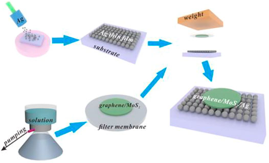
FIGURE 1. Graphene/MoS2/Ag thin film preparation process and structure diagram.
The morphology and thickness of A and B thin films were observed by field-scanning electron microscope (FE-SEM) (SU70, Hitachi, Japan), the X-ray diffractometer (XRD) pattern was characterized by XRD (D8, Bruker, Germany), and the linear absorption spectrum of A and B thin films was characterized by spectrophotometer (Uv-Vis) (Uv-3600i PLUS, SHIMADZU, Japan).
The nonlinear optical characteristics of A and B thin films were tested by femtosecond (fs) Z-Scan experiments. The light source used an optical parameter amplifier (Light Conversion ORPHEUS), which was pumped by a mode-locked Yb:KGW fiber laser. The measurement parameters were set at 190 fs pulse and 20 Hz, and the waist radius of the laser was 33 µm. The energies of the laser excitation were set at 400, 500, and 600 nJ, respectively. The fs Z-scan experiment was carried out with the device described in the report (Wang et al., 2001; Yao et al., 2013).
Figure 2 shows the XRD patterns of A and B thin films. The XRD patterns show that A and B thin films both present the polycrystalline structure. For the A thin film, compared with the XRD standard card (PDF#17-0744), the diffraction characteristic peak of MoS2 (003) was detected at 14.53° (2θ) with the lattice spacing of 6.09 nm. The diffraction characteristic peak of graphene (002) was detected at 26.6° (2θ) with the lattice spacing of 3.69 nm (PDF#41-1,487), which is consistent with reports in the literature; it can be confirmed that the graphene is successfully prepared by liquid phase exfoliation (Wang et al., 2017). For the B thin films with the successful composite of the Ag thin films, the diffraction characteristic peaks of graphene (002) and MoS2 (003) were enhanced; the diffraction characteristic peak of Ag (200) was detected at 44.27° (2θ) with the lattice spacing of 2.038 nm (PDF#04–0783). Compared with the XRD standard card (PDF#17-0744), the diffraction characteristic peak of MoS2 (006) was also detected at 29.35° (2θ) with the lattice spacing of 3.04 nm. In addition, the increase of magnetron sputtering power in the Ag target induces the enhancement of the diffraction characteristic peaks of Ag (200), and the highest XRD intensity was obtained at the B thin film (15 W). Moreover, we also calculated the lattice constants of graphene, MoS2, and Ag in the B thin film, which are 6.64, 3.16, and 4.08 nm, respectively, in which the lattice constant of MoS2 is consistent with the few layers MoS2 in the report (Ghadiyali and Chacko, 2019; Qi et al., 2019; Cior et al., 2020). The obtained results are consistent with the literature. The results of the XRD pattern show that the B thin films are successfully prepared.
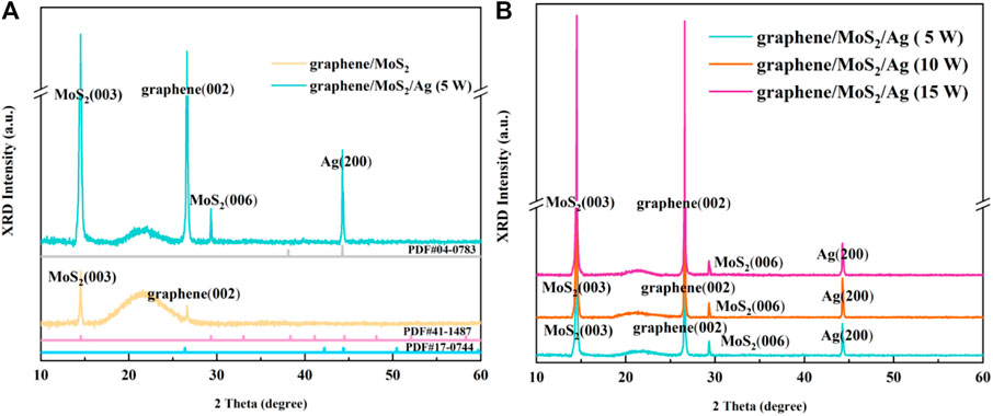
FIGURE 2. (A) The XRD patterns of the A and B thin films (5 W). (B) The XRD patterns of the B thin films (from 5 to 15 W).
The morphologies and thicknesses of the Ag thin films under different DC magnetron sputtering powers were obtained by SEM as shown in Figures 3A–C. The distribution of Ag nanoparticles in the Ag thin films are uniform, and with the increase of magnetron sputtering power, the size of the Ag particles increases accordingly. In addition, the average Ag particle size of the Ag thin films under different DC magnetron sputtering power was also calculated as 18 (5 W), 24 (10 W), and 30 nm (15 W), respectively. Figures 3D–F exhibit the thickness of the Ag films. With the increase of the magnetron sputtering power, the thickness of the Ag thin films increases from 50 to 90 nm.
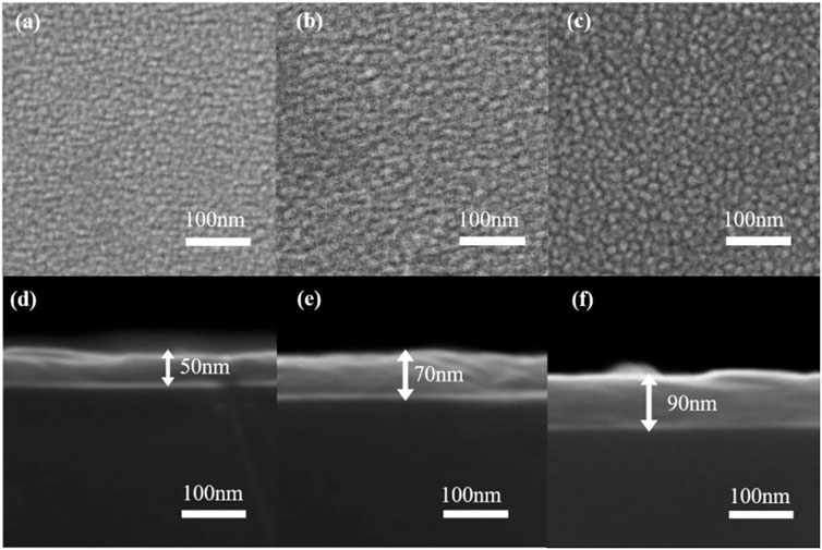
FIGURE 3. (A) The morphology of the Ag thin film under 5 (A), 10 (B), and 15 W (C) DC magnetron sputtering power. (D) The thickness of the Ag thin film under 5 (D), 10 (E), and 15 W (F) DC magnetron sputtering power.
The morphology and thickness of the B thin films were characterized by SEM as shown in Figure 4. To observe the morphology of the B thin films more intuitively, the edge of the A thin film was selected for shooting so as to distinguish between the Ag thin film and the graphene/MoS2 thin film as shown in Figure 4A. In addition, the thickness of the B thin films (from 5 to 15 W) was characterized by SEM and is shown in Figure 4B–D. The thickness of the B thin films is 350, 370, and 390 nm, respectively, which corresponds to the B thin films with the different magnetron sputtering power of 5, 10, and 15 W, respectively. It can be seen from the SEM that the successful composite of Ag thin films improves the thickness of the B thin films. It can be inferred that the thickness of graphene/MoS2 thin film is 300 nm. In past reports, the absorption of the composite films is enhanced with the increase of the content of Ag films; thus, we preliminarily infer that the absorption of the graphene/MoS2/Ag thin films is enhanced with the increase of the thickness of the Ag thin films.
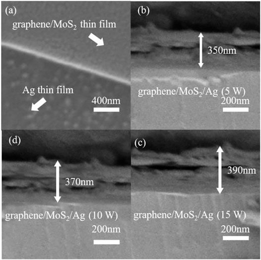
FIGURE 4. (A) The morphology of the B thin film and the thickness of the B1(B), B2(C), and B3(D) thin films.
The linear absorption and transmission spectrums of the A and the B thin films were tested by spectrophotometer as shown in Figure 5. It can be seen from Figure 5A that A and B thin films exhibit two obvious absorption peaks, which are caused by the two exciton transition absorption peaks A and B at the Brillouin K/K′ point due to the direct band gap transition of MoS2 (Yin et al., 2019). In addition, with the increase of the magnetron sputtering power in the Ag target, the absorption peak of the B thin films exhibits a tendency of red shift that is consistent with the report by Yang et al., and it can be seen from the report that the light absorption of metal nanoparticles is affected by the size of the metal nanoparticles, and the conclusion is that the size of the Ag nanoparticles in Ag thin films can be affected by the increase of the magnetron sputtering power in the Ag target, which was given in SEM. With the increase of the magnetron sputtering power in the Ag target, the size of the Ag nanoparticles increases. The increase of the size of the Ag nanoparticles can lead to the lattice contraction of the nanoparticles, which leads to the decrease of the resonance frequency of the surface plasmons. Thus, the absorption peak of the B thin films is red shifted. In addition, with the composite of the Ag thin films, the LSPR effect of the Ag nanoparticles can lead to the electron filling of graphene/MoS2 bang; thus, the overall bang gap of the B thin films decreases, leading to an increased absorption of the B thin films. This result confirms the correct inference that the absorption of the B thin films increases as the thickness of the Ag thin films increases. For the linear absorption, we have that Tacu’s formulation is given as follows (Qian et al., 2014):
where α is the coefficient of linear absorption, A is a constant, n is an index (n = 1, 2, 3), hν is the energy of the incident photon, and Eg is the optical bandwidth. The optical band width of A and B thin films were calculated as 1.77 eV, 1.73 eV (5 W), 1.70 eV (10 W), and 1.62 eV (15 W), respectively. Figure 5B exhibits the transmission spectrum of the A and B thin films. It can be clearly seen that the A and B thin films both exhibit more than 65% transmission in the range of 800–1,050 nm, and the composite of Ag thin films has no effect for the transmittance at near infrared.
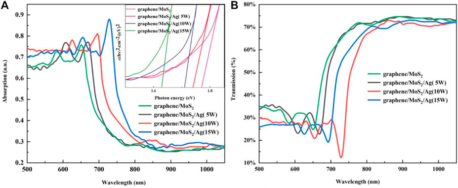
FIGURE 5. The linear absorption (A) and transmission (B) of the A and B thin films.
To further understand the mechanism of nonlinear response and regulation, the nonlinear signals of the A and B thin films were obtained by using the fs Z-scan technique at 800 and 1,030 nm. The Z-scan curve shows a smooth valley shape, and it is symmetric to the focal point (Z = 0), which confirms that the main nonlinear absorption characteristics of the A and B thin films are the RSA characteristic. The open-aperture (OA) Z-scan results of the A and B thin films are shown in Figures 6A,B. The A thin film exhibited RSA properties at 800 nm although no signal was observed at 1,030 nm. It can be seen from the linear spectrum that the Eg of the A and B thin films is greater than hv but less than 2hv; thus, the A and B thin films all exhibit a TPA characteristic (Honda et al., 2011). The OA Z-scan signals of the B thin films were observed at 1,030 nm. Moreover, with the increment of the DC magnetron sputtering power in the Ag target (from 5 to 15 W), the amplitude of the OA Z-scan signals of the films exhibited a corresponding increase. In addition, to study the relationship between the laser intensity and the nonlinear signal of the A and B thin films, the A and B3 thin films were excited at 800 and 1,030 nm with different laser energy, as is shown in Figures 6C,D. For the A thin film, with the increase of the excitation laser energy, the OA Z-scan signal of the A thin film had no change; thus, it is confirmed that the A thin film exhibits a pure third-order nonlinear effect, which is caused by the absorption of the excited state induced by the TPA. For the B3 thin film, with the increase of the laser energy, the amplitude of the OA Z-scan signal increased. In combination with the OA Z-scan signals of the B thin films, which were obtained by changing the DC magnetron sputtering power in the Ag target (5–15 W), thus, we infer that there is a high-order nonlinear absorption effect in the nonlinear absorption phenomenon of the B thin films. For the high-order nonlinear absorption phenomenon, we have (Chen and Zhao, 2018)
Here, α is the global absorption coefficient, γ is the fifth-order nonlinear absorption coefficient, T(z) stands for the normalized transmittance, β is the nonlinear absorption coefficient of the thin films, and I0 is the light intensity at the focus. The effective thickness of the thin films is denoted by Leff, and the Leff can be calculated by
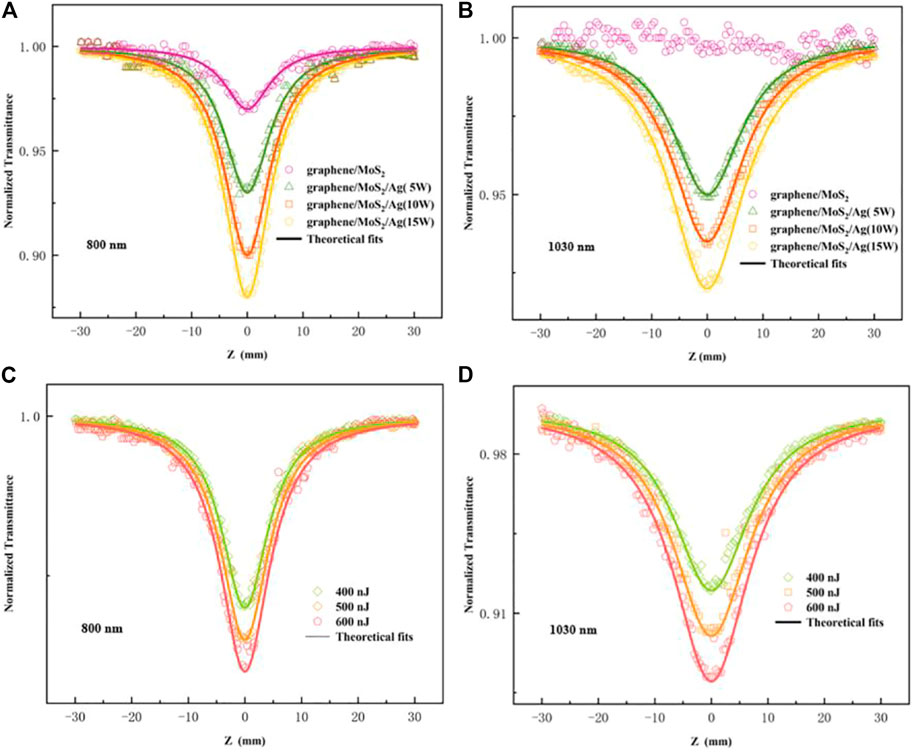
FIGURE 6. The OA Z-scan signals of A and B thin films at 800 (A) and 1,030 nm (B). The OA Z-scan signals of B3 thin film at 800 (C) and 1,030 nm (D) under different excitation conditions.
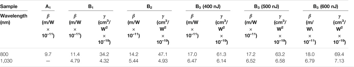
TABLE 1. Nonlinear absorption parameters of the A and B thin films under different excitation conditions.
It can be seen from the calculation results of the nonlinear absorption coefficient of the B thin films that, with the increase of the laser energy, the nonlinear absorption coefficients of the B thin films exhibit the corresponding increase; thus, our inference is confirmed. The reason for the high-order nonlinear absorption effect can be attributed to the FCA, which is caused by the composite of the Ag thin films.
For Ag nanoparticles, the LSPR effect on their surface can effectively increase the interaction between light and matter, promote the separation of photogenerated carriers and holes, and can effectively capture photogenerated carriers (Xiang et al., 2012; Xi et al., 2014; Agrawal et al., 2018; Ye et al., 2019). When the Ag thin films are successfully composited with the graphene/MoS2 thin film, it can provide more carriers for the B thin film; thus, the FCA is constructed in the excited state, so a combination of FCA and TPA is successfully presented, and thus, the nonlinear absorption effect of the B thin films is enhanced. In addition, with the increment of DC magnetron sputtering in the Ag target, Ag thin films that were prepared by different DC magnetron sputtering power can provide more Ag nanoparticles and then provide more photogenerated carriers to enhance the FCA effect; thus, the excited state absorption and RSA behavior of B thin films are enhanced. The energy level diagram of B thin film is shown in Figure 7. The τ1 can be attributed to the radiative relaxation of carriers from the conduction band to the valence band. The τ2 can be attributed to the cooling of the carriers in the conduction band.
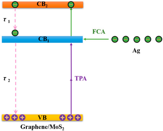
FIGURE 7. The energy level diagram of the graphene/MoS2/Ag thin film.
Figures 8A,B show the CA Z-scan signals that were obtained by the A and B thin films at 800 and 1,030 nm. For the A thin film, the CA Z-scan signal was only observed at 800 nm, which can be attributed to Kerr refraction caused by the nonlinear systematic dispersion of bound electrons appearing near the intrinsic absorption edge, and there was no CA Z-scan signal observed at 1,030 nm, which can be caused by the weak Kerr refraction. For the B thin films, the CA Z-scan signals were both observed at 800 and 1,030 nm, which exhibits the existence of high-order nonlinear refraction. In addition, the amplitude of the CA Z-scan signals increases with the increase of the DC magnetron sputtering power in the Ag target at 800 and 1,030 nm. According to the results of the OA Z-scan signals, with the increase of the DC magnetron sputtering power in the Ag target, more Ag nanoparticles can be provided by Ag thin films, which leads to the increase of the photogenerated carriers. Therefore, it can be summarized that the content of the photogenerated carriers in the B thin films is relatively high, and the excess photogenerated carriers can participate in the refraction effect of free carriers. Thus, it can be inferred that the FCR effect at 1,030 nm is the dominant effect. According to the plasma dispersion effect of carriers, the refraction effect of free carriers increase with the increase of incident wavelength (Sameshima et al., 2009; Soref and Bennett, 1987). Therefore, the B thin films exhibit a self-defocusing behavior at 1,030 nm, which is constructed by the free carrier reflection and Kerr refraction. In addition, we also obtained the CA Z-scan signals of the A and B3 thin films, which were excited at different laser energy as shown in Figures 8C,D. For the A thin film, there was no CA signal change. For the B3 thin film, the signals of the CA Z-scan indicate that the amplitude of the nonlinear signal increases with the increase of the laser energy. The reason for the phenomenon is that, with the increase of the laser energy, excess carriers are generated, and they can participate in the refraction of the free carriers, thus leading to the enhancement of the FCR (Fang et al., 2015). For nonlinear refraction, we assume that the incident laser has a Gaussian distribution, and then, the sample transmittance on the far-field axis is proportional to the phase shift (Gao et al., 2005).
The effective thickness of the samples is denoted by Leff and
The values of n2 can be calculated by using Eq. 4–6. The calculated results of n2 are shown in Table 2. The calculated results agree with our inference and confirm our point.
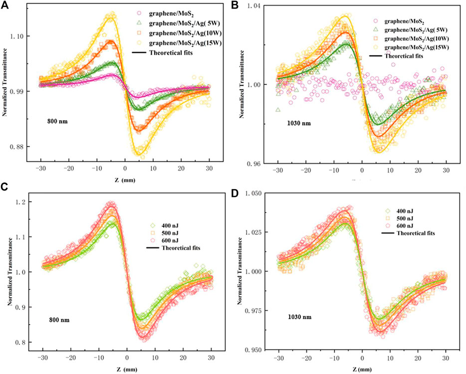
FIGURE 8. The CA Z-scan signal of A and B thin films at 800 (A) and 1,030 nm (B). The CA Z-scan signals of B3 thin film at 800 (C) and 1,030 nm (D) under different excitation conditions.
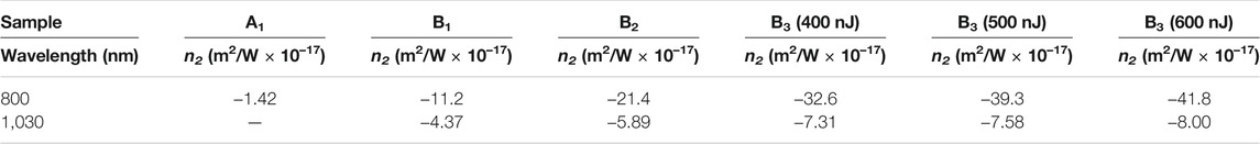
TABLE 2. Nonlinear refraction index of the A and the B thin films under different excitation conditions.
According to the analysis of the signals of the OA and CA Z-scans, the B thin films have the potential to be applied in the fields of nonlinear all-optical switching and optical limiters. Therefore, for nonlinear all-optical switches, one of the core criteria is the nonlinear FOM. Here, the FOM values of A and B thin films under different energy excitation at 800 and 1,030 nm are calculated to judge their advantages and disadvantages in the application of all-optical switches. For the nonlinear FOM value, we have (7) (Sheik-Bahae et al., 1990)
where n2 is the nonlinear refractive index, β is the nonlinear absorption coefficient, and λ is the excitation wavelength. Compared with the FOM value of the A thin film (0.15) at 800 nm, the FOM values of the B1, B2, and B3 thin films are successfully improved at 800 nm, and the nonlinear FOM value were calculated as 1.23, 1.88, and 2.39, respectively. In addition, the nonlinear FOM values of the B1, B2, and B3 thin films at 1,030 nm are also calculated as 1.30, 1.35, and 1.42, respectively. With the increase of magnetron sputtering power in the Ag target, the values of nonlinear FOM of the B thin films exhibit a corresponding increase at 800 and 1,030 nm. In addition, with the increase of the laser intensity, the values of nonlinear FOM of the B3 thin film also exhibit a corresponding increase up to the maximum numbers of 2.91 and 1.47 at 800 and 1,030 nm. Compared with other materials, the B3 thin film exhibits an excellent value of the nonlinear FOM. The results of the value of nonlinear FOM are shown in Table 3.
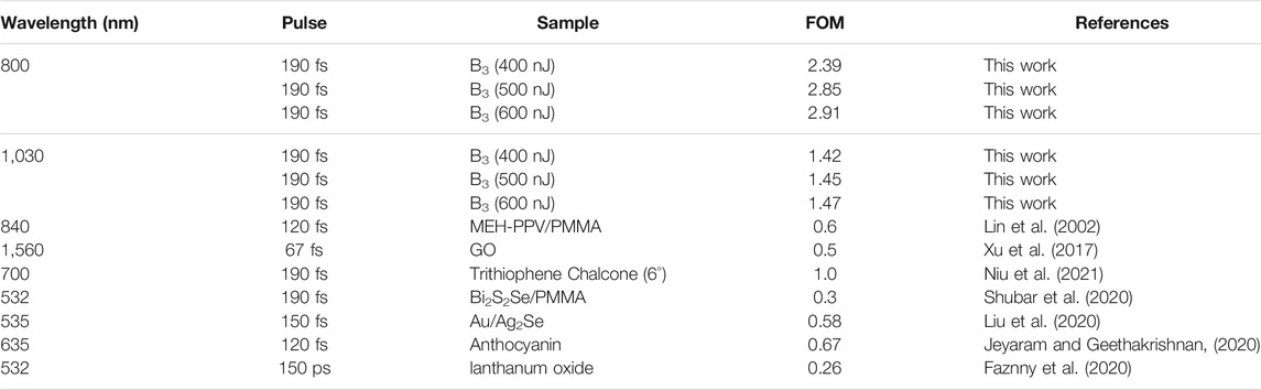
TABLE 3. The nonlinear figure of merit (FOM) of different materials.
In summary, the study confirms that, with the composite of the Ag thin films, the nonlinear response of the graphene/MoS2/Ag thin films is successfully constructed at near infrared. In addition, we also confirm that FCA and TPA are the main reasons for the nonlinear absorption enhancement of the graphene/MoS2/Ag thin films, and the Kerr refraction and the FCR are the main reasons for the formation of nonlinear refraction of graphene/MoS2/Ag thin films at near infrared. Compared with graphene/MoS2 thin films, the graphene/MoS2/Ag thin films exhibit a significant broadband nonlinear response at near infrared and the higher nonlinear absorption coefficients that are from 4.79 × 10⁻¹¹ to 1.8 × 10⁻¹⁰ m/W at 800 and 1,030 nm and the higher nonlinear refraction index, which is from −4.37 × 10⁻¹⁷ to −4.18 × 10⁻¹⁶ m2/W at 800 and 1,030 nm. More importantly, the broadband nonlinear response, nonlinear absorption coefficients, and nonlinear refraction index can be determined by the amount of the composite of the Ag thin films. Moreover, the graphene/MoS2/Ag thin films exhibit the superior value of the nonlinear FOM and the maximum value of nonlinear FOM is 2.85. The result provides the possibility for the fabrication of all-optical switch at near infrared.
The original contributions presented in the study are included in the article/Supplementary Material, further inquiries can be directed to the corresponding author.
DS contributed to conception and design of the study. WS organized the database. DS wrote the first draft of the manuscript. DS, YF, XY, WJS, and QM wrote sections of the manuscript. All authors contributed to manuscript revision, read, and approved the submitted version.
This work is supported by the National Natural Science Foundation of China (Grant No. 11504072), Natural Science Foundation of Heilongjiang Province (Grant No. LH 2020F032) and (Grant LH 2019A018); Key Laboratory for Photonic and Electronic Bandgap Material (Ministry of Education) and School of Physics and Electronic Engineering of Harbin Normal University of China, National Natural Science Foundation of China (No. 11704273) and Natural Science Foundation of Jiangsu Province, China (Grant No. BK20170375)
The authors declare that the research was conducted in the absence of any commercial or financial relationships that could be construed as a potential conflict of interest.
All claims expressed in this article are solely those of the authors and do not necessarily represent those of their affiliated organizations, or those of the publisher, the editors and the reviewers. Any product that may be evaluated in this article, or claim that may be made by its manufacturer, is not guaranteed or endorsed by the publisher.
Agrawal, A., Cho, S. H., Zandi, O., Ghosh, S., Johns, R. W., and Milliron, D. J. (2018). Localized Surface Plasmon Resonance in Semiconductor Nanocrystals. Chem. Rev. 118, 3121–3207. doi:10.1021/acs.chemrev.7b00613
Akhavan, O. (2009). Lasting Antibacterial Activities of Ag-TiO2/Ag/a-TiO2 Nanocomposite Thin Film Photocatalysts under Solar Light Irradiation. J. Colloid Interf. Sci. 336, 117–124. doi:10.1016/j.jcis.2009.03.018
Charles, D. E., Aherne, D., Gara, M., Ledwith, D. M., Gun’ko, Y. K., Kelly, J. M., et al. (2009). Versatile Solution Phase Triangular Silver Nanoplates for Highly Sensitive Plasmon Resonance Sensing. ACS Nano 4, 55–64. doi:10.1021/nn9016235
Chen, H., and Zhao, Y. (2018). Applications of Light-Responsive Systems for Cancer Theranostics. ACS Appl. Mater. Inter. 10, 21021–21034. doi:10.1021/acsami.8b01114
Chen, H., Zhang, Y., Zhang, B., and Gao, L. (2016). Optical Bistability in a Nonlinear-Shell-Coated Metallic Nanoparticle. Sci. Rep. 6, 21741. doi:10.1038/srep21741
Cior, A., Suciu, M., Macavei, S., Kacso, I., Lung, I., Soran, M. L., et al. (2020). Green Synthesis of Ag-MnO2 Nanoparticles using Chelidonium majus and Vinca minor Extracts and their in Vitro Cytotoxicity. Molecules 25, 819. doi:10.3390/molecules25040819
Fang, Y., Wu, X., Yang, J., Xiao, Z., Yang, Y., Zhou, F., et al. (2015). Effect of Fe-Doping on Nonlinear Optical Responses and Carrier Trapping Dynamics in GaN Single Crystals. Appl. Phys. Lett. 107, 051901. doi:10.1063/1.4928125
Faznny, M. F., Halimah, M. K., Eevon, C., Latif, A. A., Muhammad, F. D., Asyikin, A. S., et al. (2020). Comprehensive Study on the Nonlinear Optical Properties of Lanthanum Nanoparticles and Lanthanum Oxide Doped Zinc Borotellurite Glasses. Opt. Laser Technol. 127, 106161. doi:10.1016/j.optlastec.2020.106161
Fu, W., Du, F.-H., Su, J., Li, X.-H., Wei, X., Ye, T.-N., et al. (2014). In Situ catalytic Growth of Large-Area Multilayered graphene/MoS2 Heterostructures. Sci. Rep. 4, 4673. doi:10.1038/srep04673
Gao, Y., Zhang, X., Li, Y., Liu, H., Wang, Y., Chang, Q., et al. (2005). Saturable Absorption and Reverse Saturable Absorption in Platinum Nanoparticles. Opt. Commun. 251, 429–433. doi:10.1016/j.optcom.2005.03.003
Gao, Y.-Y., Han, B., Zhao, W.-Y., Ma, Z.-C., Yu, Y.-S., and Sun, H.-B. (2019). Light-Responsive Actuators Based on Graphene. Front. Chem. 7, 506. doi:10.3389/fchem.2019.00506
Ghadiyali, M., and Chacko, S. (2019). Hydrogenated-Graphene-Encapsulated Graphene: A Versatile Material for Device Applications. ACS Omega 4, 17494–17503. doi:10.1021/acsomega.9b02329
He, T., Zhen, T., Wu, C., Wang, X., Mohammad, M. A., Xie, D., et al. (2014), Novel Field-Effect Schottky Barrier Transistors Based on Graphene-MoS2 Heterojunctions. Ren. Sci. Rep. 4, 5951. doi:10.1038/srep05951
He, M., Quan, C., He, C., Huang, Y., Zhu, L., Yao, Z., et al. (2017). Enhanced Nonlinear Saturable Absorption of MoS2/Graphene Nanocomposite Films. J. Phys. Chem. C 121, 27147–27153. doi:10.1021/acs.jpcc.7b08850
Honda, S., Yokoya, S., Ohkita, H., Benten, H., and Ito, S. (2011). Light-Harvesting Mechanism in Polymer/Fullerene/Dye Ternary Blends Studied by Transient Absorption Spectroscopy. J. Phys. Chem. C 115, 11306–11317. doi:10.1002/cssc.20140011110.1021/jp201742v
Hua, W., Yang, Z., Nie, H., Li, Z., Yang, J., Guo, Z., et al. (2017). Polysulfide-Scission Reagents for the Suppression of the Shuttle Effect in Lithium-Sulfur Batteries. ACS Nano 11, 2209–2218. doi:10.1021/acsnano.6b08627
Huang, K.-J., Wang, L., Li, J., and Liu, Y.-M. (2013). Electrochemical Sensing Based on Layered MoS2-Graphene Composites. Sensors Actuators B: Chem. 178, 671–677. doi:10.1016/j.snb.2013.01.028
Iqbal, A., Asif, H. M., Zhou, Y., Zhang, L., Wang, T., Khurum Shehzad, F., et al. (2019). From Simplicity to Complexity in Grafting Dawson-Type Polyoxometalates on Porphyrin, Leading to the Formation of New Organic-Inorganic Hybrids for the Investigation of Third-Order Optical Nonlinearities. Inorg. Chem. 58, 8763–8774. doi:10.1021/acs.inorgchem.9b01163
Jeyaram, S., and Geethakrishnan, T. (2020). Vibrational Spectroscopic, Linear and Nonlinear Optical Characteristics of Anthocyanin Extracted from Blueberry. Results Opt. 1, 100010. doi:10.1016/j.rio.2020.100010
Jiang, L., Zhou, G., Mi, J., and Wu, Z. (2012). Fabrication of Visible-Light-Driven One-Dimensional Anatase TiO2/Ag Heterojunction Plasmonic Photocatalyst. Catal. Commun. 24, 48–51. doi:10.1016/j.catcom.2012.03.017
Jiang, Y., Miao, L., Jiang, G., Chen, Y., Qi, X., Jiang, X.-f., et al. (2015). Broadband and Enhanced Nonlinear Optical Response of MoS2/graphene Nanocomposites for Ultrafast Photonics Applications. Sci. Rep. 5, 16372. doi:10.1038/srep16372
Katsnelson, M. I., Guinea, F., and Geim, A. K. (2009). Scattering of Electrons in Graphene by Clusters of Impurities. Phys. Rev. B 79, 195426.1–195426.5. doi:10.1103/PhysRevB.79.195426
Kim, H. H., Kang, B., Suk, J. W., Li, N., Kim, K. S., Ruoff, R. S., et al. (2015). Clean Transfer of Wafer-Scale Graphene via Liquid Phase Removal of Polycyclic Aromatic Hydrocarbons. Acs Nano 9, 4726–4733. doi:10.1021/nn5066556
Kwon, J., and Kim, J. (2018). Fabrication and Properties of Pn Diodes with Hybrid 2D Layers: Graphene/MoS2. mat express 8, 299–303. doi:10.1166/mex.2018.1430
Li, H., Bian, Z., Zhu, J., Huo, Y., Li, H., and Lu, Y. (2007). Mesoporous Au/TiO2Nanocomposites with Enhanced Photocatalytic Activity. J. Am. Chem. Soc. 129, 4538–4539. doi:10.1021/ja069113u
Lin, Y., Zhang, J., Brzozowski, L., Sargent, E. H., and Kumacheva, E. (2002). Nonlinear Optical Figures of merit of Processible Composite of Poly(2-Methoxy,5-(2ʹ-(ethyl)hexyloxy)-P-Phenylene Vinylene) and Poly(methyl Methacrylate). J. Appl. Phys. 91, 522–524. doi:10.1063/1.1420760
Liu, C.-J., Tai, S.-Y., Chou, S.-W., Yu, Y.-C., Chang, K.-D., Wang, S., et al. (2012). Facile Synthesis of MoS2/graphene Nanocomposite with High Catalytic Activity toward Triiodide Reduction in Dye-Sensitized Solar Cells. J. Mater. Chem. 22, 21057–21064. doi:10.1039/c2jm33679k
Liu, X.-L., Han, S., and Sun, G.-L. (2020). Good Nonlinear Figures of Merit of Au/Ag2Se Core/Shell Nanostructures with Small Size. Acta Phys. Pol. A. 138, 364–367. doi:10.12693/aphyspola.138.364
Niu, R. P., Chen, S., Zhou, W. F., Wu, X., Yang, J., Wang, Y., et al. (2021). Modulation of Trithiophene-Based Chalcone Positional Isomers by Twist Angle Variation: Ultrafast Nonlinear Optical Properties and Excited-State Dynamics. J. Photochem. Photobiol. 411, 33–38. doi:10.1016/j.jphotochem.2021.113210
Ouyang, Q., Yu, H., Wu, H., Lei, Z., Qi, L., and Chen, Y. (2013). Graphene/MoS2 Organic Glasses: Fabrication and Enhanced Reverse Saturable Absorption Properties. Opt. Mater. 35, 2352–2356. doi:10.1016/j.optmat.2013.06.033
Qi, X., Zhang, H.-B., Xu, J., Wu, X., Yang, D., Qu, J., et al. (2017). Highly Efficient High-Pressure Homogenization Approach for Scalable Production of High-Quality Graphene Sheets and Sandwich-Structured α-Fe2O3/Graphene Hybrids for High-Performance Lithium-Ion Batteries. ACS Appl. Mater. Inter. 9, 11025–11034. doi:10.1021/acsami.7b00808
Qi, K., Cui, X., Gu, L., Yu, S., Fan, X., Luo, M., et al. (2019). Single-atom Cobalt Array Bound to Distorted 1T MoS2 with Ensemble Effect for Hydrogen Evolution Catalysis. Nat. Commun. 10, 5231. doi:10.1038/s41467-019-12997-7
Qian, X., Fuku, K., Kuwahara, Y., Kamegawa, T., Mori, K., and Yamashita, H. (2014). Design and Functionalization of Photocatalytic Systems within Mesoporous Silica. ChemSusChem 7, 1528–1536. doi:10.1002/cssc.201400111
Qiu, B., Zhao, X., Hu, G., Yue, W., Ren, J., and Yuan, X. (2018). Optical Properties of Graphene/MoS2 Heterostructure: First Principles Calculations. Nanomaterials 8, 962. doi:10.3390/nano8110962
Sameshima, T., Hayasaka, H., and Haba, T. (2009). Analysis of Microwave Absorption Caused by Free Carriers in Silicon. Jpn. J. Appl. Phys. 48, 021204–021237. doi:10.1143/JJAP.48.021204
Shahriari, E., Farsani, Z. M., Varnamkhasti, M. G., and Zamiri, R. (2017). Linear and Non-linear Optical Properties of Ag Doped ZnS Thin Film. Opt. Quant Electron. 49, 151. doi:10.1007/s11082-017-0991-x
Sheik-Bahae, M., Said, A. A., Wei, T.-H., Hagan, D. J., and Van Stryland, E. W. (1990). Sensitive Measurement of Optical Nonlinearities Using a Single Beam. IEEE J. Quan. Electron. 26, 760–769. doi:10.1109/3.53394
Shubar, M. Y., Saadon, H. L., and Abbas, S. J. (2020). Nonlinear Optical Switching and All-Figures of merit in Bi2S3-xSex/PMMA Nanocomposite Films Investigated by Z Scan under Visible CW Laser. Chin. Opt. Lett. 18, 011902. doi:10.3788/COL202018.011902
Soref, R., and Bennett, B. (1987). Electrooptical Effects in Silicon. IEEE J. Quan. Electron. 23, 123–129. doi:10.1109/JQE.1987.1073206
Sun, X., Zhang, B., Li, Y., Luo, X., Li, G., Chen, Y., et al. (2018). Tunable Ultrafast Nonlinear Optical Properties of Graphene/MoS2 van der Waals Heterostructures and Their Application in Solid-State Bulk Lasers. ACS Nano 12, 11376–11385. doi:10.1021/acsnano.8b06236
Vabbina, P., Choudhary, N., Chowdhury, A.-A., Sinha, R., Karabiyik, M., Das, S., et al. (2015). Highly Sensitive Wide Bandwidth Photodetector Based on Internal Photoemission in CVD Grown P-type MoS2/Graphene Schottky Junction. ACS Appl. Mater. Inter. 7, 15206–15213. doi:10.1021/acsami.5b00887
Wang, P., Zhang, S., Wu, P., Ye, C., Liu, H., and Xi, F. (2001). Optical Limiting Properties of Optically Active Phthalocyanine Derivatives. Chem. Phys. Lett. 340, 261–266. doi:10.1016/S0009-2614(01)00429-8
Wang, H., Wei, C., Zhu, K., Zhang, Y., Gong, C., Guo, J., et al. (2017). Preparation of Graphene Sheets by Electrochemical Exfoliation of Graphite in Confined Space and Their Application in Transparent Conductive Films. ACS Appl. Mater. Inter. 9, 34456–34466. doi:10.1021/acsami.7b09891
Xi, M., Zhao, Q., Duan, R., Yuan, J., Quan, Y., and Yang, H. (2014). A Reusable Localized Surface Plasmon Resonance Biosensor for Quantitative Detection of Serum Squamous Cell Carcinoma Antigen in Cervical Cancer Patients Based on Silver Nanoparticles Array. Ijn, 1097–1104. doi:10.2147/IJN.S58499
Xiang, Q., Yu, J., and Jaroniec, M. (2012). Synergetic Effect of MoS2 and Graphene as Cocatalysts for Enhanced Photocatalytic H2 Production Activity of TiO2 Nanoparticles. J. Am. Chem. Soc. 134, 6575–6578. doi:10.1021/ja302846n
Xu, X., Zheng, X., He, F., Wang, Z., Subbaraman, H., Wang, Y., et al. (2017). Observation of Third-Order Nonlinearities in Graphene Oxide Film at Telecommunication Wavelengths. Sci. Rep. 7, 9646. doi:10.1038/s41598-017-09583-6
Xu, Y., Yan, L., Si, J., Li, M., Ma, Y., Li, J., et al. (2020). Nonlinear absorption Properties and Carrier Dynamics in MoS2/Graphene van der Waals Heterostructures. Carbon 165 (2020), 421–427. doi:10.1016/j.carbon.2020.04.092
Yao, C.-B., Zhang, Y.-d., Chen, D.-T., Yin, H.-T., Yu, C.-Q., Li, J., et al. (2013). Study of All-Optical Switching and Optical Limiting Properties in Phenoxy-Phthalocyanines Liquid. Opt. Laser Technol. 47, 228–231. doi:10.1016/j.optlastec.2012.08.039
Ye, Y., Loh, J. Y. Y., Flood, A., Fang, C. Y., Chang, J., Zhao, R., et al. (2019). Plasmonics of Diffused Silver Nanoparticles in Silver/Nitride Optical Thin Films. Sci. Rep. 9, 20227. doi:10.1038/s41598-019-56719-x
Yin, X., Tang, C. S., Wu, D., Kong, W., Li, C., Cao, Q. L., et al. (2019). Unraveling High‐Yield Phase‐Transition Dynamics in Transition Metal Dichalcogenides on Metallic Substrates. Adv. Sci. 6, 1802093. doi:10.1002/advs.201802093
Yu, L., Lee, Y.-H., Ling, X., Santos, E. J. G., Shin, Y. C., Lin, Y., et al. (2014). Graphene/MoS2 Hybrid Technology for Large-Scale Two-Dimensional Electronics. Nano Lett. 14, 3055–3063. doi:10.1021/nl404795z
Zhang, W., Chuu, C.-P., Huang, J.-K., Chen, C.-H., Tsai, M.-L., Chang, Y.-H., et al. (2014). Ultrahigh-Gain Photodetectors Based on Atomically Thin Graphene-MoS2 Heterostructures. Sci. Rep. 4, 3826. doi:10.1038/srep03826
Keywords: nonlinear FOM, graphene/MoS2/Ag thin films, broadband response, Z-scan, nonlinear optical response
Citation: Sun D, Fang Y, Yan X, Shan W, Sun W and Meng Q (2021) The Broadband Nonlinear Optical Response in Graphene/MoS2/Ag Thin Films at Near Infrared. Front. Mater. 8:717760. doi: 10.3389/fmats.2021.717760
Received: 31 May 2021; Accepted: 04 August 2021;
Published: 13 September 2021.
Edited by:
Zhongquan Nie, Taiyuan University of Technology, ChinaCopyright © 2021 Sun, Fang, Yan, Shan, Sun and Meng. This is an open-access article distributed under the terms of the Creative Commons Attribution License (CC BY). The use, distribution or reproduction in other forums is permitted, provided the original author(s) and the copyright owner(s) are credited and that the original publication in this journal is cited, in accordance with accepted academic practice. No use, distribution or reproduction is permitted which does not comply with these terms.
*Correspondence: Wenjun Sun, c3dqZ29vZDAxMzlAMTM5LmNvbQ==
Disclaimer: All claims expressed in this article are solely those of the authors and do not necessarily represent those of their affiliated organizations, or those of the publisher, the editors and the reviewers. Any product that may be evaluated in this article or claim that may be made by its manufacturer is not guaranteed or endorsed by the publisher.
Research integrity at Frontiers
Learn more about the work of our research integrity team to safeguard the quality of each article we publish.