
94% of researchers rate our articles as excellent or good
Learn more about the work of our research integrity team to safeguard the quality of each article we publish.
Find out more
ORIGINAL RESEARCH article
Front. Mater., 09 April 2021
Sec. Colloidal Materials and Interfaces
Volume 8 - 2021 | https://doi.org/10.3389/fmats.2021.651957
This article is part of the Research TopicThe Recent Progress of Metal Complexes in Materials ChemistryView all 4 articles
 Yubing Xu1
 Xin Wang1*Jingda Zhao1Yuzhu Pan1Yuwei Li1
 Elias Emeka Elemike2Qing Li1Xiaobing Zhang1Jing Chen1Zhiwei Zhao1Javed Akram3Byung Seong Bae4Suhaidi Bin5Wei Lei1*
Recent years, organic-inorganic hybrid perovskites (OIHPs) have been widely used in applications, such as solar cells, lasers, light-emission diodes, and photodetectors due to their outstanding optoelectronic properties. Nowadays photodetectors based on perovskite films (PFs) suffer from surface and interface traps, which result from low crystalline quality of perovskite films and lattice mismatch between perovskite films and substrates. Herein, we fabricate MAPbI3 -(MA = CH3NH3) single-crystal films (SCFs) on MAPbBr3 single crystal substrates in MAPbI3 precursor solution during crystallization process via solution-processed epitaxy. Benefit from the good lattice matching, epitaxial MAPbI3 SCFs with high crystallinity and smooth morphology are of comparable quality to MAPbI3 PSCs and are of better quality than MAPbI3 polycrystalline films. Here we report that epitaxial MAPbI3 SCFs have a low trap density of 5.64×1011 cm–3 and a long carrier lifetime of 11.86 μs. In this work, photodetector based on epitaxial MAPbI3 single-crystal film (SCF) exhibits an excellent stability of a long-term stable response after 120 days, a fast response time of 2.21 μs, a high responsivity of 1.2 A W–1 and a high detectivity of 3.07 ×10¹² jones.
Organic-inorganic hybrid perovskites (OIHPs) have attracted worldwide numerous attention in recent years due to their remarkable properties in optoelectronic applications, such as solar cells, lasers, light-emission diodes and photodetectors (Shao et al., 2014; Tan et al., 2014; Wang et al., 2014, 2019a; Cho et al., 2015; Stranks and Snaith, 2015; Ling et al., 2016). As a new generation of promising semiconductor materials, solution-processable OIHPs are low-cost and have high absorption coefficient, tunable bandgap and long carrier lifetime and diffusion length (Xing et al., 2014; Fang et al., 2015; Wei et al., 2017). Up to now, not only devices based on perovskite single crystals (PSCs) have been widely used but also perovskite films (PFs)-based devices have shown great potential for high-performance photodetectors for visible light, near-infrared light and high energy ray (Shao et al., 2014; Kim et al., 2017; Wang et al., 2018, 2020). For example, Kim et al. (2017) used MAPbI3 films for large-area, low-dose X-ray imaging, Ji et al. (2018) reported OHIPs films-based photodetectors with high-performance and Hou et al. (2020) reported narrowband photodetectors based on mixed halide PFs. The critical factors of PFs-based devices are high crystallinity, smooth morphology of films and good lattice matching between layers to form high-quality epitaxial films on substrates, which result in low trap density, long carrier lifetimes, and long diffusion lengths (Shi et al., 2015; Ji et al., 2018; Tang et al., 2019; Chen et al., 2020). Although many epitaxy approaches, such as spin-coating method, vapor-phase epitaxy as well as van der Waals epitaxy have been used to grow PFs used for optoelectronic devices (Wang et al., 2015, 2021; Yang et al., 2015; Long et al., 2018; Kelso et al., 2019; Chen et al., 2020), it is also a challenge to overcome the lattice mismatching between epitaxial PFs and substrates and to obtain high-crystallinity PFs with smooth morphology and good stability. Furthermore, the high trap density, short carrier lifetimes and short diffusion length of epitaxial PFs have restricted the development of photodetectors based on PFs (Wang et al., 2014; Chen et al., 2015; Tong et al., 2017; Yang et al., 2017; Abdi-Jalebi et al., 2018).
Methylammonium lead halide perovskites (MAPbX3, where X = Cl, Br, I) have been the most widely studied OIHPs (Wei et al., 2017; Jiang et al., 2019) and the lattice parameters of MAPbI3 and MAPbBr3 are calculated as 6.23 and 5.93 Å, respectively. The lattice mismatching rate is calculated to be only 4.81% at room temperature so that MAPbI3 single-crystal films (SCFs) are able to be epitaxially grown on MAPbBr3 single crystal substrate (Wang et al., 2020; Xu et al., 2020). Here in this work, Different from reported solution-processed epitaxy, such as spin-coating method, our work directly put MAPbBr3 substrates into MAPbI3 precursor solution. Benefit from good lattice matching, MAPbI3 layers can directly grow on the surface of MAPbBr3 substrates in MAPbI3 precursor solution at optimal growth temperature during crystallization process. This method in our work can easily get high-quality epitaxial layers with high crystallinity, good morphology and thickness of micro level for stable photodetectors. The epitaxial MAPbI3 SCFs are of comparable quality to MAPbI3 PSCs and are of better quality than MAPbI3 polycrystalline films. Furthermore, epitaxial MAPbI3 SCFs with dense structure have much better stability than polycrystalline films. X-ray diffraction (XRD) is used to compare the crystallinity of epitaxial MAPbI3 SCFs and scanning electron microscopy (SEM) is used to characterize the surface morphology and the thickness of epitaxial MAPbI3 SCFs. Additionally, this work fabricate a high performance stable photodetector based on high-quality epitaxial MAPbI3 SCFs on MAPbBr3 single crystal substrate as well as a photodetector based on MAPbI3 PSCs for comparison. Moreover, the trap density is characterized by space-charge-limited-current (SCLC) and the stability is exhibited by long-term dark currents and photocurrents. The high-crystallinity film has low trap density of 5.64 ×1011 cm–3 and long carrier lifetime of 11.86 μs. Briefly, this photodetector has outstanding optoelectronic performance with a good stability, a fast response speed of 2.21 μs, a responsivity of 1.2 A W–1 and a high detectivity of 3.07 × 10¹² jones.
To get CH3NH3I powder, Hydroiodic Acid (40 wt% in water, Macklin) reacted with Methylamine (30–33 wt% in ethanol, Macklin) in a 50 ml bottle at 0°C for 2 h with stirring. After fully reaction, the mixed solution was heated to 100°C on a hot plate with magnetic stirring then the precipitate of CH3NH3I gradually appeared. The precipitate of CH3NH3I was washed in ether solution twice and was re-dissolved in absolute ethanol. The CH3NH3I powder was collected after dried at 75°C in a vacuum dryer (China) for 12 h. To get MAPbBr3 powder, Hydrobromic Acid (55 wt% in water, Macklin) was mixed with Methylamine (30–33 wt% in ethanol, Macklin) and other steps are same as the synthesis of CH3NH3I powder.
To get MAPbI3 precursor solution, as-prepared CH3NH3I and Lead iodide (PbI2, 99%, Sigma Aldrich) with a ratio of 1:1 were dissolved in anhydrous γ-butyrolactone (GBL, 99%, Aladdin). The final concentrations were 0.1 M Lead iodide and 0.1 M CH3NH3I mixed in 100 ml GBL solution. And MAPbBr3 precursor solution was a N, N-Dimethylformamide (DMF, 99.5%, SCR) solution which dissolves as-prepared CH3NH3Br and lead bromine (PbBr2, 98%, Sigma Aldrich) with a ratio of 1:1.
To grow high-quality MAPbBr3 PSCs as substrate, the MAPbBr3 precursor solution was heated in crystallizing dish in air from 55 to 80°C at a rate of 0.3°C h–1. Then the MAPbBr3 PSCs was put into MAPbI3 precursor solution to grow epitaxial MAPbI3 SCFs at 110°C. The absolute dichloromethane solution was use to wash off the remains of the precursor solution from the crystal surface. The programmable heating control system was realized on IKA-RET control-visc. The final device was cut by diamond wire (Φ0.35 mm) and polished by Glycerin and diamond powder (Φ0.5 μm) mixed solution. The cutting and polishing system (STX-202A, UNIPOL-802) was pursued from KEJING company (Shenyang, China). And the toluene solution was used to wash the mixed solution remaining on the surface of single crystal. The gold electrodes were deposited on the surface of MAPbI3 single-crystal film by a metal shadow mask with 500 μm channel by thermal evaporation in vacuum.
Scanning electron microscopy (SEM) images were taken with a Quanta 200 FEI (United States). Atomic force microscope (AFM) was obtained by Mulyimode-8-AM. X-ray diffraction (XRD) patterns were obtained by X’TRA (Switzerland). Photoluminescence (PL) spectra was measured by UV–vis spectroscopy (Lab Tech Bluestar, United States).
All measurements were performed on the probe station. Keithley 2410 was used as the voltage source to measure current-voltage curve (I-V) with 0.6 V/s voltage sweep rate. A 355 nm pulsed Nd:YAG laser with 6 ns pulse width at 20 Hz was used as the illumination source and response time was measured using an Agilent oscilloscope (DSO-X4054A) of KEYSIGHT. The 670 nm light source was obtained from L10762 of Hamamatsu. Agilent 81110A was use to power the light-emitting diode (LED). The working voltage and current of XRD copper target ray tube is 40 KeV and 40 mA, respectively. And the emission laser of 450 nm is obtained from NBET-LASER.
As illustrated in Figure 1A, a solution-processed epitaxy is employed to fabricate MAPbI3 SCF on MAPbBr3 single crystal substrate. Firstly, a high-quality MAPbBr3 single crystal is put into the precursor solution of MAPbI3 heated to 110°C at which the MAPbI3 SCFs can be densely and rapidly grown on the whole surface of the substrate. Then, after cutting and polishing, a MAPbI3 SCF is deposited on MAPbBr3 (200) single crystal substrate. SEM images of the epitaxial MAPbI3 SCF surface and the cross section of the epitaxial MAPbI3 SCF on MAPbBr3 demonstrate the morphology and thicknesses of epitaxial MAPbI3 SCFs. As shown in Figure 1B, epitaxial MAPbI3 SCF with smooth surface are grown densely on the MAPbBr3 (200) single crystal substrate. Moreover, the thickness of epitaxial films is about 37.1 μm which are two orders of magnitude thicker than films deposited by spin-coating method (Wang et al., 2014; Fei et al., 2017; Ji et al., 2018), as clearly shown in Figure 1C. And the small picture in Figure 1C shows the interface of the epitaxial layer and substrate. Epitaxial MAPbI3 SCF with smooth morphology and controllable thickness can be directly grown on MAPbBr3 single crystal substrate due to good lattice matching (Li et al., 2020; Pan et al., 2020; Xu et al., 2020). As shown in Figures 1D,E, Atomic force microscope (AFM, Mulyimode-8-AM) was performed to further characterize the surface of MAPbI3 film and the roughness is approximately 14.9 nm.
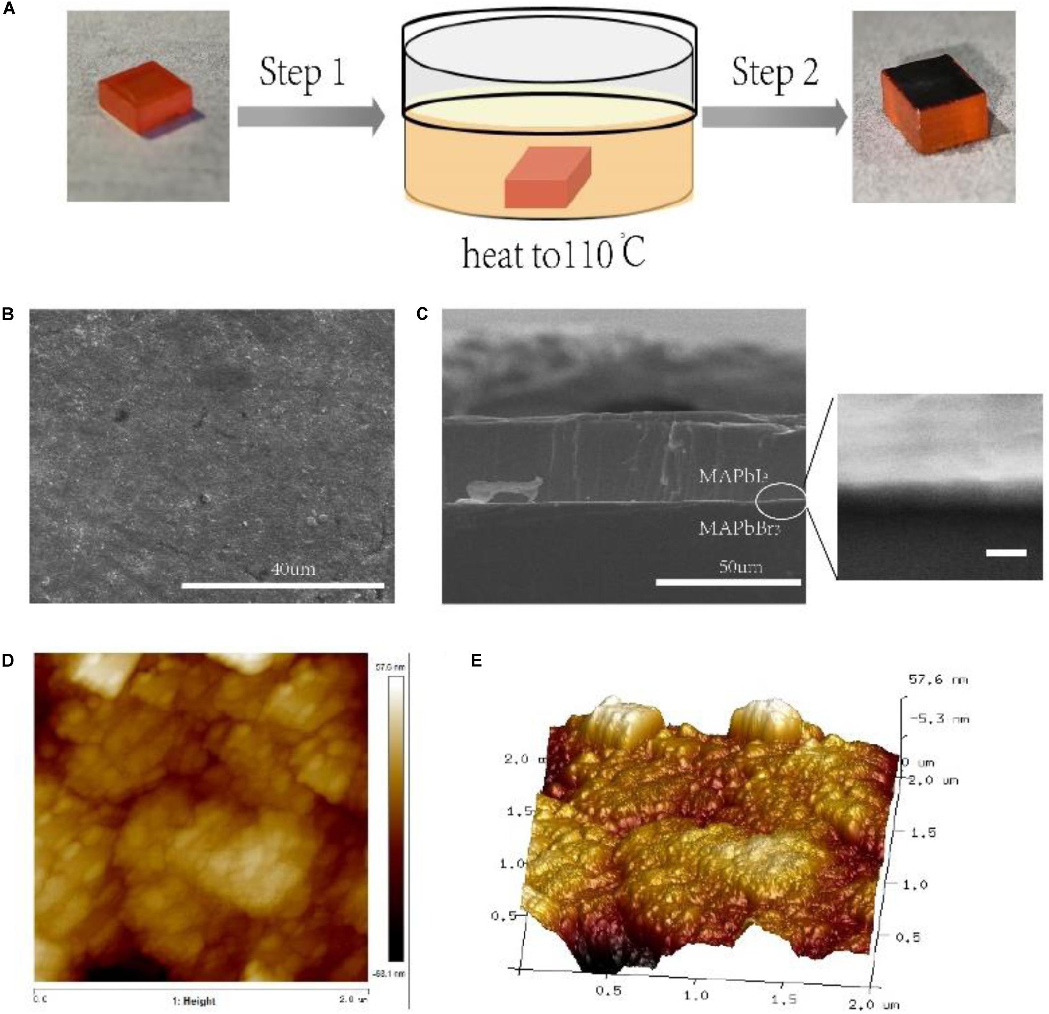
Figure 1. (A) Processing of epitaxial growth of MAPbI3 SCF via solution-process epitaxy. Step 1: put substrate into precursor solution of MAPbI3. Step 2: Cutting and polishing. (B) SEM image of the epitaxial MAPbI3 SCF surface. (C) SEM image of the cross section of the epitaxial MAPbI3 SCF on MAPbBr3 single crystal substrate. The small figure is SEM image of the interface of the epitaxial layer and substrate with 1 μm scale. (D) Atomic force microscope (AFM) image of the surface of MAPbI3 film. (E) 3D image of the surface of MAPbI3 film.
XRD and PL characterization are performed to determine the quality and crystallinity of the epitaxial MAPbI3 SCFs. For comparison, the XRD spectra of the epitaxial MAPbI3 on MAPbBr3 (orange line), MAPbBr3 PSC (green line) and MAPbI3 PSC (blue line) are shown, respectively, in Figure 2A. Different from MAPbI3 single crystal of hexagonal structure, the epitaxial MAPbI3 film changes to cubic structure because of the cubic MAPbBr3 substrate (Wang et al., 2019b). Additionally, Figure 2B shows a clear MAPbI3 (200) peak at a Bragg angle of 2θ = 28.22° and a MAPbBr3 (200) peak at 2θ = 28.47°. Furthermore, MAPbI3 (200) peak with a full width at half-maximum (FWHM) of 0.0925 in Figure 2B, which is comparable to MAPbI3 single crystal (200) peak with a FWHM of 0.1121, indicates the high crystallinity of epitaxial MAPbI3 SCFs (Liu et al., 1991, 2016). Figure 2C demonstrates the steady-state PL spectra at room temperature with a strong emission peak at 791 nm under the 450 nm excitation with a FWHM of 32.3 nm, which is smaller than 60 nm of MAPbI3 single crystal and 55 nm of MAPbI3 polycrystalline film (Han et al., 2018), confirming the high quality of epitaxial film.
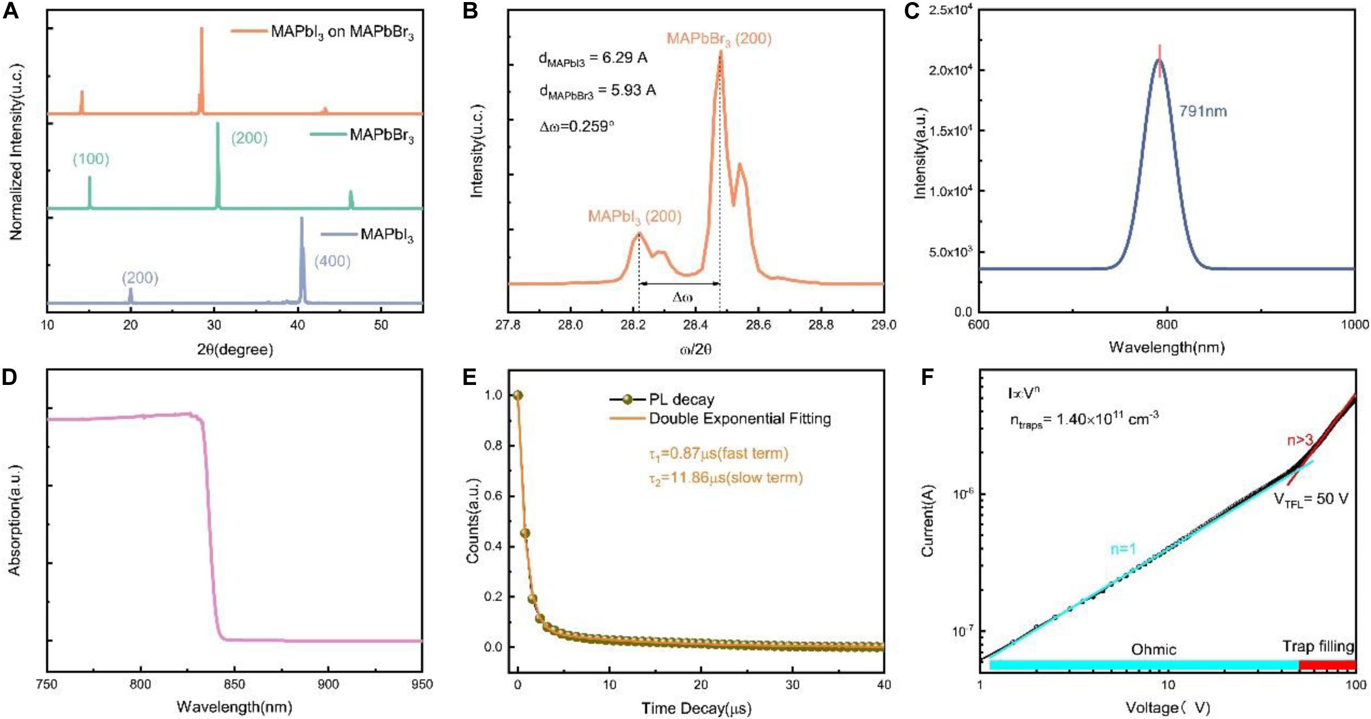
Figure 2. (A) XRD spectra of the epitaxial MAPbI3 SCF on MAPbBr3, MAPbBr3 PSC, and MAPbI3 PSC. (B) XRD spectra of the epitaxial MAPbI3 SCF on MAPbBr3 at Bragg angle from 27.8° to 29.0°. (C) Photoluminescence (PL) spectra of the epitaxial MAPbI3 SCF on MAPbBr3 at room temperature. The PL excitation wavelength is 450 nm. (D) Absorption spectra of the epitaxial MAPbI3 SCF. (E) Time-resolved PL spectra of MAPbI3 SCF on MAPbBr3 at the peak emission wavelength of 791 nm. (F) Current-voltage curve for the epitaxial MAPbI3 based structure.
Moreover, Figure 2D illustrates that the absorption onset of epitaxial MAPbI3 SCF is 840 nm, which are comparable to the 850 nm absorption onset of MAPbI3 single crystal (Dong et al., 2015). And the redshift is obvious compared to the 780 nm absorption onset of polycrystalline MAPbI3 film (Zhang et al., 2016). As shown in Figure 2E, double exponential fitting is performed to evaluate the carrier lifetime (τ) of epitaxial MAPbI3 SCF. The short lifetime of 0.874 ±0.002 μs indicates surface recombination while long lifetime of 11.86 ±0.14 μs suggests bulk recombination (Shi et al., 2015). The carrier lifetime of epitaxial MAPbI3 SCF is much longer than the carrier lifetime of polycrystalline film of nanosecond scale (Tong et al., 2017). In addition, space-charge-limited current (SCLC) technique is used to estimate the trap density of epitaxial MAPbI3 SCF (Rose, 1955). The formula is , where ε is relative dielectric constant, VTFL is the trap-filled limit voltage, q is the electronic charge. As to the horizontal device architecture in this work, L is the channel length between two gold electrodes, which were deposited on the surface of MAPbI3 films by a shadow mask. As shown in Figure 2F, there is a linear current-voltage curve (n = 1) obeying Ohm’s law since the injected charge carriers at low applied voltage is too weak to completely fill trap center. As the applied voltage gradually increases, the injected carrier concentration is greater than the thermally excited carrier concentration and the conduction law changes from the ohmic mode to the SCLC mode. When the applied voltage further increases, all injected charge carriers are used to fill deep traps and all traps will be filled at VTFL (Quah and Cheong, 2013a,b). Figure 2F exhibits the current-voltage curve for the epitaxial MAPbI3 based structure. The L is 500 μm with 1% error and VTFL is 50 V so that the low trap density is calculated as 5.64(±0.12) × 1011 cm–3, which is much lower than polycrystalline films (Dong et al., 2015; Li et al., 2018). The high quality and crystallinity of epitaxial MAPbI3 SCF benefit the wider absorption range, longer carrier lifetime and lower trap density than polycrystalline films.
To further validate the quality of the epitaxial MAPbI3 SCF, a horizontal architecture photodetector with two golden electrodes deposited on the surface of epitaxial MAPbI3 SCF is fabricated as shown in Figure 3A. A light-emitting diode at 670 nm is used as light source for characterization of optoelectronic performance. Figures 3B,C plot the typical I-V curve under various light illumination intensities and the temporal response at different voltage bias of our photodetector, respectively. The dark current is very low of 7.1 nA at 0.2 V, which benefits the high photocurrent to dark current ratio (ION/IOFF) of 331.7 with 2.5 mW cm–2 light illumination. Additionally, responsivity () and detectivity () are calculated to evaluate the performance of this photodetector (Gong et al., 2009; Zhang et al., 2018). As shown in Figure 3D, R is as high as 1.38 A W–1 and the maximum D is 3.07 × 10¹² jones at 20 V bias with 90 μW cm–2 illumination at 670 nm, which are higher than polycrystalline films-based devices, reflecting the efficiency and ability of this photodetector responds to weak optical signal (Jiao et al., 2017; Wang et al., 2019c). Additionally, responsivities as a function of wavelength from 400 to 900 nm are illustrated in Figure 3E. And the normalized EQE of MAPbBr3 single crystal in Figure 3E indicates that photodetectors based on epitaxial films can widen the absorption range of substrate. As shown in Figure 3F, a 6 ns pulsed laser is used to measure the response speed and it takes only 2.21 μs for current decay to 63% at 20 V bias, which is much faster than devices based on polycrystalline films, owing to the high quality of epitaxial MAPbI3 SCF (Horvath et al., 2014; Mi et al., 2017; Wu et al., 2020).
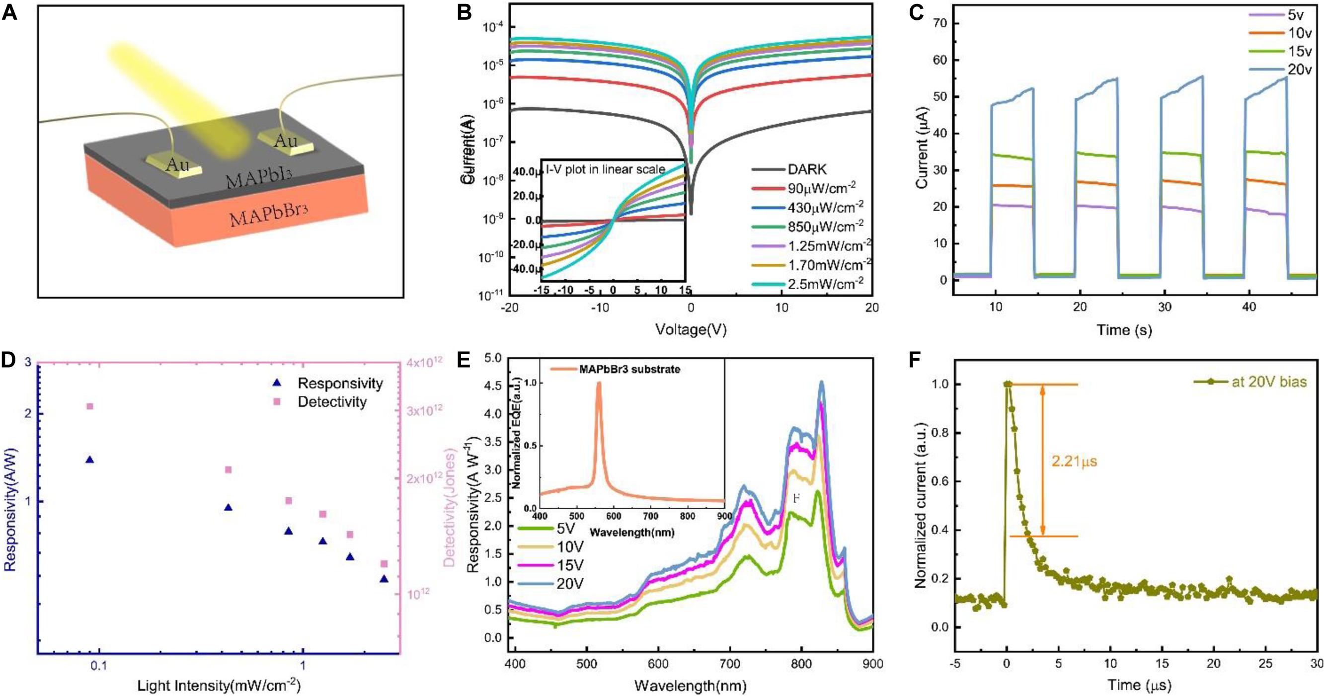
Figure 3. (A) Schematic illustration of our photodetector and the incident light. The size of the photodetector is 0.025 cm2. (B) I-V curves of our photodetector under dark and various light illumination intensities from 90 μW cm–2 to 2.5 mW cm–2. The wavelength of incident light is 670 nm. (C) Temporal response of the photodetector at different voltage bias at 670 nm under 90 μW cm–2 light illumination intensity. (D) Plots of responsivity and detectivity of our photodetector at 20 V bias as a function of light intensity at 670 nm. (E) Responsivity at various incident light wavelength from 400 to 900 nm under different voltage bias and the normalized External Quantum Efficiency (EQE) of MAPbBr3 single crystal. (F) Response time at 20 V bias under a 6 ns pulsed laser.
To further indicate the high quality of epitaxial MAPbI3 SCF, variable temperature crystallization (VTC) method (Wang et al., 2017) is employed for synthesis of MAPbI3 PSC and a photodetector based on MAPbI3 PSC is fabricated and tested under same test environment for comparison in this work. Figures 4A,B illustrate the dark current and the photocurrent with 90 μW cm–2 illumination at 670 nm of epitaxial film-based device and PSC-based photodetector. Epitaxial film-based device has lower dark currents at voltages from 0.2 to 10.4 V bias and higher photocurrents than PSC-based photodetector. As shown in Figure 4C, the ION/IOFF ratios of epitaxial film-based device are about 10 times higher than those of PSC-based photodetector. Figure 4D shows the dark current densities at 20 V bias after various days, which of 25.3 μA cm–2 on day 0 and of 33.11 μA cm–2 on day 120. In addition, Figure 4E shows the long-term stable response of our device on day 120 at 20 V bias. The increasing rate formula is , where Jm and Jn are the dark current densities on day m and day n. The calculated rate of change in dark current density is about 0.255% per day. The good morphology and crystallinity of epitaxial films benefit better stability than polycrystalline films (Salim et al., 2015; Tailor et al., 2020). The comparison of photoelectric performance between different MAPbI3-based devices is shown in Table 1. The excellent performance actually validates the high-quality of the epitaxial MAPbI3 SCFs.
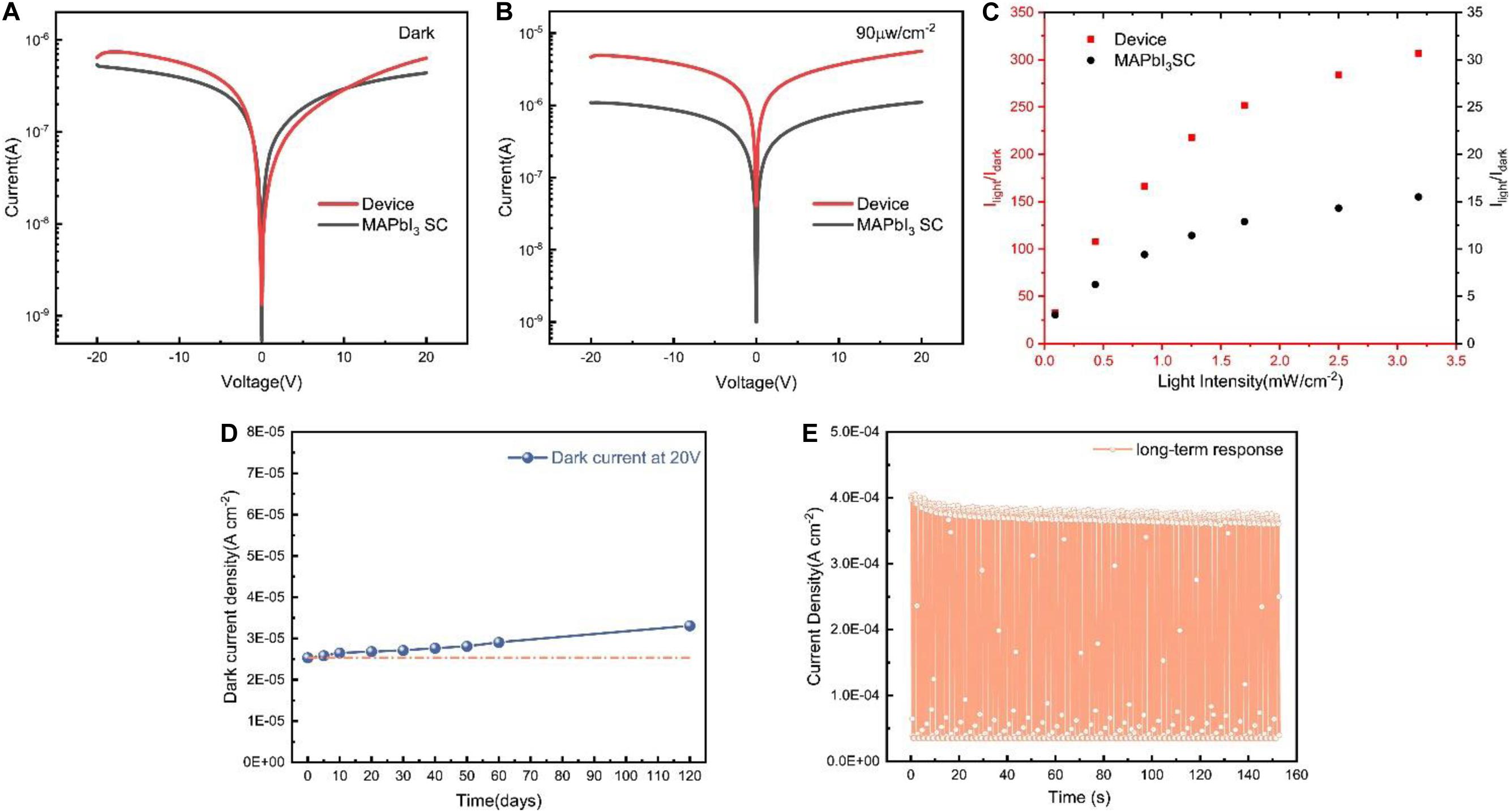
Figure 4. (A) Dark current of our photodetector and MAPbI3 PSC-based photodetector under different voltage bias. (B) Photocurrent of our photodetector and MAPbI3 PSC-based photodetector at 670 nm under 90 μW cm–2 light illumination intensity. (C) ION/IOFF current ratios of our photodetector and MAPbI3 PSC-based photodetector at 20 V bias under various light illumination intensity from 90 μW cm–2 to 3.2 mW cm–2. (D) Long-term dark current density test at 20 V bias. (E) Long-term response of devices after 120 days with a 0.5 Hz LED at 670 nm of 90 μW cm–2 as light source.
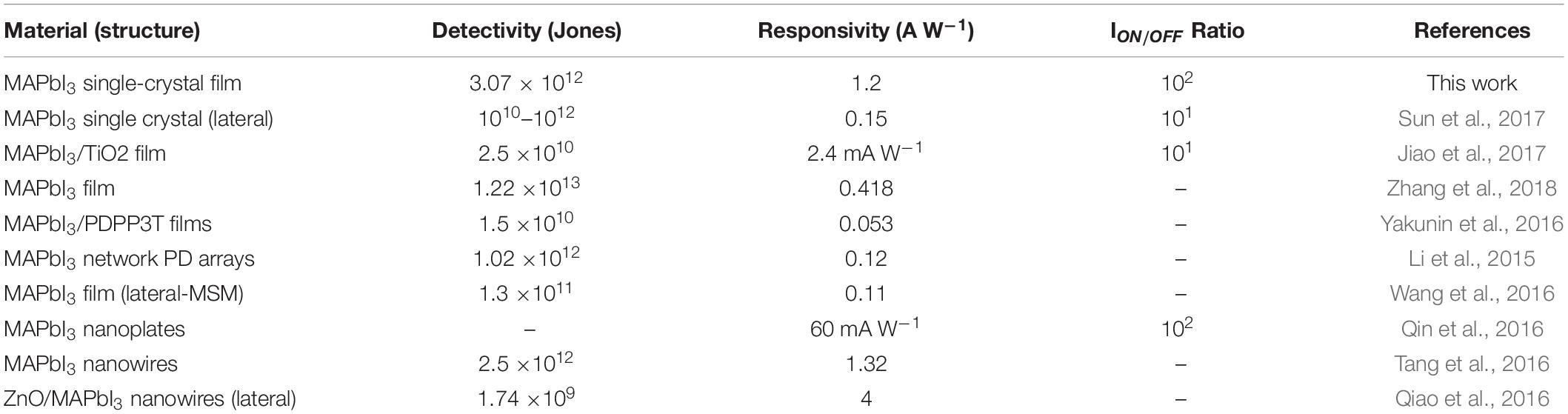
Table 1. Device performance comparison between MAPbI3-based photodetectors.
In summary, this work demonstrates the epitaxial growth of high-quality MAPbI3 single-crystal film on MAPbBr3 substrate with good lattice matching. XRD, AFM, and SEM characterizations are performed to confirm the high crystalline and smooth morphology, which result in the low trap density of 5.64 ×1011 cm–3 and long carrier lifetime of 11.86 μs. Additionally, we fabricate a high-performance photodetector based on epitaxial MAPbI3 SCF with responsivity of 1.2 A W–1, detectivity of 3.07 ×10¹² jones, response time of 2.21 μs and excellent stability for 120 days. Therefore, this epitaxial growth method provides a new path for high-stability perovskite film-based devices.
The raw data supporting the conclusions of this article will be made available by the authors, without undue reservation, to any qualified researcher.
YX, JZ, and YL grew the perovskite single crystals. YX and JZ did the epitaxial experiments. YX, YP, and JZ did the measurements. XW and YX analyzed these results. YX wrote the manuscript. All authors made comments on this manuscript.
This work was financially supported by the National Key Research and Development Program of China (2018YFE0125500, 2016YFB0401600), the Program 111_2.0 in China (BP0719013), the National Natural Science Foundation Project of China (61775034, 51879042, 61674029, 12005038), the Research Fund for International Young Scientists (62050410350), the International Cooperative Research Project of Jiangsu Province (BZ2018056), and the Leading Technology of Jiangsu Basic Research Plan (BK20192003).
The authors declare that the research was conducted in the absence of any commercial or financial relationships that could be construed as a potential conflict of interest.
Abdi-Jalebi, M., Pazoki, M., Philippe, B., Dar, M. I., Alsari, M., Sadhanala, A., et al. (2018). Dedoping of Lead Halide Perovskites Incorporating Monovalent Cations. ACS Nano 12, 7301–7311. doi: 10.1021/acsnano.8b03586
Chen, Y., Lei, Y., Li, Y., Yu, Y., Cai, J., Chiu, M. H., et al. (2020). Strain engineering and epitaxial stabilization of halide perovskites. Nature 577, 209–215.
Chen, Y., Peng, J., Su, D., Chen, X., and Liang, Z. (2015). Efficient and balanced charge transport revealed in planar perovskite solar cells. ACS Appl. Mater. Interfaces 7, 4471–4475. doi: 10.1021/acsami.5b00077
Cho, H. C., Jeong, S. H., Park, M. H., Kim, Y. H., Wolf, C., Lee, C. L., et al. (2015). Overcoming the electroluminescence efficiency limitations of perovskite light-emitting diodes. Science 350, 1222–1225. doi: 10.1126/science.aad1818
Dong, Q., Fang, Y., Shao, Y., Mulligan, P., Qiu, J., Cao, L., et al. (2015). Electron-hole diffusion lengths & 175 μm in solution-grown CH3NH3PbI3 single crystals. Science 347, 967–970.
Fang, Y., Dong, Q., Shao, Y., Yuan, Y., and Huang, J. (2015). Highly narrowband perovskite single-crystal photodetectors enabled by surface-charge recombination. Nat. Photonics 9, 679–686. doi: 10.1038/nphoton.2015.156
Fei, C., Li, B., Zhang, R., Fu, H., Tian, J., and Cao, G. (2017). Highly efficient and stable perovskite solar cells based on monolithically grained CH3NH3PbI3 film. Adv. Energy Mater. 7:1602017. doi: 10.1002/aenm.201602017
Gong, X., Tong, M., Xia, Y., Cai, W., Moon, J. S., Cao, Y., et al. (2009). High-detectivity polymer photodetectors with spectral response from 300 nm to 1450 nm. Science 325, 1665–1667.
Han, C., Wei, Z., Wang, K., Yu, H., Deng, L., Zhu, X., et al. (2018). Effect of surface recombination in high performance white-light CH3NH3PbI3 single crystal photodetectors. Opt. Express 26, 26307–26316. doi: 10.1364/oe.26.026307
Horvath, E., Spina, M., Szekrenyes, Z., Kamaras, K., Gaal, R., Gachet, D., et al. (2014). Nanowires of methylammonium lead iodide (CH3NH3PbI3) prepared by low temperature solution-mediated crystallization. Nano Lett. 14, 6761–6766. doi: 10.1021/nl5020684
Hou, Y., Wu, C., Huang, X., Yang, D., Ye, T., Yoon, J., et al. (2020). Self−powered Red/UV narrowband photodetector by unbalanced charge carrier transport strategy. Adv. Funct. Mater. 31:2007016. doi: 10.1002/adfm.202007016
Ji, L., Hsu, H. Y., Lee, J. C., Bard, A. J., and Yu, E. T. (2018). High-performance photodetectors based on solution-processed epitaxial grown hybrid halide perovskites. Nano Lett. 18, 994–1000.
Jiang, S., Wang, X., Wu, Y., Li, Y., Zhang, Q., Li, G., et al. (2019). Balance lead in solution-processed CH3NH3PbBrxCl(3-x) single crystals for high performance X-ray detection. Mater. Lett. 236, 26–29. doi: 10.1016/j.matlet.2018.10.055
Jiao, S., Fu, X., Lian, G., Jing, L., Xu, Z., Wang, Q., et al. (2017). Ultrathin TiO2nanosheets synthesized using a high pressure solvothermal method and the enhanced photoresponse performance of CH3NH3PbI3–TiO2composite films. RSC Adv. 7, 20845–20850. doi: 10.1039/c7ra01073g
Kelso, M. V., Mahenderkar, N. K., Chen, Q., Tubbesing, J. Z., and Switzer, J. A. (2019). Spin coating epitaxial films. Science 364, 166–169.
Kim, Y. C., Kim, K. H., Son, D. Y., Jeong, D. N., Seo, J. Y., Choi, Y. S., et al. (2017). Printable organometallic perovskite enables large-area, low-dose X-ray imaging. Nature 550, 87–91. doi: 10.1038/nature24032
Li, F., Ma, C., Wang, H., Hu, W., Yu, W., Sheikh, A. D., et al. (2015). Ambipolar solution-processed hybrid perovskite phototransistors. Nat. Commun. 6:8238.
Li, Y., Li, Y., Shi, J., Zhang, H., Wu, J., Li, D., et al. (2018). High quality perovskite crystals for efficient film photodetectors induced by hydrolytic insulating oxide substrates. Adv. Funct. Mater. 28:1705220. doi: 10.1002/adfm.201705220
Li, Y.-W., Wang, X., Li, G.-W., Wu, Y., Pan, Y.-Z., Xu, Y.-B., et al. (2020). Fast liquid phase epitaxial growth for perovskite single crystals∗. Chin. Phys. Lett. 37:018101. doi: 10.1088/0256-307x/37/1/018101
Ling, Y., Yuan, Z., Tian, Y., Wang, X., Wang, J. C., Xin, Y., et al. (2016). Bright light-emitting diodes based on organometal halide perovskite nanoplatelets. Adv. Mater. 28, 305–311. doi: 10.1002/adma.201503954
Liu, S., Lu, Y.-J., Kappes, M. M., and Ibers, J. A. (1991). The structure of the C60 molecule: x-ray crystal structure determination of a twin at 110 K. Science 254, 408–410. doi: 10.1126/science.254.5030.408
Liu, Y., Zhang, Y., Yang, Z., Yang, D., Ren, X., Pang, L., et al. (2016). Thinness- and shape-controlled growth for ultrathin single-crystalline perovskite wafers for mass production of superior photoelectronic devices. Adv. Mater. 28, 9204–9209. doi: 10.1002/adma.201601995
Long, G., Jiang, C., Sabatini, R., Yang, Z., Wei, M., Quan, L. N., et al. (2018). Spin control in reduced-dimensional chiral perovskites. Nat. Photonics 12, 528–533.
Mi, B., Li, H., Song, Z., Zhao, G., Tong, G., and Jiang, Y. (2017). Hybrid perovskite photoconductivity visible region detector with high speed and stability. Nano 12:1750150. doi: 10.1142/s1793292017501508
Pan, Y., Wang, X., Xu, Y., Li, Y., Elemike, E. E., Shuja, A., et al. (2020). Enhanced performance of perovskite single-crystal photodiodes by epitaxial hole blocking layer. Front. Chem. 8:791. doi: 10.3389/fchem.2020.00791
Qiao, K., Deng, H., Yang, X., Dong, D., Li, M., Hu, L., et al. (2016). Spectra-selective PbS quantum dot infrared photodetectors. Nanoscale 8, 7137–7143. doi: 10.1039/c5nr09069e
Qin, X., Yao, Y., Dong, H., Zhen, Y., Jiang, L., and Hu, W. (2016). Perovskite Photodetectors based on CH3NH3PbI3 single crystals. Chem. Asian J. 11, 2675–2679.
Quah, H. J., and Cheong, K. Y. (2013a). Current conduction mechanisms of RF-Magnetron sputtered Y2O3 gate oxide on gallium nitride. Curr. Appl. Phys. 13, 1433–1439. doi: 10.1016/j.cap.2013.04.028
Quah, H. J., and Cheong, K. Y. (2013b). Surface passivation of gallium nitride by ultrathin RF-magnetron sputtered Al2O3 gate. ACS Appl. Mater. Interfaces 5, 6860–6863. doi: 10.1021/am402333t
Rose, A. (1955). Space-charge-limited currents in solids. Phys. Rev. 97:1538. doi: 10.1103/physrev.97.1538
Salim, T., Sun, S., Abe, Y., Krishna, A., Grimsdale, A. C., and Lam, Y. M. (2015). Perovskite-based solar cells: impact of morphology and device architecture on device performance. J. Mater. Chem. A 3, 8943–8969. doi: 10.1039/c4ta05226a
Shao, Y., Xiao, Z., Bi, C., Yuan, Y., and Huang, J. (2014). Origin and elimination of photocurrent hysteresis by fullerene passivation in CH3NH3PbI3 planar heterojunction solar cells. Nat. Commun. 5:5784.
Shi, D., Adinolfi, V., Comin, R., Yuan, M., Alarousu, E., Buin, A., et al. (2015). Low trap-state density and long carrier diffusion in organolead trihalide perovskite single crystals. Science 347, 519–522. doi: 10.1126/science.aaa2725
Stranks, S. D., and Snaith, H. J. (2015). Metal-halide perovskites for photovoltaic and light-emitting devices. Nat. Nanotechnol. 10, 391–402. doi: 10.1038/nnano.2015.90
Sun, H., Lei, T., Tian, W., Cao, F., Xiong, J., and Li, L. (2017). Self-powered, flexible, and solution-processable perovskite photodetector based on low-cost carbon cloth. Small 13:1701042. doi: 10.1002/smll.201701042
Tailor, N. K., Abdi-Jalebi, M., Gupta, V., Hu, H., Dar, M. I., Li, G., et al. (2020). Recent progress in morphology optimization in perovskite solar cell. J. Mater. Chem. A 8, 21356–21386. doi: 10.1039/d0ta00143k
Tan, Z. K., Moghaddam, R. S., Lai, M. L., Docampo, P., Higler, R., Deschler, F., et al. (2014). Bright light-emitting diodes based on organometal halide perovskite. Nat. Nanotechnol. 9, 687–692.
Tang, F., Chen, Q., Chen, L., Ye, F., Cai, J., and Chen, L. (2016). Mixture interlayer for high performance organic-inorganic perovskite photodetectors. Appl. Phys. Lett. 109:123301. doi: 10.1063/1.4963269
Tang, G., You, P., Tai, Q., Yang, A., Cao, J., Zheng, F., et al. (2019). Solution-phase epitaxial growth of perovskite films on 2D material flakes for high-performance solar cells. Adv. Mater. 31:e1807689.
Tong, S., Sun, J., Wang, C., Huang, Y., Zhang, C., Shen, J., et al. (2017). High-performance broadband perovskite photodetectors based on CH3NH3PbI3/C8BTBT heterojunction. Adv. Electron. Mater. 3:1700058. doi: 10.1002/aelm.201700058
Wang, J., Xiao, S., Qian, W., Zhang, K., Yu, J., Xu, X., et al. (2021). Self-driven perovskite narrowband photodetectors with tunable spectral responses. Adv. Mater. 33:e2005557.
Wang, Q., Shao, Y., Dong, Q., Xiao, Z., Yuan, Y., and Huang, J. (2014). Large fill-factor bilayer iodine perovskite solar cells fabricated by a low-temperature solution-process. Energy Environ. Sci. 7, 2359–2365. doi: 10.1039/c4ee00233d
Wang, W., Zhang, F., Bai, H., Li, L., Gao, M., Zhanga, M., et al. (2016). Photomultiplication photodetectors with P3HT: fullerene-free material as the active layers exhibiting a broad response. Nanoscale 8, 5578–5586. doi: 10.1039/c6nr00079g
Wang, X., Huang, Y., Lei, W., Li, Q., Zhang, X., Khan, Q., et al. (2017). Asymmetrical photodetection response of methylammonium lead bromide perovskite single crystal. Cryst. Res. Technol. 52:1700115. doi: 10.1002/crat.201700115
Wang, X., Li, Y., Xu, Y., Pan, Y., Zhu, C., Zhu, D., et al. (2020). Solution-processed halide perovskite single crystals with intrinsic compositional gradients for x-ray detection. Chem. Mater. 32, 4973–4983. doi: 10.1021/acs.chemmater.9b05000
Wang, X., Wu, Y., Li, G., Li, Y., Wu, J., Zhang, X., et al. (2019a). Fabrication of photodiodes based on solution-processed perovskite single crystals. IEEE Trans. Electron Devices 66, 485–490. doi: 10.1109/ted.2018.2878828
Wang, X., Wu, Y., Li, G., Wu, J., Zhang, X., Li, Q., et al. (2018). Ultrafast ionizing radiation detection by p–n junctions made with single crystals of solution−processed perovskite. Adv. Electronic Mater. 4:1800237. doi: 10.1002/aelm.201800237
Wang, X. D., Li, W. G., Liao, J. F., and Kuang, D. B. (2019b). Recent advances in halide perovskite single−crystal films: fabrication methods and optoelectronic applications. Solar RRL 3:1800294. doi: 10.1002/solr.201800294
Wang, Y., Shi, Y., Xin, G., Lian, J., and Shi, J. (2015). Two-dimensional van der Waals epitaxy kinetics in a three-dimensional perovskite halide. Cryst. Growth Des. 15, 4741–4749. doi: 10.1021/acs.cgd.5b00949
Wang, Y., Yang, F., Li, X., Ru, F., Liu, P., Wang, L., et al. (2019c). Epitaxial growth of large−scale orthorhombic CsPbBr3 perovskite films with anisotropic photoresponse property. Adv. Funct. Mater. 29:1904913. doi: 10.1002/adfm.201904913
Wei, H., Desantis, D., Wei, W., Deng, Y., Guo, D., Savenije, T. J., et al. (2017). Dopant compensation in alloyed CH3NH3PbBr3-xClx perovskite single crystals for gamma-ray spectroscopy. Nat. Mater. 16, 826–833. doi: 10.1038/nmat4927
Wu, H., Chu, B., and Su, Z. (2020). Improved performance of perovskite photodetectors with a hybrid planar-mixed heterojunction. Mater. Res. Exp. 7:066201. doi: 10.1088/2053-1591/ab98c9
Xing, G., Mathews, N., Lim, S. S., Yantara, N., Liu, X., Sabba, D., et al. (2014). Low-temperature solution-processed wavelength-tunable perovskites for lasing. Nat. Mater. 13, 476–480. doi: 10.1038/nmat3911
Xu, Y., Wang, X., Pan, Y., Li, Y., Emeka Elemike, E., Li, Q., et al. (2020). Perovskite photodetectors based on p-i-n junction with epitaxial electron-blocking layers. Front. Chem. 8:811. doi: 10.3389/fchem.2020.00811
Yakunin, S., Dirin, D. N., Shynkarenko, Y., Morad, V., Cherniukh, I., Nazarenko, O., et al. (2016). Detection of gamma photons using solution-grown single crystals of hybrid lead halide perovskites. Nat. Photonics 10, 585–589. doi: 10.1038/nphoton.2016.139
Yang, D., Yang, Z., Qin, W., Zhang, Y., Liu, S., and Li, C. (2015). Alternating precursor layer deposition for highly stable perovskite films towards efficient solar cells using vacuum deposition. J. Mater. Chem. A 3, 9401–9405.
Yang, M., Zeng, Y., Li, Z., Kim, D. H., Jiang, C. S., Van De Lagemaat, J., et al. (2017). Do grain boundaries dominate non-radiative recombination in CH3NH3PbI3 perovskite films? Phys. Chem. Chem. Phys. 19, 5043–5050.
Zhang, F., Song, J., Zhang, L., Niu, F., Hao, Y., Zeng, P., et al. (2016). Film-through large perovskite grains formation via a combination of sequential thermal and solvent treatment. J. Mater. Chem. A 4, 8554–8561.
Keywords: perovskite, epitaxial growth, photodetector, solution-processed, single-crystal film
Citation: Xu Y, Wang X, Zhao J, Pan Y, Li Y, Elemike EE, Li Q, Zhang X, Chen J, Zhao Z, Akram J, Bae BS, Bin S and Lei W (2021) Solution-Processed Epitaxial Growth of MAPbI3 Single-Crystal Films for Highly Stable Photodetectors. Front. Mater. 8:651957. doi: 10.3389/fmats.2021.651957
Received: 11 January 2021; Accepted: 22 March 2021;
Published: 09 April 2021.
Edited by:
Fabian Ifeanyichukwu Ezema, University of Nigeria, Nsukka, NigeriaReviewed by:
Hock Jin Quah, University of Science Malaysia, MalaysiaCopyright © 2021 Xu, Wang, Zhao, Pan, Li, Elemike, Li, Zhang, Chen, Zhao, Akram, Bae, Bin and Lei. This is an open-access article distributed under the terms of the Creative Commons Attribution License (CC BY). The use, distribution or reproduction in other forums is permitted, provided the original author(s) and the copyright owner(s) are credited and that the original publication in this journal is cited, in accordance with accepted academic practice. No use, distribution or reproduction is permitted which does not comply with these terms.
*Correspondence: Xin Wang, MjMwMTU5NDI0QHNldS5lZHUuY24=; Wei Lei, bHdAc2V1LmVkdS5jbg==
Disclaimer: All claims expressed in this article are solely those of the authors and do not necessarily represent those of their affiliated organizations, or those of the publisher, the editors and the reviewers. Any product that may be evaluated in this article or claim that may be made by its manufacturer is not guaranteed or endorsed by the publisher.
Research integrity at Frontiers
Learn more about the work of our research integrity team to safeguard the quality of each article we publish.