
95% of researchers rate our articles as excellent or good
Learn more about the work of our research integrity team to safeguard the quality of each article we publish.
Find out more
ORIGINAL RESEARCH article
Front. Mater. , 19 August 2015
Sec. Mechanics of Materials
Volume 2 - 2015 | https://doi.org/10.3389/fmats.2015.00056
This article is part of the Research Topic New Frontiers in Multiscale Modelling of Advanced Materials View all 16 articles
The distributed plasticity of pentatwinned silver nanowires has been revealed in recent computational and experimental studies. However, the molecular dynamics (MD) simulations have not considered the imperfections seen in experiments, such as irregular surface undulations, the high aspect ratio of nanowires, and the stiffness of loading devices. In this work, we report the effect of such inherent imperfections on the distributed plasticity of penta-twinned silver nanowires in MD simulations. We find that the distributed plasticity occurs for nanowires having undulations that are less than 5% of the nanowire diameter. The elastic stress field induced by a stacking fault promotes the nucleation of successive stacking fault decahedrons (SFDs) at long distance, making it hard for necking to occur. By comparing the tensile simulation using the steered molecular dynamics method with the tensile simulation with periodic boundary condition (PBC), we show that a sufficiently long nanowire must be used in the constant strain rate simulations with PBC, because the plastic displacement burst caused by the SFD formation induces compressive stress, promoting the removal of other SFDs. Our finding can serve as a guidance for the MD simulation of crystalline materials with large plastic deformation and in the design of mechanically reliable devices based on silver nanowires.
Silver nanowires have been widely used as building blocks in various electronic systems including flexible antennas (Song et al., 2014), highly stretchable strain sensors (Liu and Choi, 2009; Amjadi et al., 2014), transparent conductive films, and flexible conductors (Xu and Zhu, 2012) due to their high conductivity and ease of synthesis (Zhang et al., 2005). Most of those applications are expected to sustain cyclic mechanical loading and be used as components in wearable and flexible devices. For example, silver nanowire–elastomer composite based piezoresistivity sensors experience complex cyclic mechanical loading during their operation (Amjadi et al., 2014) and the nanowire-based touch screen has also been tested under large bending and stretching (Xu and Zhu, 2012). The conductivity of these devices is provided by a percolation network made of silver nanowires and their failure highly depends on the integrity of the network. Therefore, for the reliable design of flexible devices, it is essential to understand the mechanical integrity of the silver nanowire under high strain beyond the plastic limit as well as its recovery under unloading.
In addition, there is a fundamental interest in understanding the plasticity of silver nanowires, for two reasons. First, silver nanowires have a unique penta-twinned structure when chemically synthesized (Zhang et al., 2005; Liu and Choi, 2009; Xu and Zhu, 2012; Amjadi et al., 2014; Song et al., 2014). Nanostructures incorporating nanotwins have been extensively studied with the goal of simultaneously improving their strength and ductility. Second, it is known that the plasticity of a sub-100 nm metal specimen is driven by dislocation nucleation, and thus is very different from bulk counterparts, in which plastic deformation is governed by the motion of existing dislocations. Penta-twinned nanowires can serve as a simple test bed for studying both the role of twin boundaries (TBs) (Zhu and Gao, 2012) and the size effect, together. For example, a few novel properties of penta-twinned nanowires have been revealed including enhance elastic modulus (Zhu et al., 2012), enhanced yield strength (Wu et al., 2006), special multiple conjoint fivefold twins (Jiang et al., 2013a,b), and thermal effects originated from the size effect and the TBs (Wu et al., 2011).
Numerous computational and experimental studies have been devoted to examining the plasticity of penta-twinned nanowires (Cao and Wei, 2006; Wu et al., 2011; Filleter et al., 2012; Sun et al., 2013; Zheng et al., 2014). It was found that the yield of the nanowire initiates with dislocation nucleation from the surface, and plastic deformation is accommodated by a chain of stacking fault decahedrons (SFD) or stacking fault hats (SFH). Multiple distributed plastic zones have been observed for sub-100 nm nanowires, and their mechanism has been explained by the activation and deactivation of SFD chains at stress concentrations due to a surface undulation. Recently, a recoverable plasticity has also been reported by two independent studies (Bernal et al., 2014; Qin et al., 2015) suggesting the crucial role of TBs in blocking the propagation of stacking faults and promoting the recovery under unloading.
However, molecular dynamics (MD) simulation studies have not considered the irregular surface undulation, the high aspect ratio of nanowires, and the stiffness of loading devices that are inherent in experiments. While stress concentrations associated with the irregular surface undulation have been suggested as the origin of distributed plastic zones, there has been no MD simulation that tests the assumptions. The large plastic displacement burst induced by the formation of the SFD chain may significantly affect the stress–strain relationship if nanowires with small aspect ratio are tested in MD simulations. Also, the constant strain rate simulation with a periodic boundary condition (PBC) is equivalent to the use of an infinite stiffness loading device, which may result in a deformation mechanism that is different from the experiments.
In this work, we employ MD simulations to study the effect of the aforementioned factors in the deformation behaviors. We found that the distributed plasticity occurs for nanowires with undulations that are less than 5% of the nanowire diameter. The elastic stress field induced by a stacking fault promotes the delocalization of SFDs, making it hard for necking to occur. For higher diameter undulation, the stress concentration is too high to accommodate a separate plastic zone at a different stress-concentration position. By comparing the tensile simulation using the steered molecular dynamics (SMD) method with the tensile simulation with PBC, we show that a sufficiently long nanowire must be used in the constant strain rate simulations with PBC, because the plastic displacement burst caused by the SFD formation induces compressive stress, which promotes the removal of other SFHs or SFDs.
We employed LAMMPS (Plimpton, 1995) and MD++ (MD++; http://micro.stanford.edu/MDpp) MD packages to study the mechanical behavior of penta-twinned silver nanowires. The interactions between atoms were described by embedded-atom-method (EAM) potential. We tested two versions of EAM potentials developed by Sheng et al. (2011) and Williams et al. (2006). The diameter of the nanowires was around 20 nm, and two different aspect ratios (6 and 12) were considered. The penta-twinned nanowire has a <110 > direction along the growth axis and five single face-centered-cubic (FCC) crystals intersect at the {111} TBs (Figure 1). To mimic the surface defects and diameter variation observed in experiments (Filleter et al., 2012; Bernal et al., 2014), the nanowire has surface undulations along the axial direction (Agrawal et al., 2009) as shown in Figure 1B. At each cross section of the undulation site, we considered an imaginary circle of identical size but centered at a shifted position, and atoms above the circle are removed. The magnitude of shift is a sinusoidal function of the axial position with maximum being 5% of nanowire diameter. We did not observe significant re-arrangements on the undulation sites because there is no sharp surface step. The undulation sites are equally spaced in all nanowires considered in this study. The total number of atoms is about two million for the nanowire with the aspect ratio 6 and four million for the aspect ratio 12. Before the tension, the nanowires are equilibrated at 300 K by utilizing NPT ensemble for 600 ps and NVT ensemble for 600 ps until long period vibration modes decay. Time step and damping parameters are chosen as 1 fs and 0.1, respectively. The average length of nanowire during the NPT equilibration is used as the reference length for computing engineering strain.
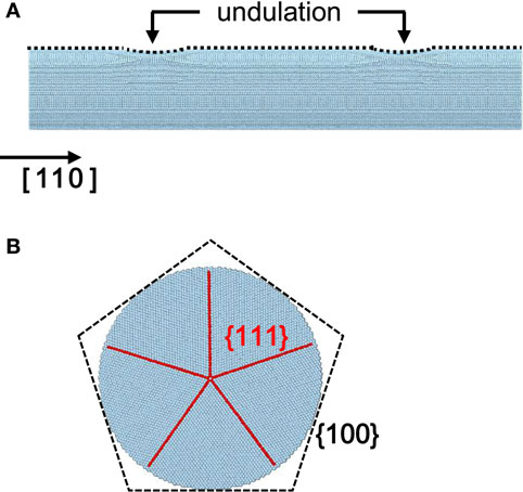
Figure 1. (A) The configuration of the silver nanowire with aspect ratio 6 in perspective view. The black line is the twin boundaries. The two black arrows indicate the sinusoidal shaped undulation. (B) The circular cross section of the penta-twinned nanowire.
The tensile loading was performed with two methods. One is the conventional tensile simulation where the simulation box is expanded with a constant rate under PBC. The other is the SMD method where one end of the nanowire is pulled by an imaginary spring while the other end is fixed. For both simulations, we used the time step of 1 fs. The tensile loading simulation of the conventional method was performed at 300 K under canonical ensemble (NVT) with an engineering strain rate of 0.1 ns−1 until fracture occurred. We increase the size of the simulation cell in the loading direction every 10 ps with a fixed strain increment (0.001) and run NVT simulations for 10 ps until it reaches equilibrium. We then measured the average stress, and repeated the elongation and NVT simulation sequence multiple times. The virial stress formula was used to calculate the atomic stress of the nanowires (Pendás, 2002; Zimmerman et al., 2004).
For the SMD method, one end of nanowire is fixed and the other end of nanowire is pulled by a virtual spring. On the onset of plasticity, a large plastic strain burst occurs that cannot be captured by the conventional PBC method. Due to the compliance of the virtual spring, the SMD method is suitable for capturing the large strain while it cannot apply a perfect displacement control. When performing SMD method, we chose the spring constant to be comparable to the stiffness of the 120 nm-long nanowires, and the pulling speed of the spring was chosen to achieve the engineering strain rate of 0.1 ns−1. During SMD simulation, the temperature was kept at 300 K using identical thermostats. To analyze the dislocation structure in the plastic zone, we visualized the dislocation lines with different colors according to their category using OVITO (Alexander, 2010) and Crystal Analysis (Alexander and Karsten, 2010) packages.
First, we compare the deformation behavior of two nanowires with and without diameter undulation (~5% of diameter), as described by the Sheng potential. For the pristine nanowire, the plastic zone is initiated at a random point and extends for a long distance by forming SFD chains, as depicted in Figure 2A. In contrast, the deformation of the nanowire with the undulation is accommodated by two distinct plastic zones, activated around the stress concentrated regions, which is similar to the distributed plasticity observed in experiments (Filleter et al., 2012; Bernal et al., 2014) (Figure 2B).
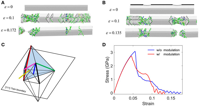
Figure 2. An array of snapshots of (A) a pristine nanowire and (B) a nanowire with undulations at different strains. The PBC method was used to simulate the nanowires with the same potential developed by Sheng et al. Atoms with high central symmetry values are selectively visualized, and the line color indicates the type of dislocations. (C) Double Thompson tetrahedron painted with different colors by categorizing Burgers vector: red, perfect dislocation with 1/2 <110 >a; black, through twin partial with 1/9 <222 >a; blue, stair-rod dislocation with 1/6 <110 >a; purple, Frank partial with 1/3 <111 >a; yellow, Hirth partial with 1/3 <001 >a; green, Shockley partial with 1/6 <112 >a. The color coding is the same in the dislocation line of MD snapshots. (D) Stress–strain curve obtained from tensile simulations of two nanowires.
Interestingly, for the nanowire with undulations, the plastic zone extends for a large distance before necking occurs, as it does in the pristine nanowire. We found that the toughness moduli, evaluated by integrating the stress–strain curve from zero to fracture strain, are almost identical for the two cases (Figure 2D), which indicates that the nanowire accommodates a large plastic deformation despite the presence of stress concentration. Due to this tendency to develop a non-localized plastic zone, the penta-twinned nanowire is tolerant to small surface undulations and can absorb a large amount of energy until failure. This may explain why highly stretchable sensors or touch screens based on the nanowire percolation network can sustain significant cyclic loadings (Xu and Zhu, 2012; Amjadi et al., 2014; Narayanan et al., 2014; Yang et al., 2014; Wang et al., 2015). To analyze the dislocation structures, we drew a double Thompson tetrahedron to visualize the Burgers vector of dislocation of the FCC structure (Figure 2C). The most predominant dislocation is the Shockley partial with the Burgers vector 1/6 <112 >a (the lines painted green color in the Figure) which represents the leading and trailing part of the stacking fault planes in the SFD chains. The next dominant partial dislocation with Burgers vector 1/9 <222 >a (black color in figure) is formed at the intersection between the stacking fault and the TB (Bernal et al., 2014).
To probe whether the observed behavior was independent of the empirical potential choice as well as the small aspect ratio, we compared the tensile simulations of nanowires having four undulation sites with larger aspect ratio (12), using both Sheng and Mishin potentials (Figures 3A–C). The different results from the potentials are originated from different choices of fitting properties (Williams et al., 2006; Sheng et al., 2011). Still, regardless of the potential type, we observed the activation of a distinct plastic zone around the undulation sites, and found that some of SFD chains remained until the fracture took place, although the amount of plastic deformation was different between the two potential models.
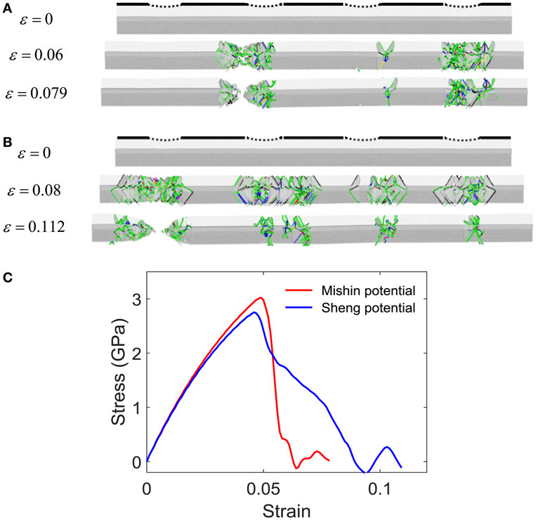
Figure 3. An array of snapshots of AgNWs with different potentials, (A) Mishin and (B) Sheng with the aspect ratio of 12. (C) The stress–strain curves of AgNWs which have the same aspect ratio (12) and different EAM potential. The PBC method was applied to obtain the snapshots and stress–strain curves.
Nevertheless, the MD simulations indicated that the distributed plasticity is an intrinsic property of the penta-twinned nanowire, independent of length, potentials, and the number of surface undulations. Yet, we note that the abrupt reduction of stress following the SFD chain formation has not been observed in tensile tests in experiments (Filleter et al., 2012; Bernal et al., 2014). This may be attributed to the remarkably high strain rate or the much smaller diameter used in simulation. Further research is necessary to clarify this issue.
To understand the origin of the SFD chain formation, we calculated the energy barrier for the formation of a stacking fault plane in the presence of another stacking fault by using the modified nudged elastic band (NEB) methods (Figure 4A) (Ryu et al., 2011). Due to high computational cost, we considered nanowires with smaller diameters (6, 8, 10, and 12 nm). For the diameter of 12 nm, the minimum occurs at a distance of around 3.5 nm (3.31 nm for Sheng potential and 3.61 nm for Mishin potential), as shown in Figure 4C. Also, the energy barrier is significantly smaller than the initial stacking fault nucleation energy barrier in the pristine nanowire at the same stress. This explains why, with smaller diameter, the propagation of SFH chains occurs away from the stress-concentration region. We found that the most probable successive nucleation distance δ between the first SFH and second SFH is linearly proportional to the diameter of the nanowire D (Figure 4B), with the ratio δ ~ 0.28D. This linear relationship implies that the observed energy minimum may be caused by an elastic stress field induced by the first SFH.
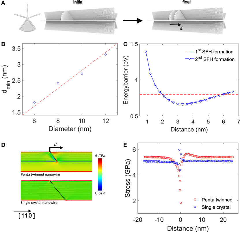
Figure 4. (A) The initial and the final configurations for energy barrier calculations. (B) The distance from the first SFH which makes the optimal value as a function of the diameter of AgNWs. The aspect ratios are the same as 3 and the potential is Sheng. (C) Energy barrier with respect to the distance from the first SFH with Sheng potentials. The diameter of the nanowires is 12 nm and the aspect ratio is 3. (D) The Von-Mises stress fields in the presence of a stacking fault on the (111) plane for penta-twinned and single crystal nanowire having identical diameter and aspect ratio. Mishin EAM potential is used. (E) The Von-Mises stress of atoms which are located at the surface of two types of AgNWs as a function of the distance.
We illustrated the elastic stress field in the nanowire when a single stacking fault presents at 0 K, as shown in Figures 4D,E. The Von-Mises stress of atoms at the surface maximizes around 3 nm, which is close to the most probable nucleation distance δ. Von-Mises stress is calculated from six components of virial stress of each atom, with atomic volume of silver in bulk (10.3 cc/mol) (Wang et al., 1997). We also visualized the Von-Mises stress field of a single crystal nanowire under the same strain (0.04) at 0 K. As shown is Figures 4D,E, the stress field induced from a stacking fault in a single crystal nanowire does not have stress concentration, which clearly shows the role of the TBs in the distributed plasticity of the penta-twinned nanowire. The mismatch between the energy barrier calculation and surface Von-Mises stress plot occurs because the nucleation barrier depends on the integral of the stress field within the dislocation loop at the transition state, not solely on the surface stress. Still, we can conclude that the elastic stress field induced by the stacking fault plane in a penta-twinned nanowire reduces the nucleation barrier of another stacking fault plane, promoting the formation of a long SFH chain, much like a catalytic reaction.
Next, we studied the effect of nanowire length on the deformation behavior. Although the nanowire tested in these experiments was about a few micrometers long, most MD simulations consider a nanowire a few tens of nanometers scale, because of the computational cost (Cao and Wei, 2006; Agrawal et al., 2009; Zheng et al., 2014) with PBC. Nevertheless, that is not enough to fully mimic in simulations the actual experimental conditions. Especially for penta-twinned nanowires, the displacement from a large plastic strain burst is not negligible compared to the nanowire length. For conventional tensile simulations with strain control using PBC, the plastic strain burst in the nanowire induces large stress reduction that effectively causes a significant drop in elastic stress. To overcome the artifacts from the plastic strain burst, we performed the tensile simulation using the SMD method.
We noticed a few differences in deformation behaviors between the two tensile testing methods. First, the extent of the SFH chain after the fracture is much larger in the case of the SMD simulation (Figures 5A,B). The large plastic strain burst from SFH chain formation is accommodated well in the SMD method by length extension. However, the strain burst occurs within a fixed nanowire length in the PBC method and gives rise to internal compressive stress within the nanowire, promoting the removal of SFHs.
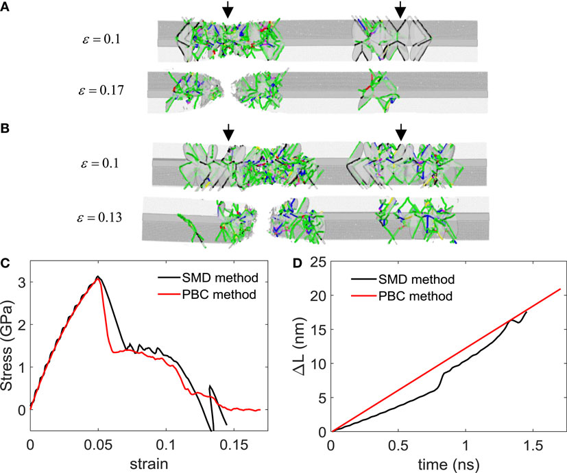
Figure 5. (A) Snapshots of AgNW when the method of simulation is affine deformation by deforming simulation box (PBC method). The black arrows indicate the locations of the undulation sites (B) Snapshots obtained from the SMD method. The potential is the same as Mishin and the configurations of the nanowires are also the same (D = 20 nm, AR = 6). (C) Stress–strain curve with different methods to simulate uni-axial tensile test, and (D) the length increment as a function of time.
The stress–strain curves manifest the differences between the two methods (Figure 5C). A much sharper stress drop is observed after the initial SFH chain nucleation in PBC due to the reduction of elastic tensile stress caused by the plastic strain burst. In contrast, Figure 5D shows that the nanowire length increases abruptly on the verge of plastic deformation under tensile loading by the SMD method. When the nanowires are stretched to the failure strain, the size of the plastic zone remains smaller for the PBC method because a large portion of SFH are removed by the internal compressive stress.
In summary, we studied the distributed plasticity of penta-twinned silver nanowires by performing large scale MD simulations. We observed distributed plasticity when the diameter undulation was <5% for two different empirical potentials. A multiple plastic zone formation was explained by dislocation nucleation from local stress concentrations in the undulated region, which leads to SFH chain propagation. The catalytic formation of the SFH chain is caused by the reduction of the nucleation energy barrier due to the concentrated elastic stress field.
The effects of nanowire length and the loading device stiffness were investigated by comparing two tensile testing methods. We found that the plastic strain burst by the SFH chain induces a moderate compressive stress in the simulation cell, causing excessive removal of SFHs. Such an artifact of simulation can be overcome by employing the SMD method, in which the nanowire can accommodate large plastic strain burst by length extension.
The authors declare that the research was conducted in the absence of any commercial or financial relationship that could be construed as a potential conflict of interest.
This work is supported by Basic Science Research Program (2013R1A1A010091) and Global Frontier Program (No. 2013M3A6B1078881) through the National Research Foundation of Korea (NRF) funded by the Ministry of Science, ICT and Future Planning.
Agrawal, R., Peng, B., and Espinosa, H. D. (2009). Experimental-computational investigation of ZnO nanowires strength and fracture. Nano Lett. 9, 4177–4183. doi: 10.1021/nl9023885
Alexander, S. (2010). Visualization and analysis of atomistic simulation data with OVITO-the open visualization tool. Model. Simul. Mater. Sci. Eng. 18, 015012. doi:10.1088/0965-0393/18/1/015012
Alexander, S., and Karsten, A. (2010). Extracting dislocations and non-dislocation crystal defects from atomistic simulation data. Model. Simul. Mater. Sci. Eng. 18, 085001. doi:10.1088/0965-0393/18/8/085001
Amjadi, M., Pichitpajongkit, A., Lee, S., Ryu, S., and Park, I. (2014). Highly stretchable and sensitive strain sensor based on silver nanowire-elastomer nanocomposite. ACS Nano 8, 5154–5163. doi:10.1021/nn501204t
Bernal, R. A., Aghaei, A., Lee, S., Ryu, S., Sohn, K., Huang, J., et al. (2014). Intrinsic Bauschinger effect and recoverable plasticity in pentatwinned silver nanowires tested in tension. Nano Lett. 15, 139–146. doi:10.1021/nl503237t
Cao, A., and Wei, Y. (2006). Atomistic simulations of the mechanical behavior of fivefold twinned nanowires. Phys. Rev. B 74, 214108. doi:10.1103/PhysRevB.74.214108
Filleter, T., Ryu, S., Kang, K., Yin, J., Bernal, R. A., Sohn, K., et al. (2012). Nucleation-controlled distributed plasticity in penta-twinned silver nanowires. Small 8, 2986–2993. doi:10.1002/smll.201200522
Jiang, S., Chen, Z., Zhang, H., Zheng, Y., and Li, H. (2013a). Impact-induced bending response of single crystal and five-fold twinned nanowires. Int. J. Multiscale Comput. Eng. 11, 1–16. doi:10.1615/IntJMultCompEng.2012003171
Jiang, S., Shen, Y., Zheng, Y., and Chen, Z. (2013b). Formation of quasi-icosahedral structures with multi-conjoint fivefold deformation twins in fivefold twinned metallic nanowires. Appl. Phys. Lett. 103, 041909. doi:10.1063/1.4816666
Liu, C. X., and Choi, J. W. (2009). An embedded PDMS nanocomposite strain sensor toward biomedical applications. (1557-170X (Print)).
Narayanan, S., Hajzus, J. R., Treacy, C. E., Bockstaller, M. R., and Porter, L. M. (2014). Polymer embedded silver-nanowire network structures – a platform for the facile fabrication of flexible transparent conductors. ECS J. Solid State Sci. Technol. 3, 363–369. doi:10.1149/2.0131411jss
Pendás, A. M. (2002). Stress, virial, and pressure in the theory of atoms in molecules. J. Chem. Phys. 117, 965–979. doi:10.1063/1.1484385
Plimpton, S. (1995). Fast parallel algorithms for short-range molecular dynamics. J. Comput. Phys. 117, 1–19. doi:10.1006/jcph.1995.1039
Qin, Q., Yin, S., Cheng, G., Li, X., Chang, T. H., Richter, G., et al. (2015). Recoverable plasticity in penta-twinned metallic nanowires governed by dislocation nucleation and retraction. Nat. Commun. 6, 5983. doi:10.1038/ncomms6983
Ryu, S., Kang, K., and Cai, W. (2011). Entropic effect on the rate of dislocation nucleation. Proc. Natl. Acad. Sci. U.S.A. 108, 5174–5178. doi:10.1073/pnas.1017171108
Sheng, H. W., Kramer, M. J., Cadien, A., Fujita, T., and Chen, M. W. (2011). Highly optimized embedded-atom-method potentials for fourteen fcc metals. Phys. Rev. B 83, 134118. doi:10.1103/PhysRevB.83.134118
Song, L., Myers, A. C., Adams, J. J., and Zhu, Y. (2014). Stretchable and reversibly deformable radio frequency antennas based on silver nanowires. ACS Appl. Mater. Interfaces 6, 4248–4253. doi:10.1021/am405972e
Sun, M., Cao, R., Xiao, F., and Deng, C. (2013). Surface and interface controlled yielding and plasticity in fivefold twinned Ag nanowires. Comput. Mater. Sci. 79, 289–295. doi:10.1016/j.commatsci.2013.06.021
Wang, D., Lee, J., Holland, K., Bibby, T., Beaudoin, S., and Cale, T. (1997). Von Mises stress in chemical-mechanical polishing processes. J. Electrochem. Soc. 144, 1121–1127. doi:10.1149/1.1837542
Wang, J., Jiu, J., Araki, T., Nogi, M., Sugahara, T., Nagao, S., et al. (2015). Silver nanowire electrodes: conductivity improvement without post-treatment and application in capacitive pressure sensors. Nano Micro Lett. 7, 51–58. doi:10.1007/s40820-014-0018-0
Williams, P. L., Mishin, Y., and Hamilton, J. C. (2006). An embedded-atom potential for the Cu-Ag system. Model. Simul. Mater. Sci. Eng. 14, 817. doi:10.1088/0953-8984/21/8/084213
Wu, B., Heidelberg, A., Boland, J. J., Sader, J. E., Sun, X., and Li, Y. (2006). Microstructure-hardened silver nanowires. Nano Lett. 6, 468–472. doi:10.1021/nl052427f
Wu, J. Y., Nagao, S., He, J. Y., and Zhang, Z. L. (2011). Role of five-fold twin boundary on the enhanced mechanical properties of fcc Fe nanowires. Nano Lett. 11, 5264–5273. doi:10.1021/nl202714n
Xu, F., and Zhu, Y. (2012). Highly conductive and stretchable silver nanowire conductors. Adv. Mater. Weinheim 24, 5117–5122. doi:10.1002/adma.201201886
Yang, M., Chon, M. W., Kim, J. H., Lee, S. H., Jo, J., Yeo, J., et al. (2014). Mechanical and environmental durability of roll-to-roll printed silver nanoparticle film using a rapid laser annealing process for flexible electronics. Microelectron. Reliab. 54, 2871–2880. doi:10.1016/j.microrel.2014.07.004
Zhang, S. H., Jiang, Z. Y., Xie, Z. X., Xu, X., Huang, R. B., and Zheng, L. S. (2005). Growth of silver nanowires from solutions: a cyclic penta-twinned-crystal growth mechanism. J. Phys. Chem. B 109, 9416–9421. doi:10.1021/jp0441036
Zheng, Y. G., Zhao, Y. T., Ye, H. F., Zhang, H. W., and Fu, Y. F. (2014). Atomistic simulation of torsional vibration and plastic deformation of five-fold twinned copper nanowires. Int. J. Comput. Methods 11(Suppl.01), 1344010. doi:10.1142/S0219876213440106
Zhu, T., and Gao, H. (2012). Plastic deformation mechanism in nanotwinned metals: an insight from molecular dynamics and mechanistic modeling. Scr. Mater. 66, 843–848. doi:10.1016/j.scriptamat.2012.01.031
Zhu, Y., Qin, Q., Xu, F., Fan, F., Ding, Y., Zhang, T., et al. (2012). Size effects on elasticity, yielding, and fracture of silver nanowires: in situ experiments. Phys. Rev. B 85, 045443. doi:10.1103/PhysRevB.85.045443
Keywords: molecular dynamics, dislocation, stacking fault decahedrons, distributed plasticity
Citation: Lee S and Ryu S (2015) Molecular dynamics study on the distributed plasticity of penta-twinned silver nanowires. Front. Mater. 2:56. doi: 10.3389/fmats.2015.00056
Received: 15 May 2015; Accepted: 27 July 2015;
Published: 19 August 2015
Edited by:
Federico Bosia, University of Torino, ItalyReviewed by:
Pratyush Tiwary, ETH Zürich, SwitzerlandCopyright: © 2015 Lee and Ryu. This is an open-access article distributed under the terms of the Creative Commons Attribution License (CC BY). The use, distribution or reproduction in other forums is permitted, provided the original author(s) or licensor are credited and that the original publication in this journal is cited, in accordance with accepted academic practice. No use, distribution or reproduction is permitted which does not comply with these terms.
*Correspondence: Seunghwa Ryu, Department of Mechanical Engineering, Korea Advanced Institute of Science and Technology, KAIST Building N7-4, Room 7107, 291 Daehak-ro, Yuseong-gu, Daejeon 305-701, South Korea,cnl1c2hAa2Fpc3QuYWMua3I=
Disclaimer: All claims expressed in this article are solely those of the authors and do not necessarily represent those of their affiliated organizations, or those of the publisher, the editors and the reviewers. Any product that may be evaluated in this article or claim that may be made by its manufacturer is not guaranteed or endorsed by the publisher.
Research integrity at Frontiers

Learn more about the work of our research integrity team to safeguard the quality of each article we publish.