 Petra Granitzer
 Klemens Rumpf
- Institute of Physics, Karl-Franzens-University Graz, Graz, Austria
In this review, the fabrication of porous silicon/magnetic nanocomposite materials and their physical properties are elucidated. Especially, the investigation of the presented systems with respect to their magnetic properties is reported. Furthermore, the influence of the semiconducting matrix on the properties of the nanocomposites is highlighted. The main focus will be put on silicon used as template material. In general, the nanocomposite systems are fabricated in a two-step process, first by anodization of a silicon wafer to achieve porous silicon structures, and second by electrodeposition of a magnetic material into the pores. The morphology of the porous silicon template offers straight pores, grown perpendicular to the wafer surface. The magnetic nanostructures deposited within the pores lead to specific properties of the composite dependent on their size and shape. Due to their mutual arrangement, magnetic coupling between these structures can occur, whereas, coupling between adjacent pores depends on the porous silicon morphology. In the first section, different types of such template/metal systems are reviewed and second an experimental part follows implying the porous silicon formation as well as the subsequent metal deposition process. Third, the magnetic and optical properties of the systems are described. In the fourth chapter, the influence of the semiconducting matrix on these properties is elucidated and finally some prospects and conclusions are addressed.
Introduction
Due to the miniaturization and integration of numerous microelectronic devices, low dimensional structures are under extensive investigation with respect to a simple and low-cost fabrication process but also concerning their specific properties. Beside lithographic bottom-up or top-down procedures, self-assembled arrangements of nanoparticles are also a key-topic in many of today’s research fields. Self-organization of nanoparticles depends strongly on the interactions between them resulting in specific one-, two-, or three-dimensional arrangements. To avoid agglomeration of the particles and to stabilize them in general, they are coated with a surfactant. The kind of surfactant determines the inter-particle interactions and thus influences the resulting assembly. A further possibility of self-organization of particles is template guided. Porous materials are suitable candidates, whereas in most cases, the templates themselves are formed by self-organization. Beside, e.g., trench etched polymers (Chou St et al., 1995), porous alumina (Masuda and Fukuda, 1995; Masuda et al., 1997), and porous InP (Gerngross et al., 2013), porous silicon is a well-known and often-employed material. The pore formation is self-organized, nevertheless the morphology is tunable in a broad range and even quasi-regular arrangements can be achieved (Rumpf et al., 2010a).
Porous silicon, a versatile material, which has been discovered in the mid 1950s (Uhlir, 1956) and has been extensively investigated in the 1990s (Canham, 1990; Lehmann and Gösele, 1991; Koshida and Koyama, 1992; Zhang, 2001), is nowadays still an often-employed material in many research fields. After Canham showed in 1990 that microporous silicon emits light in the visible at room temperature due to quantum confinement, optoelectronic applications have been under intense discussion. The demonstration of electroluminescence by Koshida in 1995 pursued this research direction. Concurrent investigations of this material have been related to the tunable morphology and porosity (Föll et al., 2002; Lehmann, 2002), especially with respect to sensing of various molecules (Sailor, 1997; Buriak, 2006). After Canham found that porous silicon is biocompatible and biodegradable (Canham, 1995), this realm was booming (Anglin et al., 2008; Fernandez-Moure et al., 2014). Due to its tunable morphology (Föll et al., 2002) and high surface area (Buriak, 2006), it is applicable in various fields such as gas-sensors (Boarino et al., 2000), bio-sensors (Gupta et al., 2013), optics (Torres-Costa et al., 2005), and many more. The pore-diameters can be varied among the microporous regime (2–4 nm), mesoporous regime (5–50 nm), and macroporous regime (several tens of micrometers). Also its utilization as template material is of interest, e.g., for the deposition of various metals inside the pores (Fukami et al., 2008; Rumpf et al., 2012a; Gerngross et al., 2013). A further advantage to this material is the formation by self-organization (Kompan, 2003) and therefore expensive and time consuming nanopatterning by lithography can be avoided in many cases.
Magnetic nanostructures attract great attention since many years. They are under investigation for magnetic applications such as high density magnetic storage (Sellmyer and Skomski, 2006; Shin et al., 2012) but also for biomedical applications (Pankhurst et al., 2003; Tartaj et al., 2003). The adjustability in their size, shape, and mutual arrangement is examined especially concerning the magnetic properties. Single domain (Goya et al., 2003) and superparamagnetic (Sinwani et al., 2014) particles are crucial in many realms. Their incorporation in a matrix material to determine the magnetic properties or for stabilization is also widespread. Such nanostructured magnetic materials offer completely different properties compared to their bulk materials. A big advantage of nanostructured materials is the tunability of their magnetic properties due to their size, shape, and mutual arrangement.
To fabricate nanostructures (wires), template-assisted methods are used to achieve three-dimensional arrangements of such nanostructures. Such arrays are investigated to get knowledge about the mutual interactions of the magnetic nanostructures, e.g., dipolar coupling (Vazquez et al., 2004) or magnetization reversal mechanisms (Uhlír et al., 2012). A further key-topic is the combination of nanostructured materials, nanocomposites, which are used to process new materials with unique physical properties (Wen and Krishnan, 2011; Wang and Gu, 2015). The intrinsic material characteristics are modified due to the reduced size or the material composition or due to interactions between the nanostructures. Magnetic semiconductors, which are in general magnetic ion-doped semiconductors, are under intense investigation since the last decade. The main goal of this research is the applicability in spintronics. A drawback of these systems is that so far their functionality at room temperature is limited (Dietl and Ohno, 2014). Nevertheless, there is a lot of progress in the choice of the used materials and thus the anticipation is high.
A further route to combine semiconductors and magnetic materials is the incorporation of magnetic nanostructures within a semiconducting template. This incorporation can occur in different ways, either, e.g., by deposition, infiltration, evaporation, or atomic layer deposition. The deposition can be performed electrochemically (Rumpf et al., 2014) or electroless (Nakamura and Adachi, 2012). For the infiltration of magnetic material into a porous structure, usually ready synthesized magnetic nanoparticles in solution (Granitzer et al., 2010) are used. In the following nanocomposite systems consisting of a porous silicon template with deposited magnetic nanostructures will be addressed. Thereby, the fabrication of the systems and the arising distinct properties will be emphasized.
Self-Organized Porous Templates for Metal Deposition
One attractive and often utilized template especially for the deposition of metal nanostructures is porous alumina (Masuda and Fukuda, 1995; Masuda et al., 1997). The pore-arrangement offers a honey-comb like structure and the pores are quite smooth. The pore-diameter is tunable in a regime from about 20 nm up to a few hundred nanometers. In the last decade, magnetic materials such as Ni, Co, and Fe have been deposited within this kind of templates and the resulting magnetic properties have been investigated intensely (Ramazani et al., 2012; Zhang et al., 2013). Recently, porous InP membranes have been employed for the deposition of magnetic metals whereas the deposition process has been examined by FFT-impedance spectroscopy (Gerngross et al., 2014).
A further self-organized template is porous silicon, which is also used for the deposition of magnetic or non-magnetic metal structures into the pores. Already in the 1990s, metal has been deposited within microporous silicon, on the one hand to improve the electric contact in the case of electroluminescence investigations (Ronkel et al., 1996) and on the other hand to influence the luminescence of the material (Huang, 1996; Herino, 1997). Mesoporous silicon with oriented pores of about 20 nm in diameter and thick pore-walls of about 50 nm has been employed as template for the deposition of Ni-wires, which show a magnetic anisotropy due to their shape (Gusev et al., 1994). Porous silicon formed by self-organization has been used with diameters between 25 and 100 nm and concomitant pore-distances between 60 and 40 nm for filling with different magnetic materials (Granitzer et al., 2012a). Depending on the pore-diameter and the concomitant pore-distance, the pore-arrangements offer more or less regularity. A quasi-regular pore-arrangement can be achieved with pore-diameters between 45 and 100 nm, whereas smaller diameters lead to higher irregularity (Rumpf et al., 2011). A further approach to fabricate regular porous silicon pore-arrangements is the pre-patterning of the silicon substrate by a porous alumina template (Zacharatos et al., 2008, 2009).
Experiments
Formation of Nanostructured Silicon
In general, porous silicon can be fabricated by various procedures, wet and dry etching, or a further possibility is high power laser ablation (Laiho and Pavlov, 1995). One kind of a dry etching process is reactive ion etching (RIE) (Tserepi et al., 2003). These dry etching techniques are used in general to fabricate microporous, luminescent porous silicon, whereat a regular arrangement of the pores is not necessary. The most common techniques are wet etching processes such as anodization, stain etching, or metal assisted etching. In the following, these wet etching techniques are briefly addressed especially because the main advantage of these techniques is the tunable morphology and the fabrication of quasi-regular pore-arrangements by self-organization.
Stain etching is an electroless pore formation technique, which has been already described in 1960 (Turner, 1958) and (Archer, 1960). In this process supplementary to the HF solution, an oxidizing agent such as nitric acid solution is added. A lot of progress concerning the stain etching mechanism has been gained recently by Kolasinski (2010) who explained the self-limiting pore formation process and showed that hole injection into the silicon valence band initiates the etching and it is rate determining in the overall etch process. By using V2O5 as oxidant, Kolasinski and Barclay (2013) explained the stoichiometry of the reaction.
The findings are also important for metal-assisted etching for which metal nanoparticles (Ag, Au, Pd, Pt) are deposited on a silicon surface. This process also works electroless. It is mainly used to fabricate silicon nanowires or macropores. So far, literature deals with models in which holes are produced at the metal/silicon interface but which is inappropriate. An explanation of the pore formation has been recently given by Kolasinski (2014). The metal particles are charged with holes by the oxidizing agent resulting in an electric field, which enables the pore formation by anodization. In contrast to the common anodization process in the case of metal-assisted etching, the anodization is localized to the individual metal particles.
Pore formation by anodic dissolution of a silicon wafer leads to a tunable morphology in a broad range, whereas the pore-diameter, inter-pore spacing, and porosity depend on the kind of doping, doping density, electrolyte composition, and electrolyte concentration as well as on the applied current density (Föll et al., 2002). To achieve straight pores grown perpendicular to the surface with diameters <100 nm, one choice is to use highly n-doped silicon, which is anodized in a 10 wt% hydrofluoric acid solution. The bath temperature is at room temperature and the current density is kept constant at 100 mA/cm2, which means the etching is performed under breakthrough conditions. The resulting pore-diameter is about 60 nm and the concomitant distance between the pores is around 40 nm. Figure 1 shows a top-view scanning electron micrograph (SEM) of a typical porous silicon template.
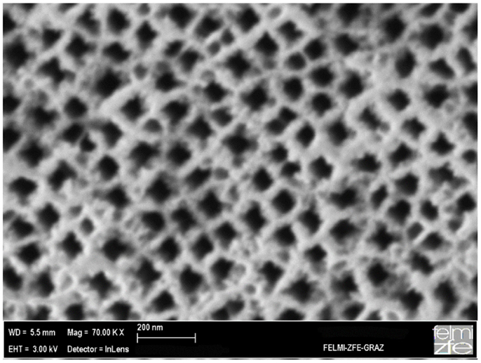
Figure 1. The top-view SEM image of a porous silicon sample shows pores with an average diameter of 60 nm and a mean distance between the pores of 40 nm.
A further parameter of the porous silicon morphology is the dendritic structure of the pores. In the investigated morphology regime, the pores offer such a dendritic growth (Rumpf et al., 2010b). Nevertheless, the occurring branches between adjacent pores are not connected, so the pores are separated from each other. The length of the dendrites increases with decreasing pore-diameter and reaches a maximum of about twice the pore-diameter in the case of small pore-diameters of about 25–30 nm.
To reduce the dendritic structure of the pores, a method developed in the Koshida’ laboratory, magnetic field-assisted etching, has been employed (Hippo et al., 2008). A magnetic field of 8 T applied perpendicular to the sample surface facilitates the directed growth of the pores due to a controlled motion of the holes, which are responsible for the pore formation. As a result, the pore-diameter is decreased and the dendritic pore-growth is drastically reduced.
Such different porous silicon templates are used for filling the pores with a ferromagnetic metal by electrodeposition. The deposition process is performed by a pulsed technique and as electrolyte an adequate metal salt solution is employed. On the one hand, the pulsed technique prevents the exhaustion of the electrolyte and on the other hand blocking of the pores at the pore-opening is avoided. By varying the electrochemical parameters, especially the applied current density and the pulse duration of the current, the shape and size of the deposited nanostructures can be adjusted (Rumpf et al., 2010c). For the deposition of Ni, either the so-called Watts electrolyte (0.2 M NiCl2, 0.1 M NiSO4) or a NiCl2-solution (170 g/l NiCl2) has been used (Rumpf et al., 2010b). For the deposition of Co-nanostructures within the pores, a CoSO4-solution with a pH value of 4.5 has been employed. Considering the pulsed deposition of Ni, a modification of the pulse duration from 40 to 5 s results in an elongation of the deposited structures. By applying 40 s pulses, more or less spherical Ni-particles could be achieved (Figure 2A). A reduction of the pulse duration to 10 s leads to ellipsoidal structures of about 500 nm in length (Figure 2B) and by reducing the pulse duration further to 5 s nanowires up to 4 μm in length could be obtained (Figure 2C). A modification of the applied current density results in a change of the packing density of the deposits.
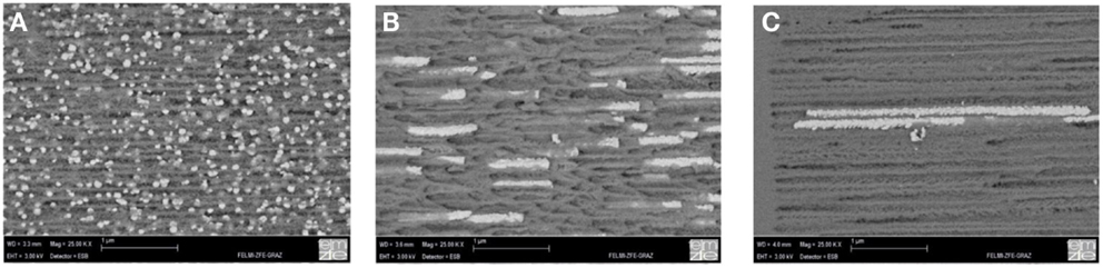
Figure 2. (A) Deposited Ni-particles of about 60 nm in diameter. (B) Ellipsoidal Ni-structures of about 500 nm in length. (C) Ni-wires of about 4 μm in length. The diameter of all structures coincides with the pore-diameter (~60 nm).
In using the equivalent deposition parameters in the case of Co, spherical and ellipsoidal structures with an aspect ratio of about five have been obtained (Rumpf et al., 2012a). The packing density within the pores can be modified similar as in the case of Ni-deposition and thus also the magnetic coupling between the Co-structures can be tuned.
Characterization Methods
For the structural characterization of such nanocomposite systems, the most powerful method is electron microscopy, whereas scanning electron microscopy (SEM) is more appropriate in many cases as transmission electron microscopy (TEM). Images of the cross-section can also be used to estimate the filling factor of the porous silicon template. In this case, it has to be taken into account that SEM not only shows the top surface but also the electrons have a certain depth of penetration dependent on the energy of the primary electrons. In employing TEM, a difficile sample preparation is necessary, which is often a problem in the case of porous structures. Preparation side-effects can effect a slight modification of the pore-structure and also sputtering and re-deposition of silicon has to be considered. A further important feature is the utilization of back-scattered electrons (BSE) to achieve an element sensitive image. Energy dispersive X-ray (EDX) spectroscopy and mapping play a key role to get a survey of the elemental distribution within the pores (Rumpf et al., 2012b).
Fourier transform infrared spectroscopy (FTIR) has been used to figure out the oxidation status of the porous silicon template (Granitzer et al., 2009). Raman-spectroscopy is an appropriate tool to investigate stress caused by the porous silicon formation as well as by the metal filling within the pores (Granitzer et al., 2009).
Magnetic characterization of the samples has been performed by a superconducting quantum interference device (SQUID) and by a vibrating sample magnetometer (VSM). The magnetic field was adjustable between ±6 T in the case of the SQUID and ±9 T in the case of the VSM. The temperature can be varied between 4 and 300 K with both instruments. The magnetization has been measured in two directions, with the magnetic field applied parallel to the pores (easy axis) and perpendicular to the pores (hard axis), respectively.
Magnetic and Optical Properties of the Nanocomposites
Due to the possibility to deposit magnetic nanostructures tunable in their size, shape, and also in their spatial arrangement within the pores, specific magnetic properties can be achieved (Rumpf et al., 2010c). A three-dimensional array of self-assembled ferromagnetic nanostructures renders possible especially to modify the coercivity, remanence, and magnetic anisotropy by tuning the electrochemical parameters and thus the mutual arrangement of the deposited nanostructures. The metal deposits can be modified in their spatial arrangement within the pores by the deposition parameters, especially the applied current density and the pulse duration of the current. A further parameter of modification is the morphology of the template, which allows to vary the wall-thickness and thus the magnetic interactions between nanostructures of adjacent pores. The coercivity increases with decreasing length of the nanostructures and also by decreasing magnetic coupling between metal deposits within adjacent pores (Granitzer et al., 2012b). Figure 3 shows the dependence of the coercivity on the temperature for deposited Ni-wires and Ni-particles within a porous silicon template. The coercivity for deposited particles is always higher than for wires due to demagnetizing effects. Similar results concerning the coercivities and remanence have been reported from metal wires deposited within porous alumina templates (Bahiana et al., 2006).
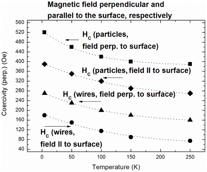
Figure 3. Temperature dependency of coercivities measured in easy axis (magnetic field parallel to the pores) and hard axis (magnetic field parallel to the pores) magnetization, respectively (Rumpf et al., 2012b).
Considering the magnetic properties of Ni-structures dependent on the shape, one sees that the coercivity as well as the remanence increase with decreasing structure–length when dipolar coupling between the deposits can be neglected. In Table 1, a summary of the magnetic properties is given. In the case of elongated metal structures, a magnetic anisotropy between the two magnetization directions, easy axis and hard magnetization occurs. To investigate the crystalline structure of the deposited metal structures, XRD is a suitable tool. It has been reported that Ni-wires within mesoporous silicon are polycrystalline (Dolgiy et al., 2013) and also Co-wires deposited within an InP membrane offer a polycrystalline structure with very small grain size (Gerngross et al., 2014). From our preliminary electron back scatter diffraction (EBSD) experiments, we also found that Ni-deposits within porous silicon are polycrystalline. Due to the fact that the deposits are polycrystalline, the magnetocrystalline anisotropy can be neglected and thus the main anisotropy contribution can be attributed to the shape of the structures.
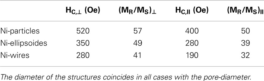
Table 1. Coercivity and remanence in easy axis (magnetic field applied parallel to the pores) and hard axis (magnetic field perpendicular to the pores) magnetization in dependence on the Ni-structure length.
If the distance between the deposited Ni-particles within the pores decreases and a densely packed arrangement is achieved, magnetic coupling between the particles takes place resulting in the magnetic behavior of elongated Ni-structures (quasi-wires). Figure 4 shows cross-sectional images of Ni-particles deposited with a high and a low filling factor, respectively, within porous silicon.
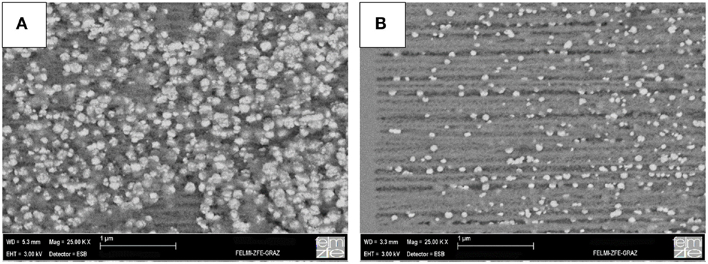
Figure 4. (A) High filling fraction of Ni-particles within porous silicon and (B) low filling density of Ni-particles within the pores. The average particle size is 60 nm.
The values of the coercivity and the remanence for interacting Ni-particles within the pores are comparable with the ones of Ni-wires deposited within porous silicon, HC (easy axis) = 290 Oe, HC (hard axis) = 210 Oe.
Optical methods such as FTIR and Raman-spectroscopy have been used to get knowledge especially about the porous silicon template, its surface, and the interface to the deposited metal structures. By FTIR, the oxidation status of the porous silicon has been figured out and Raman has been used to see if any stress occurs due to the pore formation and the subsequent metal deposition. As etched porous silicon offers a hydrogen terminated surface, which can be seen in FTIR-spectra exhibiting SiH-modes around 2087, 2115, and 2138 cm−1. After aging, the sample in ambient air for 30 min oxide bands around 2250 cm−1 occur, which indicate the formation of a native oxide layer (Granitzer et al., 2009). These results are also confirmed by TEM showing an oxide layer of about 2 nm on the porous silicon wall (Figure 5). After metal deposition within the pores, also oxide bands around 2250 cm−1 appear accompanied by additional peaks around 2964 cm−1, which are due to some SiOx modifications. These additional oxide bands occur during the metal deposition because the reduction of the metal ions is accompanied by an oxidation of the silicon matrix (Sasano et al., 2000).
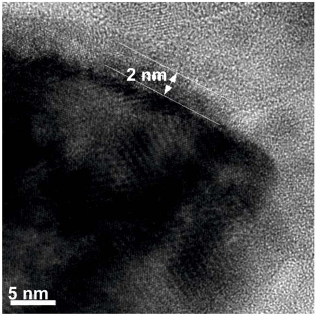
Figure 5. TEM image of an individual porous silicon pore in top view showing the native oxide layer covering the pore-wall (Granitzer et al., 2009).
Raman-spectra show a peak at 522 cm−1 for bare silicon and a slight shift to 520 cm−1 for porous silicon. Ni-deposition within the pores leads to a further shift of the peak to 505 cm−1, which is due to compressive stress and shows the increasing mismatch between bulk silicon and the porous layer (Granitzer et al., 2009). Figure 6 shows the peak shift of the Raman spectra between porous silicon and Ni-filled porous silicon.
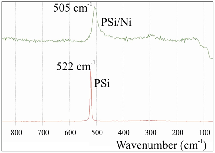
Figure 6. The Raman peak of porous silicon shifts from 522 to 505 cm−1 for porous silicon with Ni filling (Granitzer et al., 2009).
Magneto-optical experiments, investigating the transverse magneto-optical Kerr-effect have been reported on Co deposited within porous silicon (Gan’shina et al., 2005). A correlation among the porosity of the template, the microstructure of the deposited Co, and the magnitude of the Kerr-effect has been found. An enhancement of the magneto-optical response of Ni-nanowires deposited within porous alumina with respect to bulk Ni has been observed (Melles et al., 2003).
Influence of the Template on the Properties of the Nanocomposite
Due to the fact that the pores of the porous silicon templates offer a branched structure (Figure 7), the effective distance between the pores is in the range of 15 nm, which leads to an increase of the magnetic coupling between metal deposits. Concomitant to the porous structure, the metal deposits exhibit the same shape. For these investigations, Ni-wires of a few micrometers in length have been deposited. It could be shown that the magnetic coupling between metal wires of adjacent pores decreases with a decrease of the dendrite-length (Granitzer et al., 2012b). This behavior is accompanied by an increase of the coercivity with decreasing dendritic growth. Also the magnetic anisotropy between easy axis and hard axis magnetization is increased. In Table 2, the coercivities in dependence on the dendrites are presented.
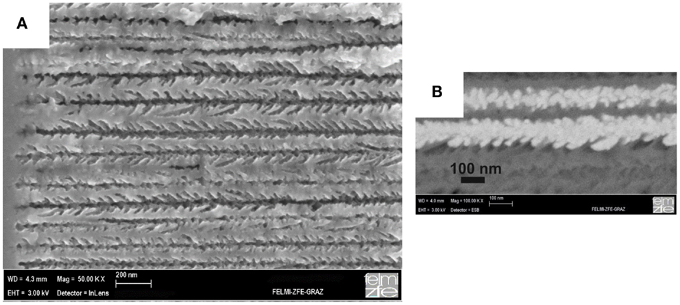
Figure 7. (A) Cross-sectional SEM image of a porous silicon template showing the dendritic pore-growth. (B) BSE-image of Ni-wires deposited within the pores of porous silicon showing their branched structure coinciding with the dendritic pore-growth.
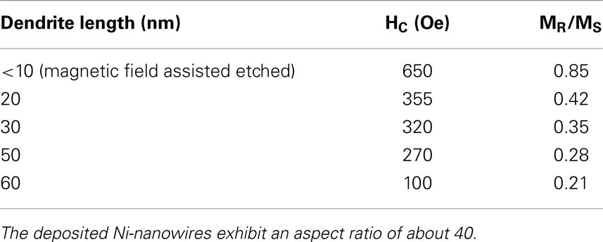
Table 2. Coercivity dependence on the length of the dendrites.
The magnetic behavior of the nanocomposite is strongly influenced by the morphology of the template. As a result of the rough pore-walls, the deposited metal structures exhibit strong stray fields due to their branches, which also diminish the coercivity.
The best results concerning a reduction of the dendritic pore-growth could be achieved by magnetic field assisted etching. Average pore-diameters of about 25 nm with branches below 10 nm could be fabricated and thus also the stray fields effected by the dendrites are reduced, which leads to magnetic properties similar to an isolated nanowire. The decrease of the length of the dendrites has two effects, on the one hand an increase of the effective distance between the pores and on the other hand less magnetic stray fields caused by the branches of the metal deposits. This results in less magnetic coupling between metal structures of adjacent pores and an increase of the magnetization reversal field of the nanowires.
Considering such magnetic nanocomposite systems, one sees that the magnetic properties of the specimens can be tuned in various ways. First, the morphology of the template can be adjusted and thus the magnetic coupling between metal structures of adjacent pores can be tuned. Second, the size and shape of the metal deposits can be tuned, and a third parameter is the filling density and spatial distribution within the pores, which influences the magnetic coupling between deposits within the pores.
Such ferromagnetic/semiconducting composite materials are potential candidates for applications and they are compatible in today’s microtechnology due to the silicon base material. It would be possible to integrate such structures on a chip by using lithography and produce porous silicon selective on localized regions (Hourdakis and Nassiopoulou, 2014).
Perspectives and Conclusion
Self-organized porous systems can be used as template for various materials. The deposition of metals allows to utilize the obtained nanocomposite for numerous applications such as sensor technology, optics, biomedicine, and many more. In incorporating magnetic materials within porous structures, three-dimensional arrays of nanomagnetic structures can be fabricated whereas the magnetic properties are variable through the interaction of the structures and their regularity and morphology of the template. So far, such nanocomposite systems are restricted to basic research but there is a high application potential. In using silicon as template material, the implementation of such nanostructured arrays into today’s microtechnology becomes possible resulting in, e.g., miniaturized magnetic sensors integrated on a chip. Furthermore, the silicon/ferromagnet systems could be utilized in spintronics applications integrated on a chip. In considering spintronics, an advantage of silicon is the rather long spin lifetime, which is due to low spin orbit coupling, zero hyperfine coupling, and degenerate spin states. Furthermore, the spin lifetime in silicon is enhanced, e.g., by reducing electron–phonon scattering processes (Li et al., 2012) or by applying strain, which lengthens the spin coherence time and spin transport length (Tang et al., 2012).
Three-dimensional arrangements of self-organized magnetic nanostructures within a porous template material offer specific magnetic properties, which are tunable by the electrochemical parameters. On the one hand, the size and shape of the deposits can be adjusted by modifying the pulse duration and on the other hand their mutual arrangement within the pores can be varied by changing the current density. The porous silicon template can be used to tune the magnetic interactions between deposits in adjacent pores. Furthermore, the morphology of the template especially the more or less dendritic pore-growth influences the magnetic behavior. A branched pore-structure reduces the effective distance between the pores and therefore increases the magnetic coupling and also gives rise to stray fields and strong demagnetizing fields. In conclusion, one can say that template-assisted assemblies of nanostructures allow to tune the properties of nanocomposites in many ways to achieve desired specimens.
Conflict of Interest Statement
The authors declare that the research was conducted in the absence of any commercial or financial relationships that could be construed as a potential conflict of interest.
Acknowledgments
The authors thank Prof. N. Koshida from the Tokyo University of Agriculture and Technology for the preparation of magnetic field-assisted etched porous silicon samples and the Institute for Electron Microscopy (FELMI) at the University of Technology Graz for electron microscopy, FTIR, and Raman investigations. Furthermore, the authors are grateful for the possibility to perform magnetization measurements at the Institute of Solid State Physics at the Vienna University of Technology.
References
Anglin, E. J., Cheng, L., Freeman, W. R., and Sailor, M. J. (2008). Porous silicon in drug delivery devices and materials. Adv. Drug Deliv. Rev. 60, 1266–1277. doi: 10.1016/j.addr.2008.03.017
Pubmed Abstract | Pubmed Full Text | CrossRef Full Text | Google Scholar
Archer, R. (1960). Stain films on porous silicon. J. Phys. Chem. Solids 14, 104. doi:10.1016/0022-3697(60)90215-8
Bahiana, M., Amaral, F. S., Allende, S., and Altbir, D. (2006). Reversal modes in arrays of interacting magnetic Ni nanowires: Monte Carlo simulations and scaling technique. Phys. Rev. B 74, 174412. doi:10.1103/PhysRevB.74.174412
Boarino, L., Baratto, C., Geobaldo, F., Amato, G., Comini, E., Rossi, A. M., et al. (2000). NO2 monitoring at room temperature by a porous silicon gas sensor. Mater. Sci. Eng. B 6, 210–214. doi:10.1016/S0921-5107(99)00267-6
Buriak, J. M. (2006). High surface area silicon materials: fundamentals and new technology. Phil. Trans. R. Soc. A 364, 217. doi:10.1098/rsta.2005.1681
Pubmed Abstract | Pubmed Full Text | CrossRef Full Text | Google Scholar
Canham, L. T. (1990). Silicon quantum wire array fabrication by electrochemical and chemical dissolution of wafers. Appl. Phys. Lett. 57, 1046–1048. doi:10.1063/1.103561
Canham, L. T. (1995). Bioactive silicon structure fabrication through nanoetching techniques. Adv. Mater. 7, 1033–1037. doi:10.1002/adma.19950071215
Chou St, Y., Krauss, P. R., and Renstrom, P. J. (1995). Imprint of sub 25 nm vias and trenches in polymers. Appl. Phys. Lett. 67, 3114. doi:10.1063/1.114851
Dietl, T., and Ohno, H. (2014). Dilute ferromagnetic semiconductors: physics and spintronic structures. Rev. Mod. Phys. 86, 187. doi:10.1103/RevModPhys.86.187
Pubmed Abstract | Pubmed Full Text | CrossRef Full Text | Google Scholar
Dolgiy, A. L., Redko, S. V., Komissarov, I., Bondarenko, V. P., Yanushkevich, K. I., and Prischepa, S. L. (2013). Structural and magnetic properties of Ni nanowires grown in mesoporous silicon templates. Thin Solid Films 543, 133. doi:10.1016/j.tsf.2013.01.049
Fernandez-Moure, J. S., Evangelopoulos, M., Scaria, S., Martinez, J. O., Brown, B. S., Coronel, A. C., et al. (2014). “Multistage porous silicon for cancer therpy, chapter 16,” in Porous Silicon for Biomedical Applications, ed. H. A. Santos (Cambridge, UK: Woodhead Publishing), 374–402.
Föll, H., Christophersen, M., Carstensen, J., and Hasse, G. (2002). Formation and application of porous silicon. Mater. Sci. Eng. R 39, 93–141. doi:10.1016/S0927-796X(02)00090-6
Fukami, K., Kobayashi, K., Matsumoto, T., Kawamura, Y. L., Sakka, T., and Ogata, Y. H. (2008). Electrodeposition of noble metals into ordered macropores in p-type silicon. J. Electrochem. Soc. 155, D443–D448. doi:10.1149/1.2898714
Gan’shina, E., Yu, A., Kochneva, M., Podgornyi, D. A., Shcherbak, P. N., Demidovich, G. B., et al. (2005). Structure and magneto-optical properties of “porous silicon-cobalt” granular nanocomposites. Phys. Solid State 47, 1383. doi:10.1134/1.1992622
Gerngross, M.-D., Carstensen, J., and Föll, H. (2014). Electrochemical growth of Co nanowires in ultra-high aspect ratio InP membranes: FFT-impedance spectroscopy of the growth process and magnetic properties. Nanoscale Res. Lett. 9, 316. doi:10.1186/1556-276X-9-316
Pubmed Abstract | Pubmed Full Text | CrossRef Full Text | Google Scholar
Gerngross, M.-D., Chemnitz, S., Wagner, B., Carstensen, J., and Föll, H. (2013). Ultra-high aspect ratio Ni nanowires in single-crystalline InP membranes as multiferroic composite. Phys. Status Solidi Rapid Res. Lett. 7, 352. doi:10.1002/pssr.201307026
Goya, G. F., Fonseca, F. C., Jardim, R. F., Muccillo, R., Carreno, N. L. V., Longo, E., et al. (2003). Magnetic dynamics of single-domain Ni nanoparticles. J. Appl. Phys. 93, 6531. doi:10.1063/1.1540032
Granitzer, P., Rumpf, K., Ohta, T., Koshida, N., Poelt, P., and Reissner, M. (2012a). Porous silicon/Ni composites of high coercivity due to magnetic field-assisted etching. Nanoscale Res. Lett. 7, 384. doi:10.1186/1556-276X-7-384
Pubmed Abstract | Pubmed Full Text | CrossRef Full Text | Google Scholar
Granitzer, P., Rumpf, K., Ohta, T., Koshida, N., Reissner, M., and Poelt, P. (2012b). Enhanced magnetic anisotropy of Ni nanowire arrays fabricated on nanostructured silicon templates. Appl. Phys. Lett. 101, 033110. doi:10.1063/1.4738780
Granitzer, P., Rumpf, K., Poelt, P., Albu, M., and Chernev, B. (2009). The interior interfaces of a semiconductor metal nanocomposite and their influence on its physical properties. Phys. State Solid C 6, 2222. doi:10.1002/pssc.200881730
Granitzer, P., Rumpf, K., Venkatesan, M., Roca, A. G., Cabrera, L., Morales, M. P., et al. (2010). Magnetic study of Fe3O4 nanoparticles incorporated within mesoporous silicon. J. Electrochem. Soc. 157, K145–K151. doi:10.1149/1.3425605
Gupta, B., Zhu, Y., Guan, B., Reece, P. J., and Gooding, J. J. (2013). Functionalized porous silicon as a biosensor: emphasis on monitoring cells in vivo and in vitro. Analyst 138, 3593. doi:10.1039/c3an00081h
Pubmed Abstract | Pubmed Full Text | CrossRef Full Text | Google Scholar
Gusev, S. A., Korotkova, N. A., Rozenstein, D. B., and Fraerman, A. A. (1994). Ferromagnetic filaments fabrication in porous Si Matrix. J. Appl. Phys. 76, 6671.
Herino, R. (1997). “Impregnation of porous silicon,” in Properties of Porous Silicon, ed. L. Canham (London: INSPEC), 66–76.
Hippo, D., Nakamine, Y., Urakawa, K., Tsuchiya, Y., Mizuta, H., Koshida, N., et al. (2008). Formation mechanism of 100-nm-scale periodic structures in silicon using magnetic-field-assisted anodization. Jpn. J. Appl. Phys 47, 7398. doi:10.1143/JJAP.47.7398
Hourdakis, E., and Nassiopoulou, A. G. (2014). Single photoresist masking for local porous Si formation. J. Micromech. Microeng. 24, 117002. doi:10.1088/0960-1317/24/11/117002
Huang, Y. M. (1996). Photoluminescence of copper-doped porous silicon. Appl. Phys. Lett. 69, 2855–2857. doi:10.1063/1.117341
Kolasinski, K. W. (2010). Charge transfer and nanostructure formation during electroless etching of silicon. J. Phys. Chem. C 114, 22098. doi:10.1021/jp108169b
Kolasinski, K. W. (2014). The mechanism of galvanic/metal-assisted etching of silicon. Nanoscale Res. Lett. 9, 432. doi:10.1186/1556-276X-9-432
Pubmed Abstract | Pubmed Full Text | CrossRef Full Text | Google Scholar
Kolasinski, K. W., and Barclay, W. B. (2013). The stoichiometry of electroless silicon etching in solutions of V2O5 and HF. Angew. Chem. Int. Ed. 52, 6731. doi:10.1002/anie.201300755
Kompan, M. E. (2003). Mechanism of primary self-organization in porous silicon with regular structure. Phys. Solid State 45, 948. doi:10.1134/1.1575342
Koshida, N., and Koyama, H. (1992). Visible electroluminescence from porous silicon. Appl. Phys. Lett. 60, 347. doi:10.1063/1.106652
Laiho, R., and Pavlov, A. (1995). Preparation of porous silicon films by laser ablation. Thin Solid Films 255, 9. doi:10.1016/0040-6090(94)05621-J
Lehmann, V. (2002). Electrochemistry of Silicon, Instrumentation, Science, Materials and Applications. Weinheim: Wiley-VCH.
Lehmann, V., and Gösele, U. (1991). Porous silicon formation: a quantum wire effect. Appl. Phys. Lett. 58, 856. doi:10.1063/1.104512
Li, J., Qing, L., and Dery, H. I (2012). Appelbaum, field-induced negative differential spin lifetime in silicon. Phys. Rev. Lett. 108, 157201. doi:10.1103/PhysRevLett.108.157201
Pubmed Abstract | Pubmed Full Text | CrossRef Full Text | Google Scholar
Masuda, H., and Fukuda, K. (1995). Ordered metal nanohole arrays made by a two-step replication of honeycomb structures of anodic alumina. Science 268, 1466–1468. doi:10.1126/science.268.5216.1466
Pubmed Abstract | Pubmed Full Text | CrossRef Full Text | Google Scholar
Masuda, H., Hasegawa, F., and Ono, S. (1997). Self-ordering of cell arrangement of anodic porous alumina formed in sulphuric acid solution. J. Electrochem. Soc. 144, L127–L130. doi:10.1149/1.1837634
Melles, S., Menendez, J. L., Armelles, G., Navas, D., Vazquez, M., Nielsch, K., et al. (2003). Magneto-optical properties of nickel nanowires arrays. Appl. Phys. Lett. 83, 4547. doi:10.1063/1.1630840
Nakamura, T., and Adachi, S. (2012). Properties of magnetic nickel/porous silicon composite powders. AIP Adv. 2, 032167. doi:10.1063/1.4754152
Pankhurst, Q. A., Connoly, J., Jones, S. K., and Dobson, J. (2003). Applications of magnetic nanoparticles in biomedicine. J. Phys. D Appl. Phys. 36, R167. doi:10.1088/0022-3727/36/13/201
Ramazani, A., Kashi, M. A., and Seyedi, G. (2012). Crystallinity and magnetic properties of electrodeposited Co nanowires in porous alumina. J. Mag. Mag. Mater. 324, 1826. doi:10.1016/j.jmmm.2012.01.009
Pubmed Abstract | Pubmed Full Text | CrossRef Full Text | Google Scholar
Ronkel, F., Schultze, J. W., and Arens-Fischer, R. (1996). Electrical contact to porous silicon by electrodeposition of iron. Thin Solid Films 276, 40. doi:10.1016/0040-6090(95)08045-7
Rumpf, K., Granitzer, P., Hilscher, G., and Pölt, P. (2011). Interacting low dimensional nanostructures within a porous silicon template. J. Phys. Conf. Ser. 303, 012048. doi:10.1088/1742-6596/303/1/012048
Pubmed Abstract | Pubmed Full Text | CrossRef Full Text | Google Scholar
Rumpf, K., Granitzer, P., Koshida, N., Poelt, P., and Reissner, M. (2014). Magnetic interactions between metal nanostructures within porous silicon. Nanoscale Res. Lett. 9, 412. doi:10.1186/1556-276X-9-412
Pubmed Abstract | Pubmed Full Text | CrossRef Full Text | Google Scholar
Rumpf, K., Granitzer, P., and Pölt, P. (2010a). Influence of the electrochemical process parameters on the magnetic behaviour of a silicon/metal nanocomposite. ECS Trans. 25, 157. doi:10.1149/1.3422509
Rumpf, K., Granitzer, P., and Poelt, P. (2010b). Synthesis and magnetic characterization of metal-filled double-sided porous silicon. Nanoscale Res. Lett. 5, 379. doi:10.1007/s11671-009-9492-6
Pubmed Abstract | Pubmed Full Text | CrossRef Full Text | Google Scholar
Rumpf, K., Granitzer, P., and Pölt, P. (2010c). Formation mechanism of 100-nm-scale periodic structures in silicon using magnetic-field-assisted anodization. ECS Trans. 25, 157. doi:10.1149/1.3422509
Rumpf, K., Granitzer, P., Reissner, M., Poelt, P., and Albu, M. (2012a). Investigation of Ni and Co deposition into porous silicon and the influence of the electrochemical parameters on the physical properties. ECS Trans. 41, 59. doi:10.1149/1.4718391
Rumpf, K., Granitzer, P., Hilscher, G., Albu, M., and Pölt, P. (2012b). Magnetically interacting low-dimensional Ni-nanostructures within porous silicon. Microelectr. Eng. 90, 83. doi:10.1016/j.mee.2011.05.016
Pubmed Abstract | Pubmed Full Text | CrossRef Full Text | Google Scholar
Sailor, M. J. (1997). “Sensor applications of porous silicon,” in Properties of Porous Silicon, ed. L. Canham (London: INSPEC), 364–370.
Sasano, J., Jorne, J., Yoshimi, N., Tsuboi, T., Sakka, T., and Ogata, Y. H. (2000). “Effects of chloride ion on copper deposition into porous silicon,” in Fundamental Aspects of Electrochemical Deposition and Dissolution. Electrochemical Society Proceedings, 84–91.
Sellmyer, D. J., and Skomski, R. (eds) (2006). Advanced Magnetic Nanostructures. New York: Springer.
Shin, J., Goyal, A., Cantoni, C., Sinclair, J. W., and Thompson, J. R. (2012). Self-assembled ferromagnetic cobalt/yttria-stabilized zirconia nanocomposites for ultrohigh density storage applications. Naotechnology 23, 155602. doi:10.1088/0957-4484/23/15/155602
Pubmed Abstract | Pubmed Full Text | CrossRef Full Text | Google Scholar
Sinwani, O., Reiner, J. W., and Klein, L. (2014). Monitoring superparamagnetic Langevin behavior of individual SrRuO3 nanostructures. Phys. Rev. B 89, 020404. doi:10.1103/PhysRevB.89.020404
Tang, J. M., Collins, B. T., and Flatte, M. E. (2012). Electron spin-phonon interaction symmetries and tunable spin relaxation in silicon and germanium. Phys. Rev. B 85, 045202. doi:10.1103/PhysRevB.85.045202
Tartaj, P., Morales, M. P., Veintemillas-Verdaguer, S., Gonzalez-Carreno, T., and Serna, C. J. (2003). The preparation of magnetic nanoparticles for applications in biomedicine. J. Phys. D Appl. Phys. 36, R182. doi:10.1088/0022-3727/36/13/202
Torres-Costa, V., Agullo-Rueda, F., Martin-Palma, R. J., and Martinez-Duart, J. M. (2005). Porous silicon optical devices for sensing applications. Opt. Mater. 27, 1084. doi:10.1016/j.optmat.2004.08.068
Tserepi, A., Tsamis, C., Gogolides, E., and Nassiopoulou, A. G. (2003). Dry etching of porous silicon in high density plasma. Phys. State Solid A 197, 163. doi:10.1002/pssa.200306493
Turner, R. (1958). Electropolishing silicon in hydrofluoric acid solution. J. Electochem. Soc. 105, 402–408. doi:10.1149/1.2428873
Uhlir, A. Jr. (1956). Electrolytic shaping of Germanium and silicon. Bell Syst. Tech. J. 35, 333–347. doi:10.1002/j.1538-7305.1956.tb02385.x
Uhlír, V., Vogel, J., Rougemaille, N., Fruchart, O., Ishaque, Z., Cros, V., et al. (2012). Current-induced domain wall motion and magnetization dynamics in CoFeB/Cu/Co nanostripes. J. Phys. Condens. Matter 24, 024213. doi:10.1088/0953-8984/24/2/024213
Pubmed Abstract | Pubmed Full Text | CrossRef Full Text | Google Scholar
Vazquez, M., Pirota, K., Hernandez-Velez, M., Prida, V. M., Navas, J., Sanz, R., et al. (2004). Magnetic properties of densely packed arrays of Ni nanowires as a function of their diameter and lattice parameter. J. Appl. Phys. 95, 6642. doi:10.1063/1.1687539
Wang, Y., and Gu, H. (2015). Core – shell-type magnetic mesoporous silica nanocomposites for bioimaging and therapeutic agent delivery. Adv. Mater. 27, 576–585. doi:10.1002/adma.201401124
Pubmed Abstract | Pubmed Full Text | CrossRef Full Text | Google Scholar
Wen, T., and Krishnan, K. M. (2011). Cobalt-based magnetic nanocomposites: fabrication, fundamentals and applications. J. Phys. D Appl. Phys. 44, 393001. doi:10.1088/0022-3727/44/39/393001
Zacharatos, F., Gianneta, V., and Nassiopoulou, A. G. (2008). Highly ordered hexagonally arranged nanostructures on silicon through a self-assembled silicon-integrated porous anodic alumina masking layer. Nanotechnology 19, 495306. doi:10.1088/0957-4484/19/49/495306
Pubmed Abstract | Pubmed Full Text | CrossRef Full Text | Google Scholar
Zacharatos, F., Gianneta, V., and Nassiopoulou, A. G. (2009). Highly ordered hexagonally arranged sub-200 nm diameter vertical cylindrical pores on p-type Si using non-lithographic pre-patterning of the Si substrate. Phys. State Solid A Appl. Res. 206, 1286–1289. doi:10.1002/pssa.200881111
Zhang, J. J., Li, Z. Y., Zhang, Z. J., Wu, T. S., and Sun, H. Y. (2013). Optical and magnetic properties of porous anodic alumina/Ni nanocomposite films. J. Appl. Phys. 113, 244305. doi:10.1063/1.4812466
Keywords: nanostructured silicon, magnetic nanostructures, nanocomposite, electrodeposition
Citation: Granitzer P and Rumpf K (2015) Physical properties of semiconducting/magnetic nanocomposites. Front. Mater. 2:4. doi: 10.3389/fmats.2015.00004
Received: 13 November 2014; Accepted: 09 January 2015;
Published online: 28 January 2015.
Edited by:
Samit K. Ray, Indian Institute of Technology Kharagpur, IndiaReviewed by:
Rabah Boukherroub, Centre National de la Recherche Scientifique, FranceKoji Yamada, Nippon Telegraph and Telephone Corporation, Japan
Copyright: © 2015 Granitzer and Rumpf. This is an open-access article distributed under the terms of the Creative Commons Attribution License (CC BY). The use, distribution or reproduction in other forums is permitted, provided the original author(s) or licensor are credited and that the original publication in this journal is cited, in accordance with accepted academic practice. No use, distribution or reproduction is permitted which does not comply with these terms.
*Correspondence: Petra Granitzer, Institute of Physics, Karl-Franzens-University Graz, Universitaetsplatz 5, A-8010 Graz, Austria e-mail:cGV0cmEuZ3Jhbml0emVyQHVuaS1ncmF6LmF0