 Md Tahmid Hussain
 Mohd Tariq
 Adil Sarwar
 Shafiq Ahmad
 Majid Poshtan
 Haitham A. Mahmoud
- 1Department of Electrical Engineering, Zakir Husain College of Engineering and Technology, Aligarh Muslim University, Aligarh, India
- 2Industrial Engineering Department, College of Engineering, King Saud University, Riyadh, Saudi Arabia
- 3Department of Electrical Engineering, Cal Poly State University, San Luis Obispo, CA, United States
This work introduces an 11-level switched-capacitor multilevel inverter (SCMLI) designed for solar photo-voltaic (PV) applications, capitalizing on the growing popularity of multilevel inverters due to their superior power quality. With a 1.67-times boosting capability, the proposed SCMLI employs 10 switches, 2 DC supplies, and 2 capacitors to achieve an 11-level output voltage waveform. The topology requires only seven driver circuits, incorporating 2 bidirectional switches and 3 complementary pairs of switches. The proposed inverter has intrinsic capacitor self-balancing features since the capacitors are connected across the DC voltage source at different times throughout a basic cycle to charge the capacitors at a level of input voltage. A thorough comparison between the topology and recently developed SCMLI’s has been presented. The comparison demonstrates the effectiveness in terms of switches, capacitors, sources, efficiency, total standing voltage (TSV), and boosting capacity. To experimentally validate its performance, the suggested SCMLI undergoes testing using a frequency-based switching method. The topology exhibits low total harmonic distortion (THD) of 7.65% in its output voltage waveform and 0.89% in the output current waveform.
1 Introduction
In the advancement of electric vehicles (EVs), High-Voltage Direct Current (HVDC), renewable energy system, and microgrids technology the multilevel inverters (MLIs) play crucial and prominent role. The MLIs inverter has many distinguishing advantages over two-level inverters, including reduced dv/dt characteristics, improved efficiency, improved EMC, flexibility, and significant fault tolerance capabilities. The requirement for more switches, capacitors, diodes, dc sources, and other components increases under increased voltage stress. However, this significantly increases the size and cost of MLIs. There is a lot of discussion about traditional multilevel converters such as the cascaded H-bridge (CHB), neutral point clamped (NPC), and flying capacitor (FC) (Jayabalan et al., 2017; Khenar et al., 2018). These structures need a lot of components, which makes the system bigger, heavier, and more difficult to regulate. Thus, prompting researchers to look towards structures with a lesser number of components (Gupta et al., 2016; Vemuganti et al., 2021).
Switched-diode, switched-source, and switched-capacitor MLIs (SCMLI) are the three main categories of reduced component structures (RCSs) with the fewest sources and larger boosting capabilities. According to Siddique et al. (2019), the switched-source structure has multiple sources, and the levels in the output voltage are produced by adding their magnitudes algebraically. In Hosseinzadeh et al. (2021), the second arrangement makes use of diodes to link several sources to the load. The third structure also uses capacitors and DC sources. The capacitors are kept at a constant ripple factor and discharge occur during the cycle of operation. The production of the necessary levels in Samadaei et al. (2019) and Iqbal et al. (2020) are achieved by the addition and subtraction of source and capacitor voltages. One method of charging the capacitors is to either connect them in parallel with the source, as shown in Mohamed Ali and Krishnasamy (2019) and Jagabar Sathik et al. (2020), such that the source voltage and the voltage of the capacitor are the same. Utilizing the redundant states of the inverter operation table, as shown in Vahedi et al. (2016) and Sharifzadeh and Al-Haddad (2019), is another option for charging the capacitors. These inverters may be used to integrate rooftop solar photovoltaic (PV) systems for home use into the grid or to power solar-powered irrigation systems (Ali et al., 2021).
Both symmetric and asymmetric RCSs are possible. For higher levels, sources of different magnitudes are often used. For instance, in Chappa et al. (2021), symmetrical sources may provide an output of 9 levels, but asymmetrical ratios of 1:2 and 1:3 can produce outputs of 13 and 17 levels, respectively. Additionally, boosting may be accomplished with a lot of work by using the right sources and/or capacitor combinations (Ye et al., 2021). Ideal MLI should use lesser components and produce higher output voltage levels. The literature discusses capacitors and single-source asymmetrical inverters. The packed U-cell (PUC) inverter, which combines the CHB and FC topologies, is one of the simplest circuits (Ounejjar et al., 2011). The voltage across the capacitor is kept at half of the DC source (Vdc/2) or one-third of the DC source (Vdc/3), respectively, by using one capacitor, six switches, and one source to provide five or seven level output voltage, respectively. To maintain the voltage across the capacitor using the PI controller, a sensor is needed for a 5-level PUC, a sensor-less operation using redundant states was suggested in Vahedi et al. (2016). In Panda et al. (2021), the authors have used twelve switches and a total of five capacitors to develop an 11-level inverter, which employs an auxiliary circuit to handle the intricate control logic. The inventors of Priyadarshi et al. (2020) decreased the number of switches for the same number of levels to 10, but it still needs a lot of capacitors and diodes such as nine capacitors and nine are required. In Tayyab et al. (2022), the authors present an eleven-level inverter with a five-time boost. Although the topology has boosting ability, it has a higher THD and also uses a larger number of driver circuits as compared to the proposed topology. Thus, it increases the requirement for a larger size filter and also increases the overall cost of the inverter. Due to lower THD and fewer driver circuits, the requirement for filter size is reduced, which also makes the topology more cost-effective. For active and reactive power control of grid, the authors present a dual-source, asymmetrical, eleven-level inverter in Tayyab et al. (2023). Even though the topology has a higher efficiency and a lesser number of devices, it also has a higher THD of nearly 12.0%, no boosting capability, and a high minimum required input voltage to operate as compared to the inverter presented in this paper. For energy storage and smart grid applications, a novel switched capacitor multilevel inverter topology with lesser direct current (dc) supply requirement which can operate both in symmetric and asymmetric mode has been presented in Hussan et al. (2020) and a dual-source, cross-connected, asymmetrical 15-level switched-capacitor multilevel inverter novel topology with lesser switch count and number of drivers is presented in Hussan et al. (2021a). An eleven-level inverter topology using two DC sources, eight insulated gate bipolar transistors with antiparallel diodes, two bi-directional power semi-conductor switches, two diodes, and two capacitors is shown in this article.
The remainder of this work is structured as follows. The eleven-level MLI circuit and its functioning are covered in Section 2. Section 3 provides information on the inherent balance of capacitors and capacitance determination. The Nearest Level Control Pulse Width Modulation (NLCPWM) technique is covered in depth in Section 4 to improve the performance of the proposed inverter. The loss analysis of the proposed topology is illustrated in Sections 5. The suggested topology is also contrasted with current 11-level topologies in Section 6. The results were confirmed using MATLAB/SIMULINK and have been affirmed on an experimental setup in Section 7. The application of proposed multilevel inverter in solar PV system is discussed in Section 8. Lastly, Section 9 brings this article to a conclusion.
2 Proposed switched-capacitor topology and analysis
This section discusses the modelling and analysis of proposed 11-level SCMLI. Figure 1A depicts the suggested 11-level inverter topology. The following are the main elements of the proposed MLI: Two bi-directional (S5 and S6) and eight unidirectional switches (S1, S2, S3, S4, S7, S8, S9, and S10), two asymmetrical DC sources in magnitude (V1 = Vdc and V2 = Vdc/2), two diodes, and two capacitors (C1 and C2), which inherently balance at Vdc. Figure 1B shows the 11-level output voltage waveform with a voltage boost of 1.6. The output voltage waveform has a voltage level of 0, ±Vdc/2, ±Vdc, ±3Vdc/2, ±2Vdc, and ±5Vdc/2 across the load. Three complementary switch pairs are included in the suggested topology: S1 and S2, S3 and S4, and S7 and S8. The switches should not be turned on at the same time in order to avoid short-circuit situation.
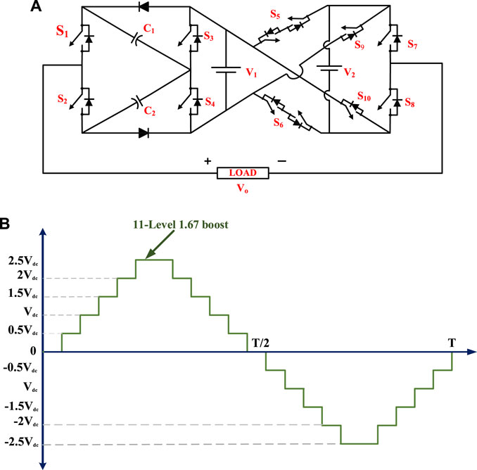
FIGURE 1. (A) Proposed 11-level inverter topology, (B) 11-level output voltage waveform.
2.1 Operation of proposed 11-level topology headings
In this section, the operation of proposed 11-level SCMLI is presented. The conduction patterns for each switching condition are illustrated in Table 1 and Figures 2A–K. The impact of various switching states has been noted for easier understanding of proposed SCMLI. The entries “1” and “0” in Table 1 represents the on and off states of corresponding switches. The letters “CH”, “DCH,” and “NC” stands for the respective capacitors’ charging, discharging, and no change, respectively. The suggested topology voltage levels for the positive half cycle are shown in Figures 2A–F. The conduction route is shown by black lines, and the non-conducting path by grey lines.
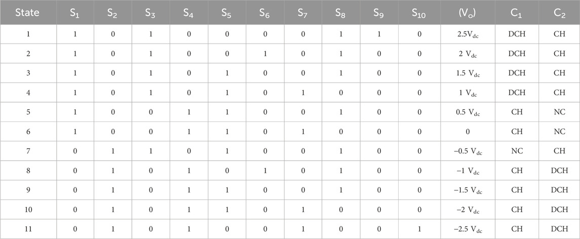
TABLE 1. Switching State for proposed 11-Level SCMLI.
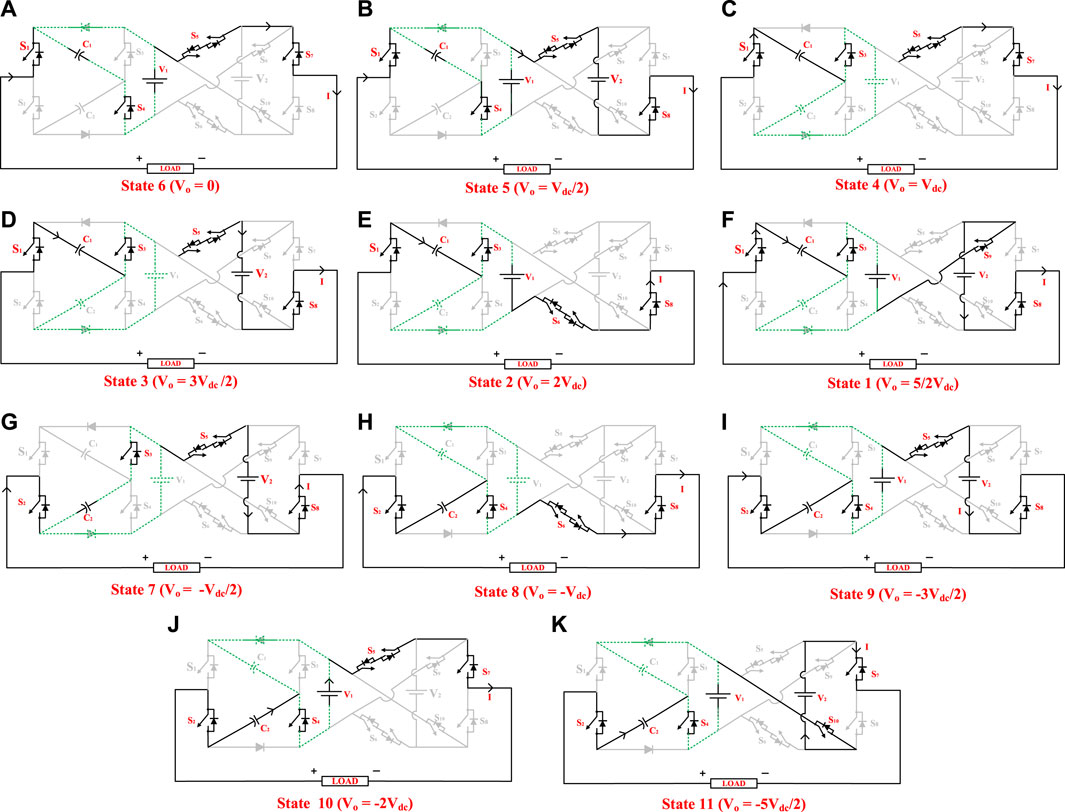
FIGURE 2. Positive and negative half cycle states of proposed 11-level inverter topology: (A) Vo = 0, (B) Vo = 0.5Vdc, (C) Vo = 1Vdc, (D) Vo = 1.5Vdc, (E) Vo = 2Vdc, (F) Vo = 2.5Vdc (G) Vo = −0.5Vdc, (H) Vo = −1Vdc, (I) Vo = −1.5Vdc, (J) Vo = −2Vdc, (K) Vo = −2.5Vdc.
2.2 Working of the topology for different voltage level states
In this section, the working of proposed SCMLI is discussed. The following steps are used to acquire the various positive output voltages:
2.2.1 Zero voltage level
In this case, as shown in Figure 2A, only four switches (S1, S4, S5, and S7) are conducting according to the state number 6 of Table 1, so the output voltage across the load is 0. The output voltage can be zero only when C1 is already charged to V1. This can be understood by the given relation
2.2.2 0.5 Vdc level
The output voltage level for this state is Vdc/2, which can be achieved by turning on four switches S1, S4, S5, and S8 according to the state number 5 of Table 1. The conduction diagram for this level is shown in Figure 2B. In this state, C1 is also conducting, and the two DC sources with different strengths are kept at Vdc and Vdc/2.
2.2.3 1 Vdc level
In accordance with switching state number 4 of Table 1, the necessary switches (S1, S3, S5, and S7) are turned on, utilizing the energy stored in capacitors C1 to produce this level. The output voltage level for this state is Vdc, as illustrated in Figure 2C. In this state, the capacitor C2 continues to charge.
2.2.4 1.5 Vdc level
The 1.5 Vdc level, whose conduction diagram is illustrated in Figure 2D, is generated by activating switches S1, S3, S5, and S8 as per the switching state number 3 of Table 1. During this state, the energy stored in capacitor C1 is utilized to supply the required power to the load terminals.
2.2.5 2Vdc level
Figure 2E shows the conduction diagram for the level generation where the output voltage across the load is 2Vdc. This can be reached by switching on S1, S3, S6, and S8 as stated by state number 2 of Table 1and using the energy stored in capacitor C1 along with the V1 = Vdc input supply.
2.2.6 2.5 Vdc level
This level is achieved by turning on four switches (S1, S3, S8, and S9) only, as well as utilizing the energy stored in C1 and the two DC supplies (V1 and V2) as per using the switching state number 1 of Table 1. It’s conduction diagram is depicted in Figure 2F.
Correspondingly, the conduction diagram for the negative half cycle is shown in Figures 2G–K. All possible levels can be achieved by turning on the respective switches seen in Table 1. The dotted green line depicted in the conduction diagram symbolizes the charging trajectory during each state of operation.
3 Capacitor voltage balance and capacitance calculation
Figure 3 displays each charging and discharging time period of the capacitors C1 and C2. Since the charging circuit of the proposed topology only contains diodes, switches, and capacitors; thus load characteristics have no impact on the charging interval of the capacitors (Hussan et al., 2021b). Therefore, in a cycle’s capacitor charging and discharging periods are equal. As a result, regardless of the loading state, the self-voltage balance of both capacitors is maintained. The optimal value of the capacitors is determined by taking into account their Longest Discharging Period (LDP), nominal frequency, lowest voltage ripple, and highest fundamental load current.
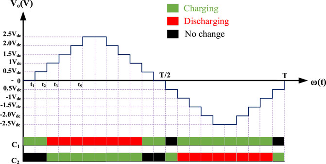
FIGURE 3. Staircase output with capacitor voltage pattern.
The charging and discharging of the
Where the LDP
Using LDP for C1, we can say that the maximum rate of discharge for capacitor
where the load current is represented by
Using Eq. 3, the values of capacitors C1 and C2 can be calculated as
The solution of Eq. 4 gives the optimal value of the capacitors by assuming the maximum permitted ripple voltage
4 Nearest level control pulse width modulation (NLCPWM)
Various control schemes have been tried and employed for multilevel inverters. The Nearest Level Control Pulse Width Modulation (NLCPWM) is a low-switching-frequency PWM approach, whose incorporation is simpler for higher levels (Hussan et al., 2020). Here, the suggested topology uses NLCPWM to govern the switching signals and generate the necessary output waveform. In NLCPWM, a sampled waveform is formed by comparing the standard sinusoidal waveform with the desired output waveform. To create switching pulses for the related IGBTs, the resulting waveform is then rounded off to the nearest level and analyzed using the switching logic shown in Table 1. Figures 4A, B depict the NLCPWM’s operating system. For this 11-level topology, the standard signal, which is a sine wave, has an amplitude of 5 and is assumed to have a frequency of 50 Hz.
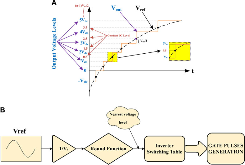
FIGURE 4. (A) Level generation method and (B) control scheme of NLCPWM.
5 Power loss analysis
For the proposed SCMLI topology, three different forms of losses—conduction loss, switching loss, charging or ripple loss—are taken into account.
5.1 Conduction or ohmic loss (
The internal resistances of the devices infiltrate the conduction route and create an ohmic loss.
where in Eq. 5,
5.2 Switching loss
Switching losses arise as a result of the switches’ switching activity. Taking into account the voltage and current of a linear switch at the time of switching, the switching power loss during the turn-on operation can be written using Eq. 6.
Power loss during the switching off procedure may be stated using Eq. 7.
where
5.3 Ripple or charging loss (
The loss occurring from the capacitor’s charge is known as the ripple loss or charging loss. The voltage difference between the capacitor’s current voltage and its intended voltage determines the magnitude of the charging current that flows through the capacitor during this time. The capacitors’ ripple loss during a fundamental cycle may be written as
where
Where time
6 Comparative analysis
To illustrate the aforementioned 11-level inverter benefits over existing topologies, a comparison with already reported 11-level topologies is made in this section. Table 2 presents a thorough assessment based on the number of switches (NSW), diodes (ND), DC sources (NDC), levels (NL), capacitors (NCP), the voltage gain of the converter, efficiency and total standing voltage (TSV) in p.u. The summation of all peak voltage stresses throughout all switches is known as total standing voltage (TSV). The voltage ratings of the switches to be incorporated in the topology is determined by this. TSV (p.u.) is the proportion of TSV to the AC output voltage peak value. The topologies are described in details in Table 2 in terms of comparative parameters. The topologies presented in Bana et al. (2020) require fewer switches compared to the proposed topology to produce an 11-level output voltage, but they also require an additional DC source and driver circuit. Also, it has less boosting capability and efficiency than the proposed topology. Although the work published in Alishah et al. (2016a) produces a greater number of levels than the proposed topology (Alishah et al., 2016a), requires a greater number of additional components, such as more DC sources, switches, driver circuits, diodes, and capacitors, which increases the overall cost of the inverter and makes it less efficient in terms of cost and reliability. The proposed topology and the topologies presented in Roy et al. (2019), Zamiri et al. (2016), Alishah et al. (2016b), and Siddique et al. (2020) both used the same number of switches and DC sources, but (Roy et al., 2019; Zamiri et al. 2016) were only able to generate 9 levels, which is less than the proposed topology, while the topology presented in Alishah et al. (2016b) is able to generate an 11-level output voltage waveform, which is the same as the proposed topology, but (Alishah et al., 2016b) lags in total device count, TSV(p.u.) and in efficiency as well. Similarly, the work presented in Siddique et al. (2020) produces 13 levels, which is more than the proposed topology, but it lags in both the number of driver circuits and efficiency. The proposed topology validates its superiority in comparison in terms of the lower requirement for the number of driver circuits to make the gating pulses for the switches than all other topologies. The proposed SCMLI topology has a gain of 1.67, which is higher than other published topologies except the topologies presented in Lee et al. (2019), which makes it more applicable to use in those areas where the requirement for output voltage is greater than input voltage. Likewise, in terms of efficiency, the proposed topology performs well except for the one presented in Sandeep and Yaragatti (2018), making it more suitable for use in real-world applications than other topologies. Also, except (Bana et al., 2020), (Siddique et al., 2020), (Zamiri et al., 2016) and (Sandeep and Yaragatti, 2018) the proposed topology outperforms in terms of TSV (p.u.) comparison. Additionally, considering the resistive load (R-load), the comparison of power rating for different topologies has also been mentioned in Table 2. Hence, the superiority of the proposed topology can be validated from this. For a purely resistive load, the power factor is equal to 1.
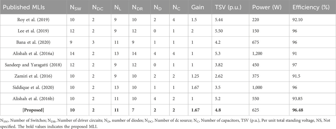
TABLE 2. Comparison of proposed inverter with recent topologies.
Overall, the choice of an MLI design depends on the specific application requirements, such as power rating, output voltage quality, circuit complexity, and cost-effectiveness. The studies presented in the table provide a useful reference for selecting the appropriate MLI design based on these considerations.
7 Results and discussion
This section presents the hardware and simulation results of the proposed 11-level inverter topology for various loading scenarios.
7.1 Simulation results
The voltage stress across the different switches used in the proposed topology has been shown in Figure 5. The suggested topology is simulated for 11-level using MATLAB/Simulink software. Figure 6 displays a variety of simulation results achieved for the 11-level SCMLI topology. Figure 6A depicts the output voltage and current waveforms of the proposed 11-level inverter for a purely resistive load (R = 50 Ω). As it is clear from Figure 6A, the output voltage waveform of the SCMLI has 11 levels, each level corresponding to a different voltage magnitude. The voltage waveform is a stepped waveform that approximates a sine wave and results in low harmonic distortion, which makes it suitable for applications that require high-quality voltage waveform. The current waveform also approximates a sinusoidal waveform with the same frequency as the output voltage waveform. Since the load is resistive, the current is proportional to the voltage, and the phase angle between the voltage and current waveforms is zero. The current waveform also has very low harmonic distortion, as the voltage waveform has low harmonic distortion and the load is purely resistive.
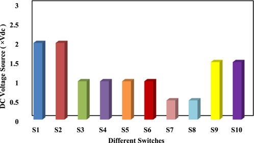
FIGURE 5. Voltage stress across the switches.
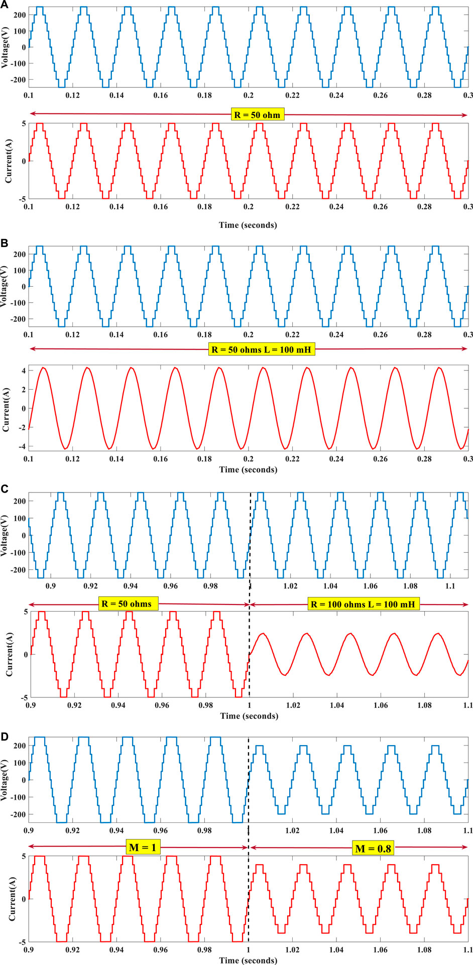
FIGURE 6. Waveforms of the output voltage and current of the proposed 11-level inverter for the following loads: (A) a 50-Ω resistive load; (B) an RL load (R = 50 Ω, L = 100 mH); (C) a dynamic load change from R = 50 Ω to R = 100 Ω and L = 100 mH; and (D) a modulation change from M = 1.0 to M = 0.8.
Figure 6B depicts the voltage and current waveform for an RL load with values of R = 50 ohm and L = 100 mH. Due to the inductance of the load, the voltage waveform is shifted in phase with respect to the current waveform. The degree of phase shift depends on the inductance value and the frequency of the voltage waveform. The current waveform approximates a sine wave more than the voltage waveform with the same frequency as the output voltage waveform and results in low harmonic distortion.
Figure 6C depicts the voltage and current waveform with dynamic load change from load resistance, R = 50 Ω to R = 100 Ω and load inductance L = 100 mH. When the R-load is changed to an RL load, the dynamics of the circuit change. In an R-load, the load current is proportional to the voltage, and the power factor is 1. However, in an RL load, the load current lags the voltage due to the presence of inductance, resulting in a lower power factor. This change in the load impedance affects the operation of the SCMLI, which may require adjustments in its control strategy to maintain efficient and stable operation. Specifically, the switching frequency and duty cycle of the inverter may need to be adjusted to maintain a desired output voltage level and minimize harmonic distortion.
Figure 6D depicts how changing the modulation values from M = 1.0 to M = 0.8, affects the system. When the modulation index is changed from 0.8 to 1.0, the output levels remain same, but the amplitude of current and voltage waveforms are changed proportionally. This means that the output power is changed as well. However, the waveform shape and phase angle between the voltage and current waveforms will remain unchanged. Table 3 displays many simulation-related characteristics.
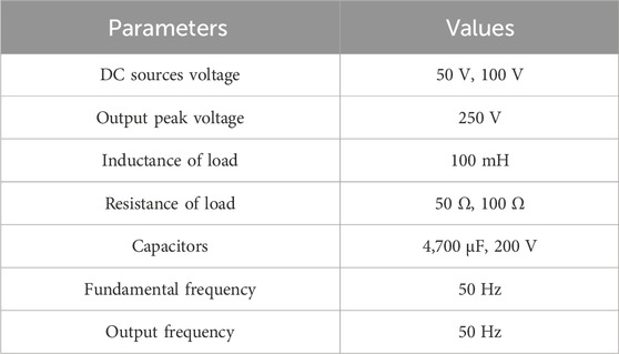
TABLE 3. Simulation parameters.
7.2 Hardware results
Figure 7 illustrates the hardware prototype that has been developed to evaluate the practicality of the proposed 11-level SCMLI. The circuit was developed using an insulated-gate bipolar transistor (IGBT) (FGA25N120). A gate driver circuit based on the TLP-250H was utilized to provide the gate signals for the individual IGBTs. Gate signals were created using the NLCPWM approach for fundamental switching. A digital signal processor (TMS320F28379D) was used to execute the NLC scheme for the suggested inverter. A FLUKE 435 Series II power quality and energy analyzer was used to test the experimental THD and efficiency percentages of the proposed MLI. The parameters for experimental setup are included in Table 4. For an input voltage of 40 V, the voltage gains of 1.67 is verified by the output voltage and output current waveform for the proposed 11-level topology, which is shown in Figure 8A. Figure 8B illustrates the transition in the load’s nature, going from an R-load to an RL-load, or from a power factor of unity to a lagging power factor of 0.95. Figure 8B shows that when the load switches from an R to an RL, there is no change in the voltage, but the current does smooth out due to inductive nature of load. The suggested inverter has been examined for several modulation indices, some of which are shown in Figure 8C. The number of output levels is observed to decrease from 11 to 9 when the modulation index is altered from 1 to 0.8. For a modulation index of 0.92–1, eleven levels are achieved at the output; this number drops to nine for a modulation index range from 0.72 to 9. The output voltage and current THD are shown in Figures 8D, E. When a RL load of 50 Ω and 100 mH was taken, it was discovered that the output voltage THD is 7.65% and the output current THD is 0.89%. By employing a power quality and energy analyzer the plot of efficiency at various loads against output power is achieved in Figure 8F. The greatest efficiency is 96.48% at 500 W of output power, and it becomes inferior as output power gets bigger due to the reason mentioned in (Reddy et al., 2020). The self-balancing of the capacitor voltage is proven by all of these waveforms. Additionally, the suggested design performs well under various loading scenarios. Table 4 lists the parameters for experimental analysis and validation for the proposed inverter.
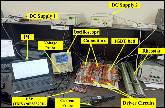
FIGURE 7. Experimental test bench of the proposed inverter.
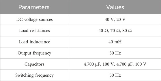
TABLE 4. Experimental validation Parameters.
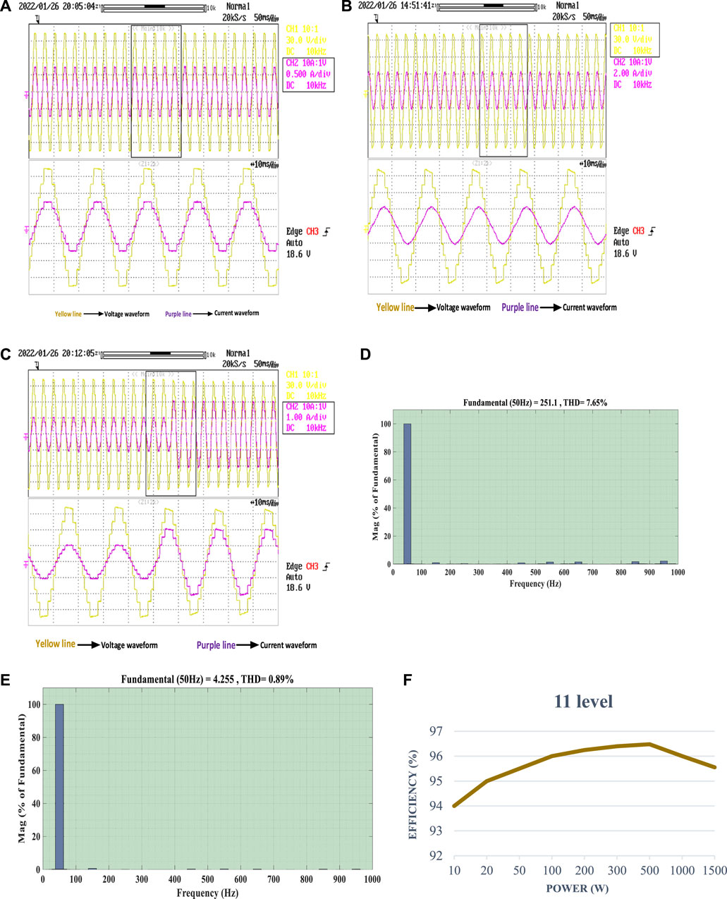
FIGURE 8. The output voltage and current waveforms of the proposed 11-level inverter for the following conditions: (A) a resistive load of 50 Ω; (B) an RL-load of R = 100 Ω and L = 100 mH; (C) a change in modulation from M = 1.0 to M = 0.8 (D) The output voltage’s THD (E) The output current’s THD and (F) efficiency under various loading scenarios.
8 Application of proposed SCMLI
This section outlines the inverter current control method for injecting active and reactive power from sources of distributed power generation into the grid. The inverter is linked to the grid and has eleven levels. V1 and V2 are the input voltage supplies taken from solar cells of the proposed multilevel inverter and the voltages are maintained at Vdc and Vdc/2. Figure 9 depicts the block diagram of the present control approach used to regulate the grid power injection.
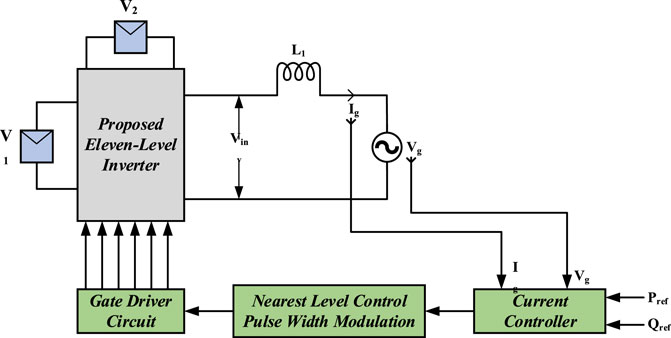
FIGURE 9. The grid-connected operation of the proposed eleven-level SCMLI.
The Phase-Locked Loop (PLL) block, which divides the grid voltage (Vg) into two components that are 90° apart, provides the grid voltage. The current controllers provide the NLCPWM block with a reference sine wave by delivering reference active (Pref) and reactive (Qref) power in accordance with the varying active power and reactive power demand values (Monfared et al., 2012; Kar et al., 2022). Both active and reactive power are controlled using the proportional-resonant (PR) controller, which has a lower computational cost.
Figure 10 depicts the block diagram for the NLCPWM reference sine wave generation process. In order to supply the necessary gate switching pulses for the inverter switches, the current-controlled reference signal is fed back as the reference signal of the NLC-PWM method. The appropriate gate driver circuit of the inverter receives the switching pulse produced by the NLCPWM block.
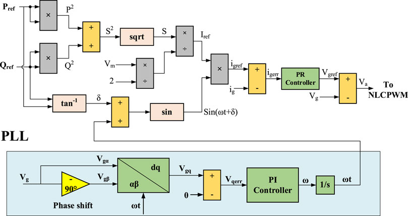
FIGURE 10. The technique for producing a reference sine wave for NLCPWM.
9 Conclusion
The work proposes an 11-level switched capacitor multilevel inverter (SCMLI) topology for solar PV application. The proposed topology employing a dual DC-source configuration with 8 unidirectional and 2 bidirectional switches to accomplish 1.67 times boosted operation. A comparison study is carried out to ascertain the effectiveness of the suggested MLI with the recent converters. All the capacitors used in circuit are self-balanced, which lessens the control complexity. A simple basic modulation approach i.e., NLCPWM is used to generate the gating pulses for IGBTs. The validation of the suggested 11-level MLI is accomplished under diverse operating circumstances with the aid of an experimental prototype. The suggested inverter output voltage and current are having THD of 7.65% and 0.89%, respectively. The optimum efficiency attained by the SCMLI is 96.48% at 500 W of output power. In the future, SCMLIs may become more widely adopted in renewable energy systems such as solar and wind power, as well as electric vehicles and energy storage systems. Research efforts may focus on improving the design and control of SCMLIs to enhance their performance, reduce their size and cost, and increase their reliability. Furthermore, the development of new materials and components could enable the creation of more advanced SCMLI topologies with even greater efficiency and power density.
Data availability statement
The original contributions presented in the study are included in the article/Supplementary Material, further inquiries can be directed to the corresponding authors.
Author contributions
MH: Conceptualization, Formal Analysis, Investigation, Methodology, Validation, Visualization, Writing–original draft. MT: Conceptualization, Formal Analysis, Investigation, Methodology, Supervision, Validation, Visualization, Writing–review and editing. AS: Conceptualization, Formal Analysis, Investigation, Methodology, Supervision, Validation, Visualization, Writing–review and editing. SA: Formal Analysis, Funding acquisition, Project administration, Validation, Visualization, Writing–review and editing. MP: Formal Analysis, Investigation, Validation, Visualization, Writing–review and editing. HM: Formal Analysis, Funding acquisition, Project administration, Visualization, Writing–review and editing.
Funding
The author(s) declare financial support was received for the research, authorship, and/or publication of this article. This research has received funding from King Saud University through Researchers Supporting Project number RSP2024R387), King Saud University, Riyadh, Saudi Arabia.
Acknowledgments
The authors extend their appreciation to King Saud University for funding this work through Researchers Supporting Project number (RSP2024R387), King Saud University, Riyadh, Saudi Arabia.
Conflict of interest
The authors declare that the research was conducted in the absence of any commercial or financial relationships that could be construed as a potential conflict of interest.
Publisher’s note
All claims expressed in this article are solely those of the authors and do not necessarily represent those of their affiliated organizations, or those of the publisher, the editors and the reviewers. Any product that may be evaluated in this article, or claim that may be made by its manufacturer, is not guaranteed or endorsed by the publisher.
References
Ali, M., Tariq, M., Lodi, K. A., Chakrabortty, R. K., Ryan, M. J., Alamri, B., et al. (2021). Robust ANN-based control of modified PUC-5 inverter for solar PV applications. IEEE Trans. Ind. Appl. 57, 3863–3876. doi:10.1109/TIA.2021.3076032
Alishah, R. S., Hosseini, S. H., Babaei, E., and Sabahi, M. (2016b). A new general multilevel converter topology based on cascaded connection of submultilevel units with reduced switching components, DC sources, and blocked voltage by switches. IEEE Trans. Ind. Electron. 63, 7157–7164. doi:10.1109/TIE.2016.2592460
Alishah, R. S., Hosseini, S. H., Babaei, E., Sabahi, M., and Zare, A. (2016a). Extended high step-up structure for multilevel converter. IET Power Electron 9, 1894–1902. doi:10.1049/iet-pel.2015.0893
Bana, P. R., Panda, K. P., and Panda, G. (2020). Power quality performance evaluation of multilevel inverter with reduced switching devices and minimum standing voltage. IEEE Trans. Ind. Inf. 16, 5009–5022. doi:10.1109/TII.2019.2953071
Chappa, A., Gupta, S., Sahu, L. K., Gautam, S. P., and Gupta, K. K. (2021). Symmetrical and asymmetrical reduced device multilevel inverter topology. IEEE J. Emerg. Sel. Top. Power Electron. 9, 885–896. doi:10.1109/JESTPE.2019.2955279
Gupta, K. K., Ranjan, A., Bhatnagar, P., Sahu, L. K., and Jain, S. (2016). Multilevel inverter topologies with reduced device count: a review. IEEE Trans. Power Electron. 31, 135–151. doi:10.1109/TPEL.2015.2405012
Hosseinzadeh, M. A., Sarebanzadeh, M., Rivera, M., Babaei, E., and Wheeler, P. (2021). A reduced single-phase switched-diode cascaded multilevel inverter. IEEE J. Emerg. Sel. Top. Power Electron. 9, 3556–3569. doi:10.1109/JESTPE.2020.3010793
Hussan, M. R., Sarwar, A., Khan, I., Tariq, M., Tayyab, M., and Alhosaini, W. (2021b). An eleven-level switched-capacitor inverter with boosting capability. Electron 10, 2262. doi:10.3390/electronics10182262
Hussan, M. R., Sarwar, A., Siddique, M. D., Iqbal, A., and Alamri, B. (2021a). A cross connected asymmetrical switched-capacitor multilevel inverter. IEEE Access 9, 96416–96429. doi:10.1109/ACCESS.2021.3093826
Hussan, M. R., Sarwar, A., Siddique, M. D., Mekhilef, S., Ahmad, S., Sharaf, M., et al. (2020). A novel switched-capacitor multilevel inverter topology for energy storage and smart grid applications. Electron 9, 1703–1718. doi:10.3390/electronics9101703
Iqbal, A., Siddique, M. D., Prathap Reddy, B., Maroti, P. K., and Alammari, R. (2020). A new family of step-up hybrid switched-capacitor integrated multilevel inverter topologies with dual input voltage sources. IEEE Access 9, 4398–4410. doi:10.1109/ACCESS.2020.3046192
Jagabar Sathik, M., Sandeep, N., Almakhles, D., and Blaabjerg, F. (2020). Cross connected compact switched-capacitor multilevel inverter (C3-SCMLI) topology with reduced switch count. IEEE Trans. Circuits Syst. II Express Briefs 67, 3287–3291. doi:10.1109/TCSII.2020.2988155
Jayabalan, M., Jeevarathinam, B., and Sandirasegarane, T. (2017). Reduced switch count pulse Width modulated multilevel inverter. IET Power Electron 10, 10–17. doi:10.1049/iet-pel.2015.0720
Kar, P. K., Priyadarshi, A., and Karanki, S. B. (2022). Control strategy for single-phase grid-interfaced modified multilevel inverter topology for distributed power generation. IEEE Syst. J. 16, 1627–1636. doi:10.1109/JSYST.2021.3091486
Khenar, M., Taghvaie, A., Adabi, J., and Rezanejad, M. (2018). Multi-level inverter with combined T-type and cross-connected modules. IET Power Electron 11, 1407–1415. doi:10.1049/iet-pel.2017.0378
Lee, S. S., Lee, K. B., Alsofyani, I. M., Bak, Y., and Wong, J. F. (2019). Improved switched-capacitor integrated multilevel inverter with a DC source string. IEEE Trans. Ind. Appl. 55, 7368–7376. doi:10.1109/TIA.2019.2893850
Mohamed Ali, J. S., and Krishnasamy, V. (2019). Compact switched capacitor multilevel inverter (CSCMLI) with self-voltage balancing and boosting ability. IEEE Trans. Power Electron. 34, 4009–4013. doi:10.1109/TPEL.2018.2871378
Monfared, M., Sanatkar, M., and Golestan, S. (2012). Direct active and reactive power control of single-phase grid-tie converters. IET Power Electron 5, 1544–1550. doi:10.1049/iet-pel.2012.0131
Ounejjar, Y., Al-Haddad, K., and Grégoire, L. A. (2011). Packed U cells multilevel converter topology: theoretical study and experimental validation. IEEE Trans. Ind. Electron. 58, 1294–1306. doi:10.1109/TIE.2010.2050412
Panda, N., Das, B., Chakrabarti, A., Kasari, P. R., Bhattacharya, A., and Chatterjee, D. (2021). A new grid interactive 11-level hybrid inverter topology for medium-voltage application. IEEE Trans. Ind. Appl. 57, 869–881. doi:10.1109/TIA.2020.3040204
Priyadarshi, A., Kar, P. K., and Karanki, S. B. (2020). A single source transformer-less boost multilevel inverter topology with self-voltage balancing. IEEE Trans. Ind. Appl. 56, 1–3965. doi:10.1109/TIA.2020.2988012
Reddy, B. P., Siddique, M. D., Iqbal, A., Mekhilef, S., Rahman, S., and Maroti, P. K. (2020). 7L-SCBI topology with minimal semiconductor device count. IET Power Electron 13, 3065–3071. doi:10.1049/iet-pel.2020.0313
Roy, T., Sadhu, P. K., and Dasgupta, A. (2019). Cross-switched multilevel inverter using novel switched capacitor converters. IEEE Trans. Ind. Electron. 66, 8521–8532. doi:10.1109/TIE.2018.2889632
Samadaei, E., Kaviani, M., and Bertilsson, K. (2019). A 13-levels module (K-type) with two DC sources for multilevel inverters. IEEE Trans. Ind. Electron. 66, 5186–5196. doi:10.1109/TIE.2018.2868325
Sandeep, N., and Yaragatti, U. R. (2018). A switched-capacitor-based multilevel inverter topology with reduced components. IEEE Trans. Power Electron 33, 5538–5542. doi:10.1109/TPEL.2017.2779822
Sharifzadeh, M., and Al-Haddad, K. (2019). Packed E-cell (PEC) converter topology operation and experimental validation. IEEE Access 7, 93049–93061. doi:10.1109/ACCESS.2019.2924009
Siddique, M. D., Mekhilef, S., Sarwar, A., Alam, A., and Shah, N. M. (2020). Dual asymmetrical dc voltage source based switched capacitor boost multilevel inverter topology. IET Power Electron 13, 1481–1486. doi:10.1049/iet-pel.2019.1567
Siddique, M. D., Mekhilef, S., Shah, N. M., and Memon, M. A. (2019). Optimal design of a new cascaded multilevel inverter topology with reduced switch count. IEEE Access 7, 24498–24510. doi:10.1109/ACCESS.2019.2890872
Tayyab, M., Sarwar, A., Murshid, S., and Al-Durra, A. “A novel single-source eleven-level quintuple-boost inverter with reduced component count,” in 2022 IEEE IAS Global Conference on Emerging Technologies (GlobConET), Arad, Romania, May, 2022, 605–609. doi:10.1109/GlobConET53749.2022.9872393
Tayyab, M., Sarwar, A., Murshid, S., Tariq, M., Al-Durra, A., and Bakhsh, F. I. (2023). Active and reactive power control of grid-connected single-phase asymmetrical eleven-level inverter. IET Gener. Transm. Distrib. 17, 632–644. doi:10.1049/gtd2.12442
Vahedi, H., Labbé, P. A., and Al-Haddad, K. (2016). Sensor-less five-level packed U-cell (PUC5) inverter operating in stand-alone and grid-connected modes. IEEE Trans. Ind. Inf. 12, 361–370. doi:10.1109/TII.2015.2491260
Vemuganti, H. P., Sreenivasarao, D., Ganjikunta, S. K., Suryawanshi, H. M., and Abu-Rub, H. (2021). A survey on reduced switch count multilevel inverters. IEEE Open J. Ind. Electron. Soc. 2, 80–111. doi:10.1109/OJIES.2021.3050214
Ye, Y., Chen, S., Wang, X., and Cheng, K. W. E. (2021). Self-balanced 13-level inverter based on switched capacitor and hybrid PWM algorithm. IEEE Trans. Ind. Electron. 68, 4827–4837. doi:10.1109/TIE.2020.2989716
Keywords: multilevel inverter, switched-capacitor topology, total standing voltage, voltage boosting, inverter, solar photo-voltaic
Citation: Hussain MT, Tariq M, Sarwar A, Ahmad S, Poshtan M and Mahmoud HA (2024) A dual source fed eleven level switched capacitor multilevel inverter with voltage boosting capability. Front. Energy Res. 11:1326554. doi: 10.3389/fenrg.2023.1326554
Received: 23 October 2023; Accepted: 31 December 2023;
Published: 11 January 2024.
Edited by:
Fazal Akbar, University of Edinburgh, United KingdomReviewed by:
Faramarz Faraji, Kyungpook National University, Republic of KoreaFazal Akbar, University of Edinburgh, United Kingdom
Copyright © 2024 Hussain, Tariq, Sarwar, Ahmad, Poshtan and Mahmoud. This is an open-access article distributed under the terms of the Creative Commons Attribution License (CC BY). The use, distribution or reproduction in other forums is permitted, provided the original author(s) and the copyright owner(s) are credited and that the original publication in this journal is cited, in accordance with accepted academic practice. No use, distribution or reproduction is permitted which does not comply with these terms.
*Correspondence: Mohd Tariq, dGFyaXEuZWVAemhjZXQuYWMuaW4=; Adil Sarwar, YWRpbC5zYXJ3YXJAemhjZXQuYWMuaW4=