 Asif Ali
 Jianhui Su1*
 Amjad Ali
- 1School of Electrical Engineering and Automation, Hefei University of Technology, Hefei, China
- 2Department of Electrical Engineering, Mehran University of Engineering and Technology, Khairpur, Pakistan
- 3Department of Electrical Engineering, Southwest Jiaotong University, Chengdu, China
- 4Department of Electrical Engineering, Mehran University of Engineering and Technology, Jamshoro, Pakistan
High Frequency-Link (HFL) Inverters have been employed to integrate renewable energy sources into utility grids and electric vehicles. The soft-switching range of High-Frequency Link Inverters (HFLI) is increased using auxiliary inductors and capacitors. The application of auxiliary components increases the conduction loss and the complexity of the circuit. The literature indicates that the existing soft-switching methods suffer from higher duty cycle loss, voltage spikes, and lower efficiency owing to the resonance between the parasitic capacitance of switches and the leakage inductance of the transformer. Therefore, it is imperative to develop a modulation strategy that can improve the efficiency of HFLI. In this context, the proposed study develops a cycloconverter-type High-Frequency Link Inverter (CHFLI) based on a Bipolar Phase Shift Modulation (BPSM) strategy without the use of auxiliary components. The proposed modulation strategy enables the semiconductor switches to operate under zero voltage switching. The full-bridge inverter and Full Bridge Active Clamper Circuit (FBAC) switches operate at the same gating signals with a constant duty cycle of 50%. The proposed topology uses built-in magnetizing inductance to achieve zero voltage switching and reduce the duty cycle loss. The leakage energy is recycled from the output filter inductor to the load side using the FBAC. The results indicate that the proposed modulation strategy achieves ZVS and simultaneously achieves an efficiency of 95%. The proposed modulation strategy is easy to implement and does not require complex circuitry.
1 Introduction
Growing concerns over environmental issues and diminishing fossil fuels have stimulated the progress of Renewable Energy Resources (RES), such as photovoltaics, wind, and fuel cells. This development has attracted the attention of utilities worldwide, leading to a greater integration of RES into the utility grid. However, this integration necessitates the use of grid-tied inverters (Faranda et al., 2015; Pinto et al., 2016; Iyer et al., 2017; Meng et al., 2017). The most recent developments in inverters lack performance, efficiency, and power density (Qinglin et al., 2005). Inverters with line-frequency isolation transformers as depicted in Figure 1, are common in conventional utility grids. Therefore, this approach increases the inverters’ size, volume, and cost, which in turn jeopardizes the power density and efficiency.
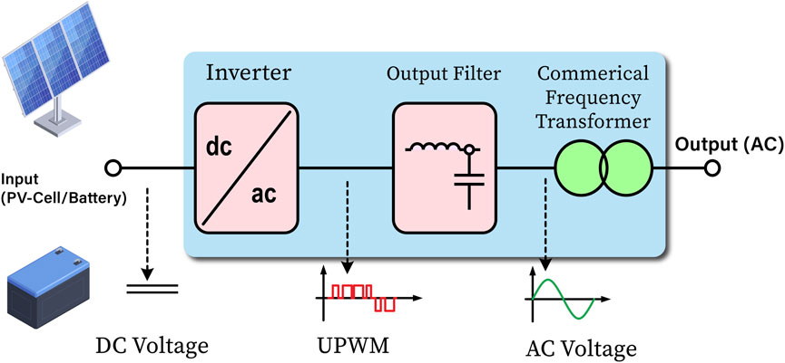
FIGURE 1. Conventional inverter with Commercial Line Frequency Transformer.
Inverters that employ HFL are designed to incorporate High-Frequency Transformers (HFT) for isolation. This arrangement offers advantages, such as reduced weight, smaller volume, higher power density, miniaturization, lower cost, excellent reliability, and improved efficiency, as highlighted in (Guo et al., 2018; Nayak et al., 2019; Wu et al., 2023). In addition to RES, HFL inverters have been extensively utilized in compact power conversion-based modules for applications in naval, space, and energy storage systems (Mazumder and Rathore, 2011). HFLI inverters are categorized into three groups based on their power conversion stages and circuit structures. The first structure is the conventional HFL inverter, which comprises three steps that insert an HFT between the DC/AC and AC/DC stages as given in Table 1, the configuration I. Conventional HFL inverters typically have three power conversion stages, resulting in reduced efficiency and increased inverter size owing to a bulky intermediate LC filter with high cost (Kan et al., 2014; Zhu et al., 2014; Zhou et al., 2018). The conventional inverter design has been modified to reduce both the size and cost; this modification involves the removal of the intermediate LC filter, which is typically bulky and costly. The alternative is given in Table 1, with configuration II, and is referred to as a rectifier-type high-frequency link (RHFL) inverter (Guo et al., 2018; Chen et al., 2016a).
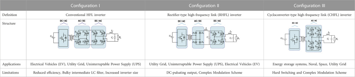
TABLE 1. Types of high-frequency link inverters.
Eliminating the LC filter reduces the inverter size; however, as a result, the DC-pulsating output poses a challenge in devising a modulation approach for the inverter (Zhou et al., 2018). Multiple clamping circuits have been suggested in the existing literature to enhance the effectiveness of pulsating DC voltage removal on the secondary side, as referenced in (Huang and Mazumder, 2008; Wang et al., 1999). The Cycloconverter-type high-frequency link inverter (CHFLI) topology is composed of a primary-side inverter and a secondary-side cycloconverter with a high-frequency transformer (HFT) interposed between them, is given in Table 1, with configuration III, and is known for its high efficiency, compact size, and lightweight characteristics (Kan et al., 2014; Zhu et al., 2014; Zhou et al., 2018; Yamato et al., 1990).
The CHFL is commonly utilized in standalone photovoltaic systems that require a high level of efficiency to offset the low efficiency of photovoltaic panels (Rocabert et al., 2004). In a previous work (Aganza-Torres and Cárdenas, 2011) a high-frequency link inverter with a multiple carrier modulation scheme for low-power (RES) applications was presented. However, during the commutation period of cycloconverter switches, zero crossing distortion was observed in output voltage. Two types of modulation techniques are utilized in CHFL inverters to enhance the efficiency of switching operations and enable natural commutation for bidirectional switches in cycloconverters (Guo et al., 2018; Zhu et al., 2014; Tao et al., 2021). The primary modulation techniques used by inverters to generate gating signals are Unipolar Pulse Width Modulation (UPWM) and bipolar pulse-width modulation (BPWM) (Zhu et al., 2014; Kan et al., 2014; Mazumder et al., 2010; Yan et al., 2012; Basu and Mohan, 2014).
The three-level output generated by the Unipolar Pulse Width Modulation (UPWM) technique is a frequently applied modulation strategy for a Cascaded H-Bridge Full-bridge (CHFL) inverter. This approach enables bidirectional cyclo-converter switches to achieve natural commutation during the zero level of the modulation signal, thereby facilitating efficient Zero Voltage Switching (ZVS) (Guo et al., 2018; Guo et al., 2016). A Unipolar Pulse Width Modulation (UPWM)-based soft-switching push-pull high-frequency link inverter was proposed in (Chen et al., 2016a). Owing to the rectification of the modulating signal, the output voltage quality was inappropriate (Chen et al., 2016a). A PSM-type UPWM-based inverter was proposed in (Guo et al., 2016), which does not require rectification of the modulating signals, but two auxiliary inductors were used to extend ZVS range at light load conditions. Addition of auxiliary inductor increases the component count for inverter. The inverter proposed in (Guo et al., 2016) has low power level, and cannot be used in renewable energy applications.
The commutation of the load current in the cycloconverter continues to yield voltage spikes on bidirectional switches (Guo et al., 2018; Wang et al., 2018). Overlap commutation switching techniques have been implemented in previous studies (Mazumder and Rathore, 2011; Zhu et al., 2014; Guo et al., 2016) to achieve zero voltage switching (ZVS) of bidirectional switches in cycloconverters. However, a resonance issue arises between the leakage inductance of the transformer and the output capacitance of the bidirectional switches, leading to electromagnetic interference (EMI) (Gandikota and Mohan, 2014; Korkh et al., 2019; Wang et al., 2022).
In (Yamato et al., 1990), switches on both the primary and secondary sides were subjected to hard-switching conditions, resulting in elevated switching losses during high-frequency applications. The authors in (Zhou et al., 2018; Wang et al., 1999) proposed a primary-side phase-shift full-bridge inverter and a secondary-side active clamp circuit (ACC) to achieve soft switching. In (Zhu et al., 2022), primary full bridge inverter switches were operated under hard switching conditions, and the duty cycle of the (ACC) switches is not fixed at 50%, but instead varies from 0 to 1. However, it is challenging for primary-side switches to achieve soft switching under light-load conditions (ul Hassan et al., 2021). In (Guo et al., 2018), a proposal is presented for a high-frequency link inverter of the cycloconverter-type that utilizes wide-range soft-switching high-efficiency (UPWM) technology. The asymmetric phase-shift modulation strategy (APSM) was proposed in (Xiao et al., 2023) to extend the ZVS range; however, it increases the complexity of the modulation circuit. The paper in (Azizipour and Hojabri, 2023) presents a Push Pull type high-frequency link inverter with primary and secondary side switches that undergo hard switching. The resulting output voltage contains a significant amount of harmonics. The proposal of high-frequency link inverter utilizing space vector modulation (SVM) is given in (Jin et al., 2023) aimed to alleviate the current stress on cycloconverter switches, despite the operation of semiconductor switches under hard switching conditions. A de-recoupling based model predictive control scheme for high-frequency link inverters was introduced in (Fu et al., 2022), but it requires complex analytical calculations to determine the optimal vector for generating switching signals.
In (Guo et al., 2018; Sabate et al., 1991), the authors used an auxiliary inductor on the primary side of the full-bridge inverter to achieve the zero voltage switching (ZVS) range of the primary switches. The auxiliary circuit amplifies the complexity and expense of the system (Zhong et al., 2018). Unipolar Pulse Width Modulation (UPWM) creates the problem of zero-crossing distortion and a narrow pulse on the transformer’s primary side (Guo et al., 2018; Zhu et al., 2014; Guo et al., 2016). Leakage inductance is another factor contributing to duty cycle loss, resulting in a decreased effective duty cycle on the secondary side. The duty cycle on the primary side of the inverter is indicated by D, where ΔD represents the loss of the duty cycle, as shown in Eq. 1, (Zhao et al., 2015). Furthermore, the effective duty cycle is expressed as
The voltage ratio of the transformer input to output depends on the effective duty cycle, as determined by Eq. (3), (Guo et al., 2016).
A comprehensive review of the literature shows that various HFLI topology-based topologies have been employed in the existing literature. However, they suffer from the following limitations.
• Existing studies (Guo et al., 2018; Zhu et al., 2014; Guo et al., 2016) have adopted the Unipolar Pulse Width Modulation (UPWM)-based soft-switching strategy, which suffers from higher duty-cycle losses. During the switched-on state, a voltage drop occurs across the switches, and energy is lost in the form of heat.
• The available literature (Nayak et al., 2019; Wang et al., 2018) indicates that ZVS can be achieved at higher loads; however, to achieve ZVS at lighter loads, the leakage inductance is increased by adding an additional inductor or capacitor. The addition of auxiliary components increases the complexity of the circuit.
• The existing literature (Nayak et al., 2019; Korkh et al., 2019) indicates that losing zero voltage switching (ZVS) significantly increases switching and conduction losses. Voltage spikes are also generated owing to the resonance between the parasitic capacitance and transformer leakage inductance.
Therefore, the proposed study utilizes a Bipolar Phase Shift Modulation (BPSM) strategy with the development of a soft-switched cycloconverter-type high-frequency link inverter (HFLI). The contributions of this study are as follows.
• Development of an efficient cycloconverter-based BPSM to achieve ZVS with minimal duty cycle loss.
• Development of a full-bridge active clamper circuit for minimizing the voltage stress on the cyclo-converter switches and simultaneously recycling the leakage energy of the inductor output filter.
• Design of simplified and practically feasible Bipolar Phase Shift modulation (BPSM) strategy that enables the operation of all switches at a constant duty cycle of 50%.
• The performance of the proposed BPSM modulation strategy is benchmarked against some recent and widely used state-of-the-art modulation strategies.
The bipolar (PSM) modulation has a lower total harmonic distortion (THD) and exhibits better output voltage quality when compared to other modulation techniques. The modulation scheme utilizes only one reference signal and one carrier signal, which facilitates easy implementation. Additionally, the proposed modulation strategy does not exhibit pulse drops around the zero crossing of the output voltage, thereby minimizing duty cycle loss. As a result of these advantages, bipolar PSM has a higher efficiency and lower distortion in the output voltage.
The remainder of this paper is organized as follows. Section 2 discusses the proposed topology and respective modulation technique. Section 3 presents the operation modes of the proposed topology and modulation strategy. Section 4 examines the soft-switching, steady-state conditions of the switches and efficiency of the proposed topology. Finally, Section 5 presents the conclusions of the study.
2 Methodology
2.1 Proposed modulation strategy
The circuit diagram of the proposed high-frequency link inverter topology is shown in Figure 2. The

FIGURE 2. Proposed soft switched CHFL inverter.
The proposed full bridge inverter configuration comprises of four MOSFET switches, represented as
The full wave cyclo-converter type configuration is formed by the switches
A resistive load, denoted by
2.2 Proposed modulation strategy
The proposed new bipolar phase shift modulation strategy is presented in Figure 3, where
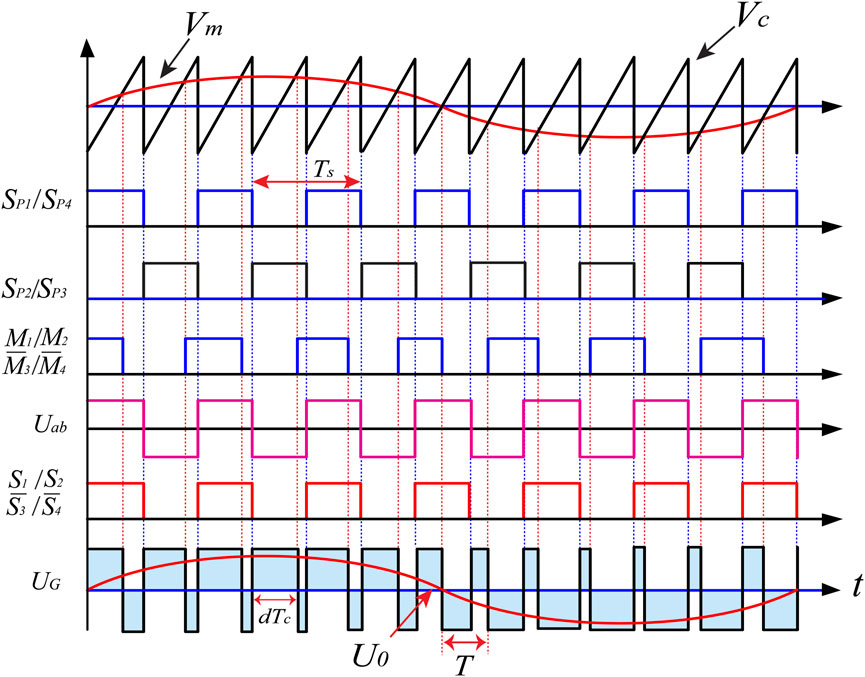
FIGURE 3. Modulation waveforms of Proposed BPSM.
The primary full bridge inverter switches are driven by comparing the carrier and modulating signals, with the primary switches being operated at a 50% duty cycle ratio. The gating signals for switches
2.3 Switching signal generation strategy
The proposed gating signal generation strategy for creating gating signals for semiconductor switches is illustrated in Figure 4. This process involves the use of two comparators to generate a clock signal for two flip-flops. The upper Comparator-I receives the carrier and modulating signals at its input.
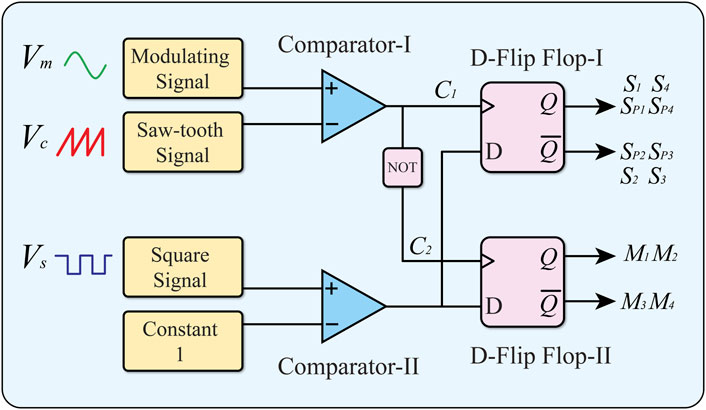
FIGURE 4. Gating signal diagram for proposed BPSM.
3 Operational principle of the proposed inverter
The operational principle of the proposed inverter is presented by assuming that all MOSFET switches are ideal and that their output capacitances are uniform.
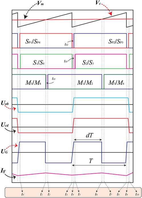
FIGURE 5. Operation modes of proposed inverter.
FIGURE 6. Equivalent Circuits of Operational Modes in one switching cycle (A) Interval 1
Interval 1 [
The expression for the current
The voltage
Interval 2 [
Where
This results in the discharge of the output capacitance (switch
Interval 3 [
Interval 4 [
Interval 5 [
4 Results and discussion
A Simulink model is designed in MATLAB 2021b to demonstrate the effectiveness of the proposed topology; the values and parameters of the various components utilized in the model are listed in Table 2.

TABLE 2. Circuit parameters for simulation.
4.1 ZVS of full bridge inverter switches
The amount of power lost during hard switching of the MOSFET switches is given by Eq. (15).
ZVS of Full bridge inverter switches depends mainly on magnetizing inductance current
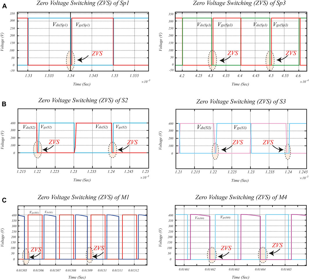
FIGURE 7. Zero Voltage switching (A) (ZVS) waveforms of Full Bridge Inverter
The equivalent energy must be present to discharge the switches’ output capacitance, as given in Eq. (18)
4.2 ZVS of full bridge active Clamper Switches
The zero voltage switching (ZVS) waveform of the Full Bridge Active Clamper (FBAC) switches
Consequently, a substantial increase in the ZVS range can be achieved by increasing the value of the leakage inductance. Switch
4.3 ZVS of cyclo-converter switches
The voltage across the parasitic capacitance of the cycloconverter switch is observed to be zero, which leads to the switches achieving the zero voltage switching (ZVS) state during the deadtime period
The boundary conditions ensuring ZVS condition of cycloconverter switches
ZVS boundary of cycloconverter switches,
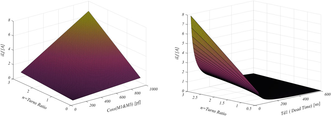
FIGURE 8. ZVS boundary of Cycloconverter Switches
4.4 Steady-state waveforms
The driving signals for switches
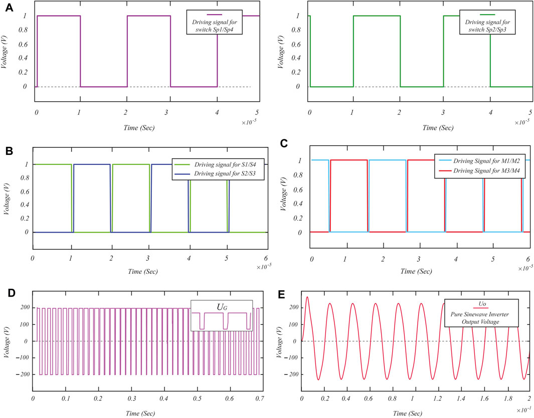
FIGURE 9. Key Waveforms (A) Gating Signals of Primary Side Inverter Switches (
The following Eq. 22 can mathematically represent the
Unipolar Pulse Width Modulation (UPWM) creates a narrow pulse at the zero crossing of the output voltage (Zhu et al., 2014). It is observed that if the rise-ON time of the semiconductor switch is higher than that of a narrow pulse, then this narrow pulse is lost. In the case of the BSPM, there was no loss of a narrow pulse. As shown in Figure 10A,
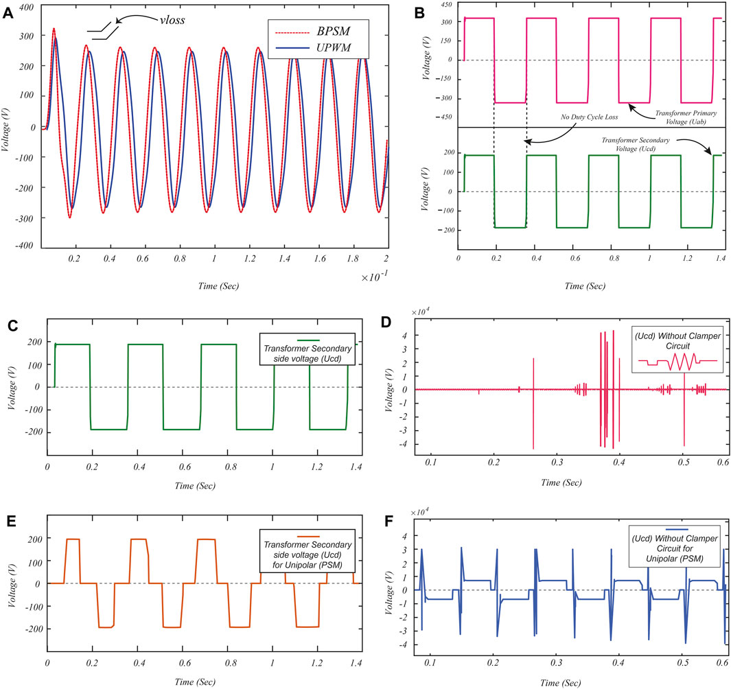
FIGURE 10. (A) Comparison of output voltage
The comparison of steady state waveforms for a conventional high frequency link inverter and the proposed inverter is also presented in Figure 10. In Figure 10C, the transformer secondary voltage of the proposed inverter based on Bipolar (PSM) with a clamper circuit is depicted, which shows there is no any voltage spike on transformer secondary side voltage. Conventional high frequency link inverter when operated at high switching frequency without clamper circuit, high value voltage spikes are created, many times larger than nominal voltage, as shown in Figure 10D. The steady state waveforms for the conventional high frequency link inverter when operated under Unipolar modulation are presented in Figures 10E, F.
The transient behaviour of the proposed inverter is analysed from full-load to no-load and no-load to full-load conditions verified using the simulation results. Output voltage
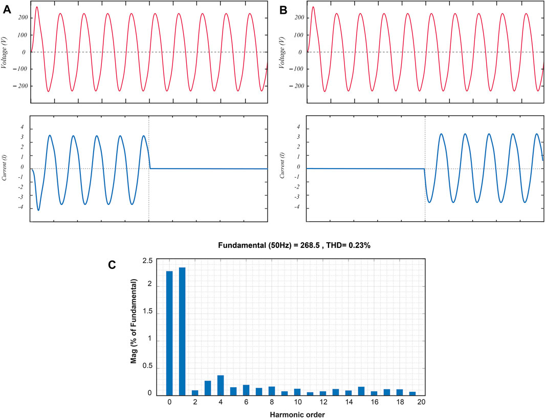
FIGURE 11. Transient waveforms of output voltage
4.5 Benchmarking against recent UPWM strategies
For the practical implementation of a High-Frequency Link Inverter (HFLI), it is imperative to consider the problems related to the realization of a wide ZVS range, voltage spikes on cycloconverter switches, duty-cycle loss, and high leakage inductance. Various solutions have been reported in the literature (Guo et al., 2018; Zhu et al., 2014); however, all require additional components (i.e., Diodes, Auxiliary inductors, and capacitors). Additional components make the topology more complex; therefore, practical realization is difficult. Moreover, sufficient leakage inductance energy is required to discharge the parasitic capacitance of semiconductor switches. Under light loads, an auxiliary inductor is required to achieve a Wide ZVS range. The proposed strategy uses magnetizing inductance to realize a wide ZVS range, without the addition of any auxiliary inductor.
Different Active clamp circuits (ACC) have been reported in the literature (Wang et al., 1999; Mazumder et al., 2010) to suppress voltage spikes. However, the control schemes for operating ACC are complex, and the ZVS of ACC switches is difficult to realize. The proposed Full Bridge Active Clamper circuit (FBAC) has 50% duty cycle control signals. It is possible to realize a wide range of ZVS without relying on the load current, and reduced conduction and duty cycle loss lead to higher efficiency and higher power density.
The features of our proposed (BPSM) based (CHFLI) with other recently developed topologies and modulation strategies are presented in Table 3.
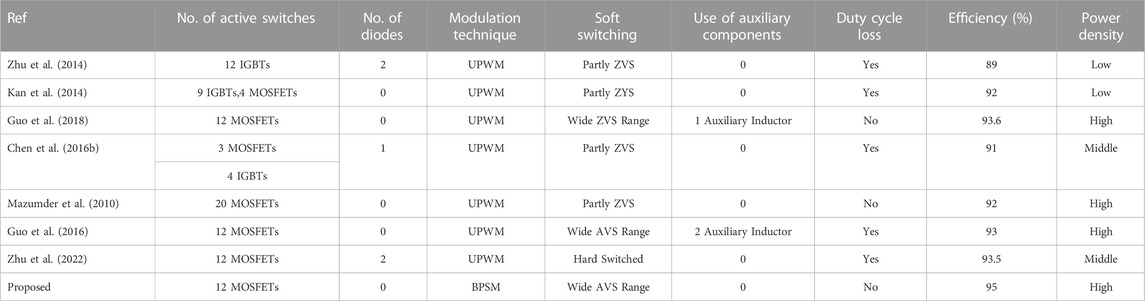
TABLE 3. Benchmarking of proposed inverter against dc-ac UPWM based inverter.
The efficiency of the proposed inverter is shown in Figure 12. It can be observed that the highest efficiency of the proposed inverter is higher than that of the inverter in (Zhu et al., 2014), which simultaneously improves the power density. The proposed inverter is controlled using a simple modulation strategy that achieves zero voltage switching (ZVS) over a wide load range.
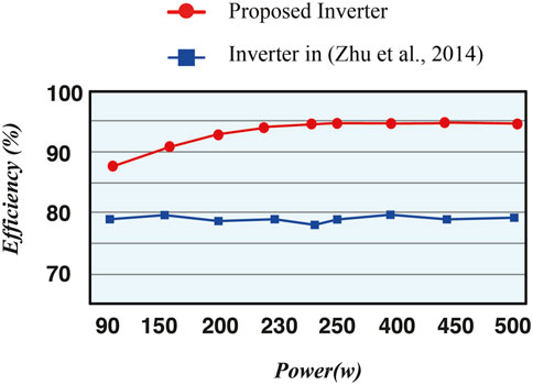
FIGURE 12. Efficiency of proposed inverter.
5 Conclusion
HFLI inverters are used for the integration of renewable sources with smart grid networks. Recently developed HFLI designs have auxiliary components; therefore, these strategies suffer from complex designs and high duty cycle losses. The proposed design focuses on a High-frequency link inverter featuring a novel bipolar phase shift modulation strategy (BPMS). To facilitate the operation of primary full-bridge inverter switches at 50% duty cycle while ensuring zero voltage switching (ZVS). The proposed design was comprehensively investigated through operational modes, modulation strategies, and soft-switching analysis of power semiconductor switches employed in circuit configurations. It is observed that the proposed topology experience lower duty cycle loss. The Full Bridge Active Clamper (FBAC) circuit was designed precisely to solve the problem of voltage spikes and stress on the secondary side of cycloconverter switches. One of the key advantages of FBAC is its ability to recycle energy from the output filter inductor back to either the DC or the AC side. The simulation results verified that the ZVS of semiconductor switches has been achieved without any auxiliary component. The proposed scheme achieves an efficiency of 95% and minimum duty cycle losses. In the future, the proposed modulation strategy can be extended to achieve a higher efficiency with advanced and sophisticated power electronic switches.
Data availability statement
The raw data supporting the conclusion of this article will be made available by the authors, without undue reservation.
Author contributions
Conceptualization AsA and JS. Writing, reviewing, and editing AsA GY, PH, visualization AsA, AmA. All authors contributed to the article and approved the submitted version.
Conflict of interest
The authors declare that the research was conducted in the absence of any commercial or financial relationships that could be construed as a potential conflict of interest.
Publisher’s note
All claims expressed in this article are solely those of the authors and do not necessarily represent those of their affiliated organizations, or those of the publisher, the editors and the reviewers. Any product that may be evaluated in this article, or claim that may be made by its manufacturer, is not guaranteed or endorsed by the publisher.
References
Aganza-Torres, A., and Cárdenas, V. (2011). “Analysis and modelling of HF-link cycloconverter based inverter for low-power renewable energy sources applications,” in Proceedings of the CCE 2011 - 2011 8th International Conference on Electrical Engineering, Computing Science and Automatic Control, Merida City, Mexico, October, 2011. doi:10.1109/ICEEE.2011.6106602
Azizipour, O., and Hojabri, H. (2023). Single phase high frequency AC link DC/AC converter for photovoltaic systems. Electr. Power Components Syst. 51 (1), 59–70. doi:10.1080/15325008.2022.2160522
Basu, K., and Mohan, N. (2014). A high-frequency link single-stage PWM inverter with common-mode voltage suppression and source-based commutation of leakage energy. IEEE Trans. Power Electron 29 (8), 3907–3918. doi:10.1109/TPEL.2013.2280600
Chen, Z., Wu, Q., and Yuan, Y. (2016a). A novel zero-voltage-switching push–pull high-frequency-link single-phase inverter. IEEE J. Emerg. Sel. Top. Power Electron 4 (2), 421–434. doi:10.1109/JESTPE.2015.2505171
Chen, Z., Wu, Q., and Yuan, Y. (2016b). A novel zero-voltage-switching push-pull high-frequency-link single-phase inverter. IEEE J. Emerg. Sel. Top. Power Electron 4 (2), 421–434. doi:10.1109/JESTPE.2015.2505171
Faranda, R. S., Hafezi, H., Leva, S., Mussetta, M., and Ogliari, E. (2015). The optimum PV plant for a given solar DC/AC converter. Energies (Basel) 8 (6), 4853–4870. doi:10.3390/en8064853
Fu, T., Yan, Z., Pashajavid, E., and Ali, L. (2022). “De-Re-Coupling scheme-based model predictive control of a three-phase high-frequency link matrix converter,” in Proceedings of the 2022 IEEE Sustainable Power and Energy Conference, iSPEC 2022, Perth, Australia, December, 2022. doi:10.1109/iSPEC54162.2022.10032976
Gandikota, S., and Mohan, N. (2014). “A new leakage energy commutation technique for single stage high frequency link inverters,” in Proceedings of the 2014 IEEE International Conference on Power Electronics, Drives and Energy Systems, PEDES 2014, Mumbai, India, December 2014. doi:10.1109/PEDES.2014.7042126
Guo, S., Su, J., Chen, X., and Yu, X. (2016). Soft-switching Single-Stage three-level power amplifier for High-Voltage audio distribution systems. Electron Lett. 52 (21), 1797–1799. doi:10.1049/el.2016.2220
Guo, S., Su, J., Lai, J., and Yu, X. (2018). Analysis and design of a wide-range soft-switching high-efficiency high-frequency-link inverter with dual-phase-shift modulation. IEEE Trans. Power Electron 33 (9), 7805–7820. doi:10.1109/TPEL.2017.2771765
Huang, R., and Mazumder, S. K. (2008). “A novel soft-switching scheme for an isolated DC/DC converter with pulsating DC output for a three-phase high-frequency-link PWM converter,” in Proceedings of the IEEE Industry Applications Society Annual Meeting, Edmonton, AB, Canada, October, 2008, 1–9. doi:10.1109/08IAS.2008.303
Iyer, K. v., Baranwal, R., and Mohan, N. (2017). A high-frequency AC-link single-stage asymmetrical multilevel converter for grid integration of renewable energy systems. IEEE Trans. Power Electron 32 (7), 5087–5108. doi:10.1109/TPEL.2016.2609881
Jin, P., Hu, Y., Lei, G., Guo, Y., and Zhu, J. (2023). A novel SVM strategy to reduce current stress of high-frequency link matrix converter. IEEE Trans. Industrial Electron., 1–10. doi:10.1109/TIE.2023.3279581
Kan, J., Xie, S., Wu, Y., Tang, Y., Yao, Z., and Chen, R. (2014). High-frequency-link inverter using combined synchronous rectifiers. IEEE Trans. Industrial Electron. 61 (12), 6769–6777. doi:10.1109/TIE.2014.2320233
Korkh, O., Blinov, A., and Vinnikov, D. (2019). “Analysis of oscillation suppression methods in the AC-AC stage of high frequency link converters,” in Proceedings of the IEEE 60th International Scientific Conference on Power and Electrical Engineering of Riga Technical University (RTUCON), Riga, Latvia, October 2019, 1–5. doi:10.1109/RTUCON48111.2019.8982259
Mazumder, S. K., Burra, R. K., Huang, R., Tahir, M., and Acharya, K. (2010). A universal grid-connected fuel-cell inverter for residential application. IEEE Trans. Industrial Electron. 57 (10), 3431–3447. doi:10.1109/TIE.2009.2038943
Mazumder, S. K., and Rathore, A. K. (2011). Primary-side-converter-assisted soft-switching scheme for an AC/AC converter in a cycloconverter-type high-frequency-link inverter. IEEE Trans. Industrial Electron. 58 (9), 4161–4166. doi:10.1109/TIE.2010.2098375
Meng, Z., Wang, Y., Yang, L., and Li, W. (2017). Analysis of power loss and improved simulation method of a high frequency dual-buck full-bridge inverter. Energies (Basel) 10, 311–313. doi:10.3390/en10030311
Nayak, P., Rajashekara, K., and Pramanick, S. K. (2019). Soft-switched modulation technique for a single-stage matrix-type isolated DC-AC converter. IEEE Trans. Industry Appl. 55, 7642–7656. doi:10.1109/TIA.2018.2889977
Pinto, R., Mariano, S., Calado, M. D. R., and de Souza, J. F. (2016). Impact of rural grid-connected photovoltaic generation systems on power quality. Energies (Basel) 9 (9), 739. doi:10.3390/en9090739
Qinglin, Z., Yunhua, X., Xiaoyi, J., and Weiyang, W. (2005). “DSP-based closed-loop control of Bi-directional voltage mode high frequency link inverter with active clamp,” in Proceedings of the Conference Record - IAS Annual Meeting (IEEE Industry Applications Society), Hong Kong, China, October, 2005, 928–933. doi:10.1109/IAS.2005.1518456
Rocabert, J., Dumenjó, M. M., Bordonau, J., and Beristáin, J. A. (2004). “A regenerative active clamp circuit for DC/AC converters with high-frequency isolation in photovoltaic systems,” in Proceedings of the PESC Record - IEEE Annual Power Electronics Specialists Conference, Aachen, Germany, June 2004, 2802–2808. doi:10.1109/PESC.2004.1355439
Sabate, J. A., Vlatkovic, V., Ridley, R. B., and Lee, F. C. (1991). “High-voltage, high-power, ZVS, full-bridge PWM converter employing an active snubber,” in Proceedings of the APEC ’91: Sixth Annual Applied Power Electronics Conference and Exhibition, Dallas, TX, USA, March, 1991, 158–163. doi:10.1109/APEC.1991.146157
Tao, P., Cui, Y., and Liang, J. (2021). Research on efficient soft switching based on MPPT of PV power generation system. Front. Energy Res. 9. doi:10.3389/fenrg.2021.728789
ul Hassan, T., Cheema, K. M., Mehmood, K., Tahir, M. F., Milyani, A. H., and Akhtar, M. (2021). Optimal control of high-power density hybrid electric vehicle charger. Energy Rep. 7, 194–207. doi:10.1016/j.egyr.2020.12.021
Wang, K., Lee, F. C., and Dong, W. (1999). “A new soft-switched quasi-single-stage (QSS) bi-directional inverter/charger,” in Proceedings of the Conference Record of the 1999 IEEE Industry Applications Conference Thirty-Forth IAS Annual Meeting (Cat No.99CH36370), Phoenix, AZ, USA, October 1999, 2031–2038. doi:10.1109/IAS.1999.806016
Wang, M., Huang, Q., Guo, S., Yu, X., Yu, W., and Huang, A. Q. (2018). Soft-switched modulation techniques for an isolated bidirectional DC-AC. IEEE Trans. Power Electron 33 (1), 137–150. doi:10.1109/TPEL.2017.2661965
Wang, Y., Liu, H., and Wheeler, P. (2022). Research on the voltage spike suppression strategy for three-phase high frequency link matrix-type inverter. IEEE J. Emerg. Sel. Top. Power Electron 10 (5), 6070–6083. doi:10.1109/JESTPE.2022.3155249
Wu, F., Wang, K., Hu, G., Shen, Y., and Luo, S. (2023). Overview of single-stage high-frequency isolated AC-DC converters and modulation strategies. IEEE Trans. Power Electron 38 (2), 1583–1598. doi:10.1109/TPEL.2022.3210745
Xiao, Y., Guan, Y., and Qin, L. (2023). Proposed asymmetric phase shift modulation strategy to improve zero-voltage-switch range and transmission power range for dual active bridge converter. Energy Rep. 9, 762–770. doi:10.1016/j.egyr.2023.04.194
Yamato, I., Tokunaga, N., Matsuda, Y., Suzuki, Y., and Amaro, H. (1990). “High frequency link DC-AC converter for UPS with a new voltage clamper,” in Proceedings of the 21st Annual IEEE Conference on Power Electronics Specialists, San Antonio, TX, USA, August, 1990, 749–756. doi:10.1109/PESC.1990.131264
Yan, Z., Jia, M., Zhang, C., and Wu, W. (2012). An integration SPWM strategy for high-frequency link matrix converter with adaptive commutation in one step based on De-Re-coupling idea. IEEE Trans. Industrial Electron. 59 (1), 116–128. doi:10.1109/TIE.2011.2158775
Zhao, L., Li, H., Liu, Y., and Li, Z. (2015). High efficiency variable-frequency full-bridge converter with a load adaptive control method based on the loss model. Energies (Basel) 8 (4), 2647–2673. doi:10.3390/en8042647
Zhong, S., Xu, J., and Zhou, X. (2018). High-efficiency zero-voltage switching single-stage switching amplifier with half-bridge active clamping circuit. IEEE Trans. Industrial Electron. 65 (11), 8574–8584. doi:10.1109/TIE.2018.2815953
Zhou, X., Xu, J., and Zhong, S. (2018). Single-Stage soft-switching low-distortion bipolar PWM modulation high-frequency-link DC-AC converter with clamping circuits. IEEE Trans. Industrial Electron. 65 (10), 7719–7729. doi:10.1109/TIE.2018.2801807
Zhu, W., Cao, X., Li, X., Li, Y., Xu, Y., and Zhou, K. (2022). Analysis and suppression of voltage harmonic distortions of the single-phase high frequency link matrix-type DC-AC converter. IEEE Access 10, 130273–130284. doi:10.1109/ACCESS.2022.3229489
Keywords: soft switching, high-frequency-link (HFL) inverter, bipolar (PSM), full bridge active clamper circuit (FBAC), zero voltage switching (ZVS)
Citation: Ali A, Su J, Yang G, Ali A and Hameed Shaikh P (2023) Soft switching modulation strategy based on bipolar (PSM) with improved efficiency in high-frequency link inverters. Front. Energy Res. 11:1252819. doi: 10.3389/fenrg.2023.1252819
Received: 04 July 2023; Accepted: 19 October 2023;
Published: 02 November 2023.
Edited by:
Maissa Farhat, American University of Ras Al Khaimah, United Arab EmiratesReviewed by:
Bin Duan, Shandong University, ChinaHussain Attia, American University of Ras Al Khaimah, United Arab Emirates
Copyright © 2023 Ali, Su, Yang, Ali and Hameed Shaikh. This is an open-access article distributed under the terms of the Creative Commons Attribution License (CC BY). The use, distribution or reproduction in other forums is permitted, provided the original author(s) and the copyright owner(s) are credited and that the original publication in this journal is cited, in accordance with accepted academic practice. No use, distribution or reproduction is permitted which does not comply with these terms.
*Correspondence: Jianhui Su, c3VfY2hlbkAxMjYuY29t