 Weiqi Wang
 Xiaoting Xia
 Shuling Rui2
 Xiangjian Meng
- 1College of Electrical Engineering and Automation, Shandong University of Science and Technology, Qingdao, China
- 2State Grid Shandong Electric Power Company, Qingdao, China
High-power current source inverters (CSI) usually operate at a low switching frequency to reduce switching loss. To suppress low-order harmonics and simplify filter design, the selective harmonic elimination pulse width modulation (SHEPWM) technique is a feasible common modulation strategy in industrial applications. This paper proposes an operational strategy that uses an H7 current source inverter (H7-CSI) with hybrid switches to perform the SHEPWM technique. On the basis of retaining the conventional H6 inverter bridge, the commutation speed of the CSI is improved by an additional shunt-connected high-performance power switch. The proposed scheme solves the problem that the CSIs built with low-speed switches (such as GTOs) may have difficulty for implementing the setting pulse widths of null states, while further reducing the switching losses at an acceptable cost. In addition, mitigating the influence of overlap-time by optimizing the driving signal of the H6 converter bridge. Finally, simulation and experiments have verified the effectiveness of the proposed CSI scheme.
1 Introduction
With the emergence of the worldwide energy shortage crisis, more and more attention has been paid to renewable energy (Shahbaz et al., 2020). Under the future trend of the energy revolution, power inverters are playing a vitally important role in the future grid (Sahan et al., 2011). From the form of power supply on the DC side, inverters can be classified as voltage source inverter (VSI) and current source inverter (CSI). Compared to VSI, CSI has the advantages of boosting voltage capability and high reliability (Zmood and Holmes, 2001; Azmi et al., 2011), and it is considered to have potential application value in renewable energy conversion, e.g., photovoltaic (Sahan et al., 2008; Lorenzani et al., 2017), wind energy, and ocean energy systems.
At present, the primary problem of CSI is the high power loss of switching devices, which mainly owing to the fact that CSI has to hold the circuit with a constant current (Trzynadlowski et al., 2001). There are two main technical routes to solve the efficiency problem: One is to replace all the switches with advanced semiconductor devices (e.g., Silicon Carbide (SiC) and Gallium Nitride (GaN) power switches but leaving great burden on the hardware cost of the equipment (Abu-Khaizaran and Palmer, 2007; Mudholkar et al., 2014; Hazra et al., 2016; Guacci et al., 2019). Another one is to try to make CSI work at a much lower switching frequency (Espinoza and Joos, 1997). However, it carries the risk of reducing power quality. With the introduced large amount of low-order harmonics, the filters are more difficult to design.
The selective harmonic elimination pulse width modulation (SHEPWM) technique is one of the effective solutions to address the above challenges. It is characterized by low switching frequency and excellent harmonic performance, particularly suitable for high-power applications that mitigate switching loss by reducing switching frequency (Pontt et al., 2004; Dahidah et al., 2015). During the implementation of SHEPWM, there are two key issues that need to be considered: one is the establishment of the switching sequence model which determines the harmonic performance, and another is the solution of non-linear transcendental equations which determines the difficulty and accuracy of realization. Karshenas, H. and Kojori, H. investigated the unique characteristics of CSI commutation, and carried out the general CSI switching sequence models (Karshenas et al., 1995). Over the past few decades, scholars have proposed many fruitful methods to find the optimal solutions. Siddique, M.D. using a particle swarm optimization (PSO) algorithm to calculate switching angles. (Siddique et al., 2021). The Newton-Raphson iterative algorithm is the most commonly used method to solve the equations, which needs to find the initial value to fast convergence. Maswood, A.I. proposed using Genetic Algorithm to find the initial switching angels (Maswood et al., 2001). In addition, optimized switching angles are calculated using APSO-GA for seven-level and nine-level inverter (Memon et al., 2022).
Operated with SHEPWM, CSI can effectively eliminate low-order harmonics in theory. However, due to the low switching speed of CSI power switches in practical application, the actual output performance is usually inconsistent with the expectation, some low-order harmonics still occupy a large proportion. This paper analyzes this phenomenon and proposes a new SHEPWM implementation scheme to improve the commutation speed through H7-CSI with hybrid semiconductor switches. Compared to the conventional low-speed switch-based CSIs, the proposed scheme can promote the commutation speed without excessive hardware cost to obtain a better output performance.
This rest of paper is organized as follows. In Section 2, it describes the general SHEPWM implementation process of conventional H6-CSI, and analyzes the limitation of switching speed on modulation. In Section 3, the operational principles of SHEPWM with H7-CSI as well as the hardware configurations are presented in detail. In Section 4, simulation and experimental tests are carried out to validate the theoretical findings.
2 SHEPWM of conventional current source inverters
2.1 Conventional current source inverters topology and its switching combinations
The conventional three-phase CSI is also named as H6-CSI, the topology is shown in Figure 1. It usually uses a voltage power supply and a DC-link inductor to achieve the approximately constant current source Idc. H6 inverter bridge can realize the current commutation and output the three-phase switched currents ia, ib, ic. After the AC filter capacitor Ca, Cb, Cc, the output currents are iao, ibo, ico. For high-power CSI, H6 inverter bridge is mainly composed of six low-speed power switches (e.g., GTOs, IGCTs) (Xu et al., 2023). When IGBTs are selected, it requires series connected power diodes to increase the reverse-blocking (RB) capability.
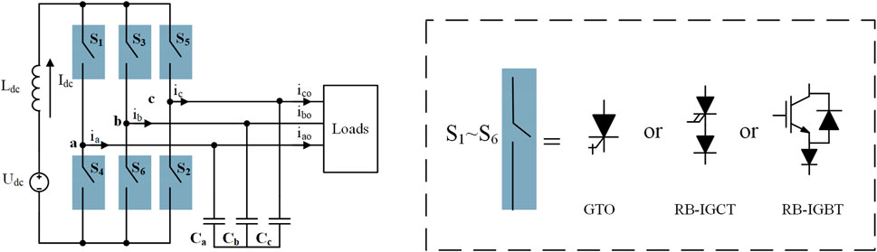
FIGURE 1. Conventional H6-CSI topology and hardware configurations.
At any moment during modulation, there are two switches conducting ON, one on the upper arms (S1 or S3 or S5), and another on the lower arms (S4 or S6 or S2). And CSI adopts lateral commutation mode among the bridge arms. There are nine switching states in total, six of which are active states ({S1, S2}, {S1, S6}, {S2, S3}, {S3, S4}, {S4, S5}, {S5, S6}), the rest three are null states ({S1, S4}, {S2, S5}, {S3, S6}). It is worth noting that the null states actually behave as short-circuit status of the circuit, which is also denoted as the short-circuit pulses in this paper.
2.2 SHEPWM implementation method and the limitations
The SHEPWM method can remove low-order harmonics from the inverter’s output by setting the appropriate angles of switching operation. The conventional CSI SHEPWM method is implemented by introducing short-circuit pulses and setting transitions, which is completely different from VSI SHEPWM. Literature (Karshenas et al., 1995) have investigated and listed these differences in the SHEPWM between VSI and CSI in detail.
The operational steps of SHEPWM of conventional CSI are as follows. Step 1: select the low-order harmonics to be eliminated, and set the number of switching angles. N is the number of switching angles and also represents that (N-1) harmonics can be eliminated (e.g., setting N = 5 means to eliminate the harmonics of 5th, 7th, 11th, 13th). It is worth noting that, to maintain the continuity of the current, the switching angles should be set within (0, π/6). Step 2: build the pulse sequences. The characteristic of this scheme is that the driving signals of switches (S1 ∼ S6) lags π/3 in turn and the output waveform of three-phase current ia, ib and ic lags 2π/3 in turn. Step 3: formulate the output current i(ωt) expression, which owns the features of half-wave symmetry and quarter-wave symmetry. Fourier decomposition is performed on the output current i(ωt). The decomposition formula is shown as Eq. 1, where Ia,n is the amplitude of nth order harmonic of the output phase current ia, and Ia,n can be calculated by Eq. 2.
Denote the amplitude of the fundamental current as Ia,1. Then, the modulation index m can be expressed by Eq. 3. Thus, the switching angles under different modulation index can be solved.
The following takes N = 7 and N = 9 as examples to explain the specific implementation method. When N = 7, the harmonic orders to be eliminated are 5th, 7th, 11th, 13th, 17th, 19th. Therefore, seven switch angles are set (α1, α2, α3, α4, α5, α6, α7). The specific pulse sequence in a quarter of one period is shown in Figure 2A. The driving sequence of each power switch has four short-circuit pulses in one period. Ia,n can be formulated as Eq.4. Using Eq. 3 and Eq. 4, and set Ia,n = 0 (n = 5, 7, 11, 13, 17, 19), the switching angles can be solved out.
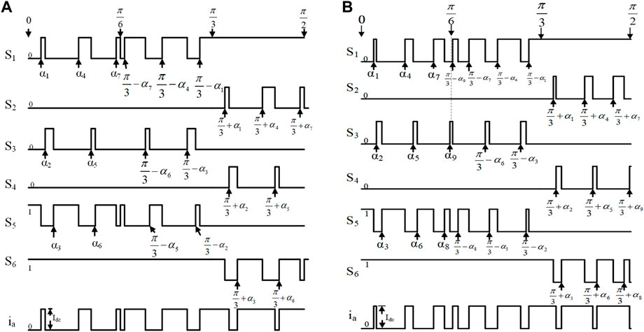
FIGURE 2. (A) SHEPWM scheme of H6-CSI (N = 7), (B) SHEPWM scheme of H6-CSI (N = 9).
Similarly, when N = 9, to eliminate harmonic of 5th, 7th, 11th, 13th, 17th, 19th, 23rd, 25th, the nth harmonic expression of the output current can be formulated as Eq.5. The specific pulse sequence in a quarter of one period is shown in Figure 2B. Compared to the previous sequence (N = 7), the driving pulses (N = 9) of switch S1 ∼ S6 become denser and have introduced more short-circuit pulses in one period.
The above is the modulation scheme under theoretical analysis and ideal conditions. In practical applications, the current of the switch can reflect the commutation process (Bernet et al., 1999). Since the power switch has turn-on time and turn-off time in actual operation, the current of the switch has a rising time (ton) and a falling time (toff), which are different from the ideal waveforms. The comparison between ideal and actual current waveforms are shown in Figure 3. The dwell time of an ideal driving pulse is recorded as ts, and the dwell time of the actual switching pulse is recorded as ta. Apparently, the effective pulse width of actual switching is shorter than the ideal setting dwell time. Therefore, the actual current rising and falling process can make the switching angles inconsistent with expectations.
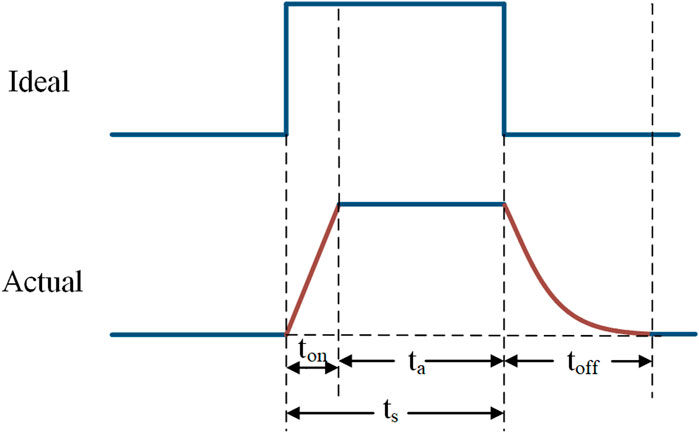
FIGURE 3. The comparison between ideal and actual current waveforms.
Since high-power CSIs are employed with low-speed switches, the turn-on and turn-off process can last up to a few microseconds. Furthermore, with the increase of the modulation index as well as the number of switching angles, the drive pulses become denser. In particular, the shortest pulse width comes from the null state, so that the completion of the short-circuit pulses will be significantly affected by the commutation speed of switches. For example, when m = 0.96 and N = 9, the shortest pulse width occurs at the short-circuit states, which has a width of only about 29 μs. Therefore, conventional CSI who built with low-speed switches (e.g., GTOs, IGCTs) may have difficulty in the switching speed to keep up with the setting short-circuit pulses width, so that the output current cannot reach the expected performance.
In addition, to maintain the continuity of the DC link current, the overlap-time has to be introduced between two switching signals during commutation (Suroso and Noguchi, 2020; Liu et al., 2021). To guarantee the commutation of the low-speed switches is completed, the delay of switching pulses caused by the overlap-time cannot be ignored as well. If not properly set, this phenomenon at short-circuit states will greatly worsen the total harmonic distortion (THD) performance. Therefore, the configuration of overlap-time also need to be carefully considered in conventional CSI.
3 Proposed SHEPWM operational principle with H7-CSI
3.1 Topology and hardware configurations
To improve the commutation speed of low-speed switches of SHEPWM-CSI, this paper proposes a new SHEPWM operational scheme based on the H7-CSI. The topology of the H7-CSI is shown in Figure 4. Compared to conventional CSI, the basic feature of the H7-CSI topology is the added shunt-connected seventh switch, which is the key to improve the inverter’s performance (Wang et al., 2018). The seventh switch is connected in parallel with the DC bus, which can be used to replace all the null states. Within 30° power factor angle range, when S7 is turned on, the current will be quickly switched to this branch, and the remaining six switches can turn on/off with zero current switching (ZCS) capability.
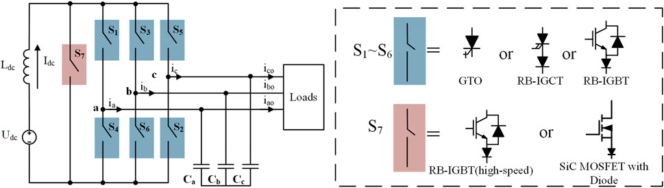
FIGURE 4. H7-CSI topology and hardware configurations.
In terms of hardware configuration, the six power switches in the H6 converter bridge retains the same (low-speed switches) configuration scheme as the conventional CSI. The key difference is that the seventh switch uses a high-performance power switch. This seventh switch should be characterized by high switching frequency and low loss, which can increase the inverter commutation speed while reducing switching loss. Available choices are high-speed RB-IGBT, or SiC MOSFET with Diode, etc. The reverse-blocking capability can be realized via series connected power diodes. Compared with the conventional all-hardware-update routine of CSI, the H7-CSI topological solution adopted in this paper can clearly reduce the hardware cost.
3.2 SHEPWM operational principle
The basic idea of proposed SHEPWM solution is to use the seventh switch to help the commutation of other low-speed switches. The specific operating principles are as follows.
1) Select the low-order harmonics to be eliminated, set the number of switching angles, then build the pulse execution scheme of switch S1∼S6 and formulate the expression of the output current i (ωt), which is basically the same as the conventional SHEPWM-H6-CSI method.
2) Pick out the short-circuit states among the calculated angles, and manage to use switch S7 to implement these null state pulses.
3) Optimize the driving signal of switch S1∼S6, regarding the overlap-time issue.
The overlap-time optimization process is pictured as Figure 5. Because the null-state pulses of S7 are inserted between two different active states (implemented by S1-S6), the adjacent turn-off and turn-on operation of S1-S6 can be extended with no impact to the output of the circuit. As shown in Figure 5, the original driving sequence is {Sx turn-off, S7 turn-on} to {S7 turn-off, Sy turn-on}. To optimize the driving signal, Sx should be delayed for shutdown, the delay time is denoted as td, while Sy should be turned on in advance, which is denoted as te. Both td and te should be set within (0, ts). And the pulse width of S7 itself remains unchanged. Doing so, on the one hand, it solves the overlap-time issue with no interference to the power quality, and on the other hand, the switching speed challenge of S1-S6 can get relieved.
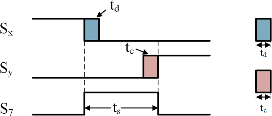
FIGURE 5. Overlap-time optimization scheme.
Normally, the delay time and advance time are set as 1–3 μs. Under the premise of meeting the requirements of the rules, the delay time and advance time can be optimized according to the switching speed of the switch.
According to the operating principles described above, pulse sequences of N = 7 and N = 9 can be rebuild, as shown in Figure 6A and Figure 6B. The optimized overlap-time is represented by the shaded area in Figure 6.
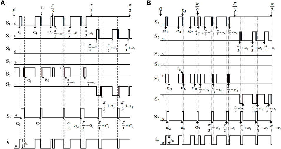
FIGURE 6. (A) SHEPWM sequences of H7-CSI (N = 7), (B) SHEPWM sequences of H7-CSI (N = 9).
The switching characteristics of the proposed SHEPWM scheme with H7-CSI and the conventional SHEPWM-H6-CSI are compared, as shown in Table 1. The proposed SHEPWM scheme basically uses S7 to improve the commutation speed around the null states, which would be affected by the switching speed most. Since S7 is characterized by fast switching speed and low switching loss, it is obvious that its actual performance is determined by the hardware selection of S7.

TABLE 1. Comparison of switching characteristics in one period.
As for the switching operation, compared to the conventional SHEPWM-H6-CSI, the total number of hard-switching counts of the proposed SHEPWM-H7-CSI is reduced by almost one-third. Moreover, most of the hard-switching transitions are implemented by S7, which can further reduce the switching loss. In addition, because the implementation of null states uses less power devices, the conduction loss can also decrease. Therefore, it indicates that the proposed SHEPWM-H7-CSI solution can even perform better efficiency.
4 Performance evaluation
4.1 Simulation results
To compare the performance between conventional SHEPWM-H6-CSI and the proposed SHEPWM operational method with H7-CSI, simulation models have been set up using MATLAB with PLECS Blockset, where H6-CSI and H7-CSI are built with the same parameters. The simulation parameters are listed in Table 2.
TABLE 2. Simulation parameters.
The conventional H6-CSI using the SHEPWM method is first simulated. The power circuitry is established by PLECS Blockset, which can simulate the turn-on and turn-off process of the power switches. To simulate the behavior of the self-controlled low-speed switches while taking the actual capabilities of the simulation environment into account, the power switch S1∼S6 are built with the “IGBT with Limited di/dt model”, where the “rise time” and “fall time” are configured with 10 s of microsecond. Other parasitic parameters (such as the blocking voltage, stray inductance, on-resistance, etc.) are modeled after the datasheet of typical low-speed switches. MATLAB is used to implement the driving-pulse sequences and analyze the output waveform.
Figure 7A shows the comparison of the output switched current ia (before the filters) at N = 7. The upper and lower waveforms represent the actual and ideal switched currents, respectively. A zoomed view of the two waveforms during (π/3, 2π/3) is demonstrated in Figure 7B. During this period, S1 remains on state, and S4 performs short-circuit pulses. As can been seen from the comparison, there exists a slight difference in the operating angles as well as the width of switching pulse. The same trend can also be found in Figure 8, which is the waveform comparison of the output switched current with N = 9. Therefore, the phenomenon of actual commutation difference caused by switching speed is reproduced.
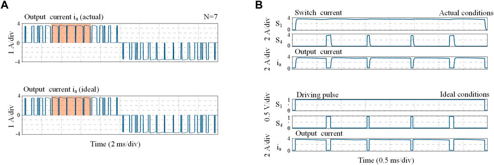
FIGURE 7. (A) Simulated output switched current ia of H6-CSI (N = 7), (B) Corresponding zoomed view within (π/3, 2π/3).
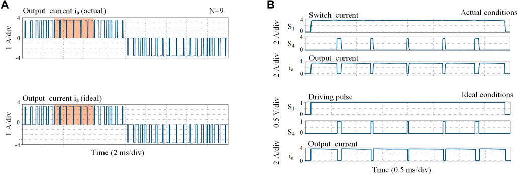
FIGURE 8. (A) Simulated output switched current ia of H6-CSI (N = 9), (B) Corresponding zoomed view within (π/3, 2π/3).
Figures 9A,B shows the actual filtered output three phase currents and voltages of H6-CSI using the SHEPWM methods at N = 7 and N = 9, respectively. Figures 9C,D are the corresponding FFT analysis results. These simulation results show that with the increase of switching angles, the pulse sequences become denser. If the low switching speed is taken into account, the low-order harmonics will not be eliminated entirely, which has the high contents of 5th and 7th harmonics.
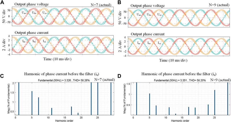
FIGURE 9. Simulated outputs (A) Filtered waveforms of conventional SHEPWM-H6-CSI with N = 7, (B) Filtered waveforms of conventional SHEPWM-H6-CSI with N = 9, (C) Harmonic performance of ia with N = 7, (D) Harmonic performance of ia with N = 9.
The following simulation are the verification of the proposed SHEPWM scheme based on H7-CSI method. The power circuitry of H7-CSI is also built in PLECS Blockset. Switch S7 is set with a shorter turn-on and turn-off time than that of S1∼S6. Taking N = 7 as an example, the output three-phase voltage and current after the capacitor filters are shown in Figure 10A. And the harmonics of the output current ia are analyzed by FFT which is shown in Figure 10B. When N = 9, the filtered output waveforms and harmonic analysis of H7-CSI are shown in Figures 10C,D, respectively. The contents of low-order harmonics to be eliminated have been compared and listed in Table 3, which can give a clear view of the harmonic differences. Observing from Figure 10, it can be found that the low-order harmonic contents are almost zero. Compared with the THD value of 58.26% for conventional SHEPWM-H6-CSI with low-speed switches in Figure 9C and Figure 10C, the THD value of proposed SHEPWM based on H7-CSI is 57.59% with the proposed modulation method. These THD values are 58.20% and 57.44% in Figure 9D and Figure 10D, respectively. It is worth noting that low-order harmonics content of 5th and 7th decreased significantly. To sum up, the low-order harmonics that to be eliminated are significantly reduced with the proposed solution. Therefore, the output power quality has been improved.
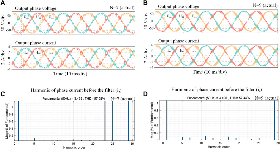
FIGURE 10. Simulated outputs (A) Filtered waveforms of proposed SHEPWM-H7-CSI with N = 7, (B) Filtered waveforms of proposed SHEPWM-H7-CSI with N = 9, (C) Harmonic performance of ia with N = 7, (D) Harmonic performance of ia with N = 9.
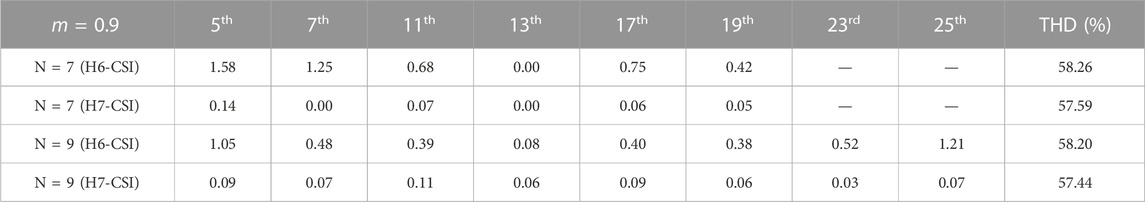
TABLE 3. Harmonic performance (% of fundamental).
4.2 Experimental verifications
To verify the performance of the proposed SHEPWM strategy with H7-CSI, an experimental prototype is established displayed in Figure 11. The parameter experimental settings are shown in Table 4. On the controller board, the gating sequences are programmed and implemented by an FPGA of xc3s500e from the family of XILINX Spartan3E. In the power circuitry, the DC inductor, the output capacitor filter and the output resistive loads are consistent with the simulation model. To perform the low switching speed of power switches, S1-S6 are selected with modular IGBTs (FF100R12RT4 from Infineon), and the driving resistance is set with 40 Ω S7 is employed by a silicon carbide power MOSFET (C2M0040120D from Cree).
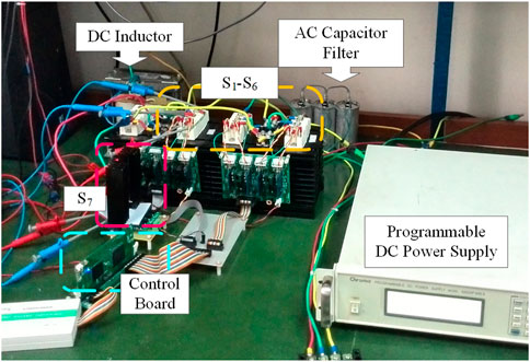
FIGURE 11. Experimental prototype of the H7-CSI.
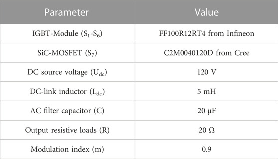
TABLE 4. Experimental parameters.
Figure 12 shows the experimental driving pulses of switches S7, S2, S6 respectively. In Figure 12, the modulation state sequence is from {S1, S2}, via {S7}, to {S1, S6}. As expected, S2 and S6 switch much slower than S7. To be specific, the turn-on and turn-off time of S2 and S6 are nearly 3 µs, while the switching speed of S7 is less than 200 ns.

FIGURE 12. Experimental waveforms of switching transition.
Set N = 7 for experimental verification, the gating pulses of switches S1, S5, S6 and S7 for one period are captured as Figure 13. It is easy to find that the experimental sequences are consistent with the theoretical settings, which have been presented in Figure 6. And the commutation features conform to the description in Table 1.
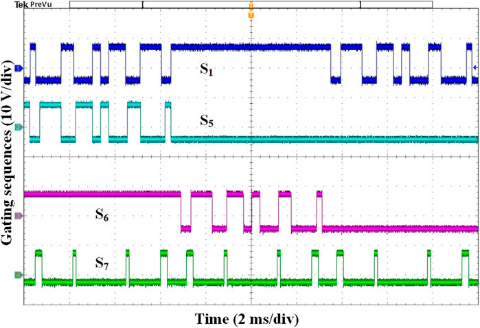
FIGURE 13. Experimental gating pulses sequences.
To go a step further, an additional experimental prototype of conventional H6-CSI with the same hardware has also been carried out to test and compare the harmonic performance. The experimental phase voltage, phase current and the current harmonic spectrum of conventional SHEPWM-H6-CSI with low-speed switches are shown in Figure 14A. The filtered voltage and current waveforms are basically complete sinusoidal waves. The burrs are due to the characteristics of low-speed switching operation. From the spectrum analysis, it can be clearly seen that the output current contains many harmonic components, and the harmonics of 5th, 7th, 11th, 13th still remains a certain content.
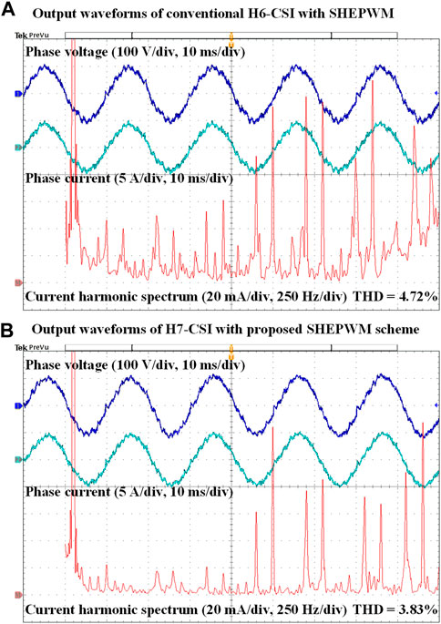
FIGURE 14. (A) Experimental output waveforms of conventional H6-CSI with SHEPWM, (B) Experimental output waveforms of conventional H7-CSI with SHEPWM.
By contrast, Figure 14B shows the experimental output waveforms of the proposed H7-CSI with SHEPWM. The inverter also outputs 50 Hz sinusoidal voltage and current. Although the waveforms are not significantly different from that of H6-CSI, spectral analysis shows that the proposed SHEPWM strategy has less harmonic contents. The THD value of output current has decreased from 4.72% to 3.83%. And the low order harmonics (5th, 7th, 11th, 13th) have almost been eliminated successfully. Thus, the harmonic performance of CSI can be improved with the proposed method.
5 Conclusion
This paper reviews the SHEPWM technique of conventional H6-CSI and investigates the practical effect of low switching speed on the harmonic elimination. In order to enhance the performance of SHEPWM, an operation strategy based on H7-CSI with hybrid switches has been proposed. It utilizes one high-speed switch and six conventional low-speed switches, so that offers an easy and cost-efficient solution to improve the commutation speed of CSI, which can own better harmonic performance with even lower power loss. MATLAB with PLECS Blockset simulations and experimental prototype verify the effectiveness of the proposed method.
Data availability statement
The original contributions presented in the study are included in the article/supplementary material, further inquiries can be directed to the corresponding author.
Author contributions
WW and XX substantially contributed to the conception of the study, XM helped perform the analysis with constructive discussions, SR and YZ conducted supervision. All authors have read and agreed to the published version of the manuscript.
Conflict of interest
Author SR was employed by State Grid Shandong Electric Power Company.
The remaining authors declare that the research was conducted in the absence of any commercial or financial relationships that could be construed as a potential conflict of interest.
Publisher’s note
All claims expressed in this article are solely those of the authors and do not necessarily represent those of their affiliated organizations, or those of the publisher, the editors and the reviewers. Any product that may be evaluated in this article, or claim that may be made by its manufacturer, is not guaranteed or endorsed by the publisher.
References
Abu-Khaizaran, M., and Palmer, P. (2007). “Commutation in a high power IGBT based current source inverter,” in 2007 IEEE power electronics specialists conference, 2209–2215. doi:10.1109/PESC.2007.4342351
Azmi, S., Ahmed, K., Finney, S., and Williams, B. (2011). “Comparative analysis between voltage and current source inverters in grid-connected application,” in IET conference on renewable power generation (RPG 2011), 1–6. doi:10.1049/cp.2011.0138
Bernet, S., Teichmann, R., Zuckerberger, A., and Steimer, P. (1999). Comparison of high-power IGBT's and hard-driven GTO's for high-power inverters. IEEE Trans. Industry Appl. 35, 487–495. doi:10.1109/28.753645
Dahidah, M., Konstantinou, G., and Agelidis, V. (2015). A review of multilevel selective harmonic elimination PWM: Formulations, solving algorithms, implementation and applications. IEEE Trans. Power Electron. 30, 4091–4106. doi:10.1109/TPEL.2014.2355226
Espinoza, J., and Joos, G. (1997). Current-source converter on-line pattern generator switching frequency minimization. IEEE Trans. Industrial Electron. 44, 198–206. doi:10.1109/41.564158
Guacci, M., Zhang, D., Tatic, M., Bortis, D., Kolar, J., Kinoshita, Y., et al. (2019). Three-phase two-third-PWM buck-boost current source inverter system employing dual-gate monolithic bidirectional GaN e-FETs. CPSS Trans. Power Electron. Appl. 4, 339–354. doi:10.24295/CPSSTPEA.2019.00032
Hazra, S., De, A., Cheng, L., Palmour, J., Schupbach, M., Hull, B., et al. (2016). High switching performance of 1700-V, 50-A SiC power MOSFET over Si IGBT/BiMOSFET for advanced power conversion applications. IEEE Trans. Power Electron. 31, 1–4754. doi:10.1109/TPEL.2015.2432012
Karshenas, H., Kojori, H., and Dewan, S. (1995). Generalized techniques of selective harmonic elimination and current control in current source inverters/converters. IEEE Trans. Power Electron. 10, 566–573. doi:10.1109/63.406844
Liu, P., Wang, Z., Xu, Y., Xiao, H., and Li, Y. (2021). Optimal overlap-time distribution of space vector modulation for current-source rectifier. IEEE Trans. Industrial Electron. 68, 4586–4597. doi:10.1109/TIE.2020.2989714
Lorenzani, E., Immovilli, F., Migliazza, G., Frigieri, M., Bianchini, C., and Davoli, M. (2017). CSI7: A modified three-phase current-source inverter for modular photovoltaic applications. IEEE Trans. Industrial Electron. 64, 5449–5459. doi:10.1109/TIE.2017.2674595
Maswood, A. I., Shen, W., and Rahman, M. A. (2001). “A flexible way to generate PWM-SHE switching patterns using genetic algorithm,” in APEC 2001. Sixteenth annual IEEE applied power electronics conference and exposition (cat. No.01CH37181), 1132, 1130–1134. doi:10.1109/APEC.2001.912508
Memon, M. A., Siddique, M. D., Mekhilef, S., and Mubin, M. (2022). Asynchronous particle swarm optimization-genetic algorithm (APSO-GA) based selective harmonic elimination in a cascaded H-bridge multilevel inverter. IEEE Trans. Industrial Electron. 69, 1477–1487. doi:10.1109/TIE.2021.3060645
Mudholkar, M., Ahmed, S., Ericson, M., Frank, S., Britton, C., and Mantooth, H. (2014). Datasheet driven silicon carbide power MOSFET model. IEEE Trans. Power Electron. 29, 2220–2228. doi:10.1109/TPEL.2013.2295774
Pontt, J., Rodriguez, J., and Huerta, R. (2004). Mitigation of noneliminated harmonics of SHEPWM three-level multipulse three-phase active front end converters with low switching frequency for meeting standard IEEE-519-92. IEEE Trans. Power Electron. 19, 1594–1600. doi:10.1109/TPEL.2004.836616
Sahan, B., Araújo, S., Nöding, C., and Zacharias, P. (2011). Comparative evaluation of three-phase current source inverters for grid interfacing of distributed and renewable energy systems. IEEE Trans. Power Electron. 26, 2304–2318. doi:10.1109/TPEL.2010.2096827
Sahan, B., Vergara, A., Henze, N., Engler, A., and Zacharias, P. (2008). A single-stage PV module integrated converter based on a low-power current-source inverter. IEEE Trans. Industrial Electron. 55, 2602–2609. doi:10.1109/TIE.2008.924160
Shahbaz, M., Raghutla, C., Chittedi, K., Jiao, Z., and Vo, X. (2020). The effect of renewable energy consumption on economic growth: Evidence from the renewable energy country attractive index. Energy 207, 118162. doi:10.1016/J.ENERGY.2020.118162
Siddique, M. D., Mekhilef, S., Padmanaban, S., Memon, M. A., and Kumar, C. (2021). Single-phase step-up switched-capacitor-based multilevel inverter topology with SHEPWM. IEEE Trans. Industry Appl. 57, 3107–3119. doi:10.1109/TIA.2020.3002182
Suroso, W., and Noguchi, T. (2020). Overlap-time compensation technique for current-source power inverter. Iet Power Electron. 13, 854–862. doi:10.1049/iet-pel.2019.0503
Trzynadlowski, A., Patriciu, N., Blaabjerg, F., and Pedersen, J. (2001). A hybrid, current-source/voltage-source power inverter circuit. IEEE Trans. Power Electron. 16, 866–871. doi:10.1109/63.974386
Wang, W., Gao, F., Yang, Y., and Blaabjerg, F. (2018). Operation and modulation of H7 current-source inverter with hybrid SiC and Si semiconductor switches. IEEE J. Emerg. Sel. Top. Power Electron. 6, 387–399. doi:10.1109/JESTPE.2017.2732825
Xu, C., Yu, Z., Chen, Z., Zhao, B., Wang, Z., Ren, C., et al. (2023). Comprehensive analysis and experiments of RB-IGCT, IGCT with fast recovery diode and standard recovery diode in hybrid line-commutated converter for commutation failure mitigation. IEEE Trans. Industrial Electron. 70, 1126–1139. doi:10.1109/TIE.2022.3158019
Keywords: selective harmonic elimination pulse width modulation (SHEPWM), current source inverter, minimum pulse width, commutation speed, hybrid switch
Citation: Wang W, Xia X, Rui S, Meng X and Zhang Y (2023) A strategy for improving the SHEPWM commutation speed of CSI through hybrid switches. Front. Energy Res. 11:1122336. doi: 10.3389/fenrg.2023.1122336
Received: 12 December 2022; Accepted: 06 February 2023;
Published: 15 February 2023.
Edited by:
Tao Xu, Shandong University, ChinaReviewed by:
Zhan Shen, Southeast University, ChinaZhengge Chen, Southwest Jiaotong University, China
Copyright © 2023 Wang, Xia, Rui, Meng and Zhang. This is an open-access article distributed under the terms of the Creative Commons Attribution License (CC BY). The use, distribution or reproduction in other forums is permitted, provided the original author(s) and the copyright owner(s) are credited and that the original publication in this journal is cited, in accordance with accepted academic practice. No use, distribution or reproduction is permitted which does not comply with these terms.
*Correspondence: Xiangjian Meng, ZWwxNXhtQDE2My5jb20=