 Li Bin1Zain ul Abdeen2Muhammad Abrar2
 Hafiz Abdul Muqeet3
 Muhammad Shahzad4
 Muhammad Zulfiqar5Muhammad Majid Hussain6*
- 1School of Electrical and Electronics Engineering, North China Electric Power University, Beijing, China
- 2Department of Electrical Engineering, Bahauddin Zakariya University, Multan, Punjab, Pakistan
- 3Department of Electrical Engineering and Technology, Punjab Tianjin University of Technology, Lahore, Punjab, Pakistan
- 4Electrical Engineering Department, Muhammad Nawaz Sharif University of Engineering and Technology, Multan, Pakistan
- 5Department of Telecommunications Bahauddin Zakariya University, Multan, Punjab, Pakistan
- 6Electrical, Electronic and Computer Engineering, School of Engineering and Physical Sciences, Heriot-Watt University, Edinburgh, United Kingdom
This study describes a novel approach to design of a power factor correction (PFC) and total harmonic distortion (THD) reduction-based brushless DC (BLDC) motor drive. The drive was designed to obtain a reduced THD for PFC. The basic design of the BLDC motor drive contains an AC voltage source as input for a diode bridge rectifier. The output DC voltage is filtered out to reduce ripples. The smooth DC output voltage is supplied to the modified Zeta converter. The output voltage of the modified Zeta converter is controlled by using pulse width modulation (PWM). The modified Zeta converter is utilized in discontinuous inductor current mode (DICM) for better power factor. This controlled DC voltage is supplied to the voltage source inverter (VSI) as input. The VSI is designed to convert input DC into a suitable AC voltage source. The output voltage of the VSI depends upon switching patterns applied to power transistors generated by space vector PWM. Additionally, the output of the VSI is supplied to the BLDC motor for speed control. The main purpose of this paper is to simulate and assess BLDC motor function via the MATLAB/Simulink environment, using SimPowerSystems and the Simscape toolbox, with the goals of improved power factor, lower THD, and better speed control. The PFC modified Zeta converter topology produced the best power factor, currently 0.981, which is better than other topologies, with a THD of only 9.81%, the lowest of all three topologies, which demonstrates the significance of the proposed model.
1 Introduction
Recent developments in the field of brushless DC (BLDC) motor drive design provide easier and better speed control. It is very hard to find applications for any new type of motor if it does not provide special features and better performance compared to existing options. Due to new areas of application, highly efficient motors with advanced features and greater reliability are needed. This demands motors with high torque to density ratio, high speed, and low power consumption. The BLDC motor is highly efficient and easy to control. In this study, a BLDC motor drive was designed for improved speed control and high-power efficiency. A modified Zeta converter was used to transform pulsating DC into a controllable DC voltage by using pulse width modulation (PWM) pulses, which provided improved power quality. Space vector PWM (SVPWM) pulses were utilized for voltage source inverter switching to convert DC into AC voltage. This offers improved power factor with low THD and easy speed control. The PWM technique was developed in the mid-1960s by Kirnnich, Bowes, and Heinrick (Aktaibi et al., 2010). In 1964, SPWM was developed by Schonung and Stemmler (Lee and Sun, 1988; Hicham et al., 2021; Suti et al., 2022). SVPWM was developed in the mid-1980s (Hua et al., 2003; Khan et al., 2021; Ramos-Paja et al., 2022). SVPWM is a very efficient control technique due to increased DC bus efficiency and reduced computation time and harmonics. It has an influential role in voltage and frequency control applications due to its broad linear modulation span, and low power consumption due to reduced switching losses (Ponder and Pham, 2010; Chao et al., 2022; Khalkhali et al., 2022). In PWM control, the switching time is dependent on the duty ratio of generated pulses. The modulated signal is produced by relating reference signal with a carrier signal. In Table 1, the existing configurations and their problems are presented. In Table 2, the Analysis of PF and THD values are presented.

TABLE 1. Existing configurations and their problems.
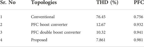
TABLE 2. Analysis of PF and THD.
Modulated signal controls the duty ratio of pulses. In the SVPWM technique, the voltages are represented by space vector in different sectors. Each voltage vector is the result of adjacent voltage vectors in that respective sector. There are five major steps in SVPWM control configuration. This strategy starts with the calculation of phase angle and reference voltage magnitude based on the supply voltage. The next step is to determine the modulation index. In the third step, sector number is calculated from a sector angle. The fourth step is calculation of T1, T2, and T0. In the final step, modulation time of switching states is calculated (Tran, 2012). In SVPWM, eight switching patterns are utilized for approximated reference voltage vectors to find sectors (Mahendran, 2013). In motor drive applications, SVPWM is used to control switching the inverter for DC to AC conversion. This reduces the THD of the input current applied to the motor (Ramos-Paja et al., 2022). Its DC bus voltage usage efficiency is 90.6%, 15.5 times greater than SPWM (Devices, 2000). Over modulation based SVPWM was suggested by Holtz in 1991, which further increased the DC bus efficiency (Holtz et al., 1993; Quan, 2011).
As part of the work, a BLDC engine was built and examined. Variants of the motor power supply and various sensors for determining the angular position of the motor shaft were tested. The tests used a three-phase electronic commutator bridge system with an optional DC/DC converter and an electronic commutator system. Both of these systems were designed and created as part of our research work. A schematic of the test stand with the installed measuring infrastructure is shown in Figure 1.
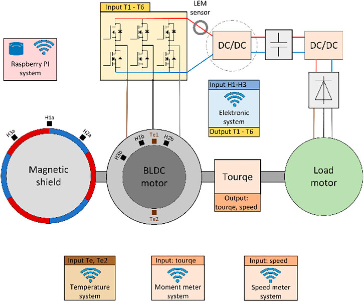
FIGURE 1. Scheme of the construction of the BLDC engine.
The developed research stand allows us two options for powering the engine. In the first option, the transistors of the electronic commutator bridge are actuated only on the basis of unmodified signals provided by the rotor angular position sensors. In the second option, the transistors of the electronic commutator bridge are actuated on the basis of the signal from the shaft position sensors modified by the PWM signal. Examples of the control voltage waveforms (orange) fed to the transistor gate and the voltage on the motor windings (blue) in the case of both power supply variants are shown in the oscillograms in Figure 2. The waveforms for the variant with DC/DC converter are on the left, and the waveforms generated when the drive signal of the bridge transistors is modified by the PWM signal are shown on the right.
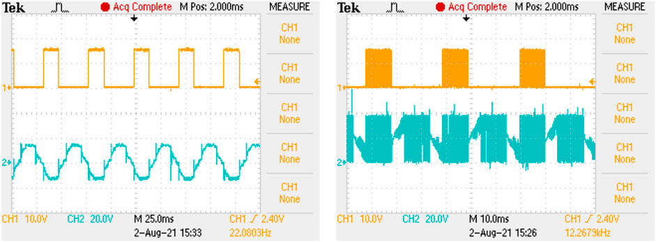
FIGURE 2. Oscillograms showing the control signal of the bridge transistor (left) and the output voltage of the transistor for BLDC motor control with and without PWM (right).
It is possible to change the average value of the voltage supplied to the motor windings, which allows the motor rotational speed to be regulated by changing the PWM signal duty cycle. Additionally, the duty cycle of the PWM signal enables the implementation of the current limiting function. In the first variant of the power supply, the adjustment of the engine speed and the current limitation function were performed with an additional DC/DC converter indicated via a broken circle in the diagram in Figure 2. In both cases, the current limitation is based on the value of the current consumed by the electronic commutator bridge, measured with the LEM sensor.
Our measuring system uses sensors that provide an analog signal at the output (a signal from thermistors representing temperature and another signal representing the load torque) or a digital signal (from hallotrons, and rotational speed signal from a torque meter).
2 Proposed modified Zeta converter fed BLDC motor drive
Figure 3 shows the basic circuit of a proposed modified Zeta converter fed BLDC motor drive. A BLDC motor drive encounters serious power quality problems. To reduce losses due to low power factor, suitable PFC converters are designed. These converters are typically categorized into two major classes based on conduction mechanisms, which are either discontinuous conduction mode (DCM) or continuous conduction mode (CCM). Both techniques are considered good based on the environment in which they are used. CCM has low switching losses as it requires a lower switching frequency, but it has a complex control consisting of two control loops and three sensors (Holtz et al., 1993; Quan, 2011). DCM is suitable for low filtering (LF) applications as it requires only one control loop and a single voltage sensor for DC link voltage control (Holtz et al., 1993; Quan, 2011). DCM offers increased losses due to high fsw.
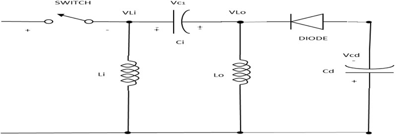
FIGURE 3. Basic circuit of modified Zeta converter.
2.1 Operation of the improved modified Zeta converter
In DICM, the current flow is not continuous into the output inductor in a cycle. The modified Zeta converter operates on DICM to improve the power factor in the BLDC motor drive. The complete DICM operation of the modified Zeta converter can be divided into four major modes, as explained below.
2.1.1 Mode 1
This mode starts with turning ON switch Sw. As the switch turns ON, the charge starts building up across intermediate capacitor Ci, input inductor Li, and output inductor Lo, as shown in Figure 4. Mode 1 is divided into two parts. In the first part, voltage is increasing across the intermediate capacitor due to negative charging of the capacitor. During this mode, diode D is reverse biased, and load is applied to the Cdc directly. DC link capacitor voltage discharges through the load in this mode. In the second part of mode 1, the intermediate capacitor starts charging up in a positive direction, as shown in Figure 4. The intermediate capacitor voltage (Ci), output inductor current (iLi), and output inductor current (iLo) continue rising. The duration of this mode depends upon duty ratio and is usually 15%–25% of the switching period.
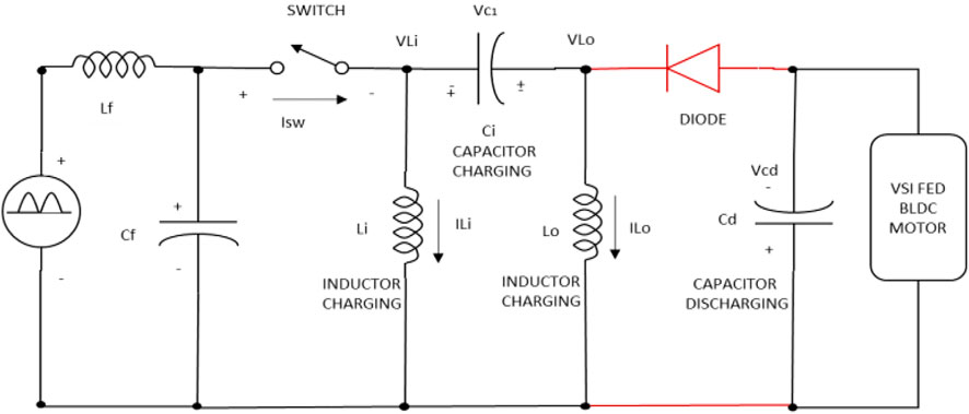
FIGURE 4. Mode 1 of modified Zeta converter.
2.1.2 Mode 2
This mode begins with turning OFF switch Sw. In this mode, Ci discharges according to Figure 5. As intermediate capacitor voltage is reduced, output inductor current decreases and input inductor current keeps increasing. A diode is forward biased and starts conducting. DC link capacitor charges through this diode; thus, voltage across the DC link capacitor starts increasing. Figure 5 shows that addition of the input inductor current (iLi) and output inductor current (iLo) results in the diode current (iD). This mode ends when the DC link capacitor charges up to voltage equal to the intermediate capacitor voltage (VCi).
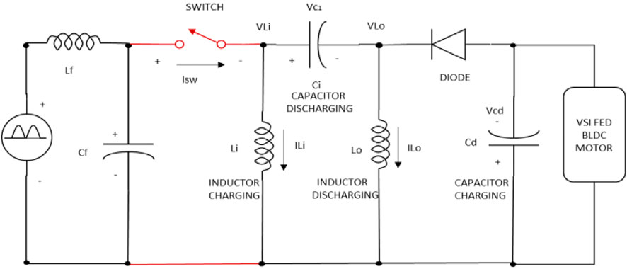
FIGURE 5. Mode 2 of modified Zeta converter.
2.1.3 Mode 3
This mode starts when the intermediate capacitor further discharges through the input and output inductor, and VCi declines from VDC. In this mode, DC link voltage rises as the DC link capacitor charges and, as the diode is forward biased, the output inductor discharges through it. The voltage across the DC link capacitor increases, the current through the output inductor decreases, and the current through the input inductor continues to increase. As the modified Zeta converter is meant to function in DICM, the current through the output inductor lowers to zero in mode 3. The output inductor is intended to be discharged entirely, which requires the output inductance to be lower in value than the input inductance. The total duration of modes 2 and 3 is 20%–30% of one switching time period. Mode 3 is presented in Figure 6.

FIGURE 6. Mode 3 of modified Zeta converter.
2.1.4 Mode 4
This mode starts with polarity reversal of output inductor current after reaching zero. This mode is also divided into two parts. In the first part of the mode input inductor, the current increases as the intermediate capacitor continues discharging. During that interval, the diode is reverse biased, and the output inductor current is equal in magnitude to the inductor current. The magnitude of Vdc reduces as the Cdc discharges directly through load.
The second part of the mode starts by the time the intermediate capacitor voltage becomes zero. After this, the intermediate capacitor charges up with reverse polarity. The input inductor voltage drops down, and the input inductor current to charge Ci is shown in Figure 7. Mode 4 is usually the longest of all modes. It generally takes 50%–70% of the time of a complete cycle. The cycle then repeats itself when switch Sw is again turned ON.
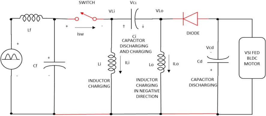
FIGURE 7. Mode 4 of modified Zeta converter.
3 Proposed model
The proposed architecture of the BLDC motor drive is shown in the diagrams above. A single-phase voltage source was used and an uncontrolled semiconductor diode bridge rectifier was used to convert sinusoidal AC into pulsating DC. This pulsating DC voltage source involves ripples due to full-wave rectification operation. LC filters were utilized to minimize the ripple factor to achieve a constant DC supply. This filtered DC supply was applied across the input of the modified Zeta converter. The modified Zeta converter comprises a MOSFET switch controlled by PWM pulses, an Li, an Lo, a Ci, and a Cdc. When the MOSFET switch is turned ON, the input inductor, intermediate capacitor, and output inductor start charging. During this interval, the diode is in the non-conduction mode as it is reverse biased according to configuration. The load was applied by the attached Cdc. As the switch is turned OFF and the DC link capacitor discharges to the lower voltage, the diode becomes a forward biased intermediate capacitor. In this way, a single voltage loop was used to control the Vdc of the modified Zeta converter. The DC link voltage was supplied to a voltage source inverter (VSI). A VSI is a three-leg semiconductor switch-based bridge. Six insulated-gate bipolar transistor (IGBT) based switches were used in VSI design configuration. S1, S3, and S5 make up the upper legs, and S2,S4, and S6 configure the respective lower legs, as shown in the diagram. Switches were numbered based on the switching sequence. In this switching sequence, S2 was switched ON after S1, and S3 was triggered ON after S2. There is a gap of 60° between any switching. S1and S2 make up the first leg, and their common junction point provided one phase of a three-phase output supply. The next two legs provided the other two phases. Two switches of a leg are toggle switches. If the upper switch is ON, the respective lower switch must be OFF, and vice versa. When the upper switch was ON and the lower switch was OFF, a positive half cycle of the respective phase was supplied to the load, and the reverse was needed for the negative half cycle. The next respective upper and lower switches were triggered in the same manner, with a gap consisting of a 120° phase shift. In this manner, a three-phase output voltage supply was attained with a
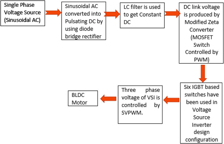
FIGURE 8. Block diagram of proposed model.
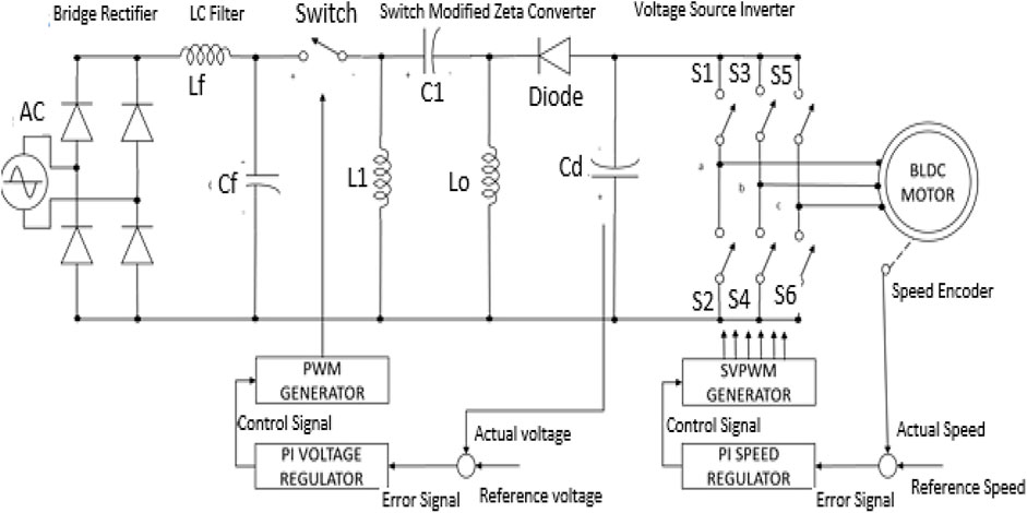
FIGURE 9. Proposed model of power factor correction.
4 Boost converter
Boost converter technology for PFC is not complex, yet not typical, and allows low distorted current for input, with the power factor of almost unity, by means of the numerous categories of devoted methods in the Simulink system. These methods were employed with average current mode control, peak current control, and hysteresis control in supply. As the purpose of this study, modern on-cycle control and self-control technology were employed for power factor increase of a power supply for any system.
Boost converter is a category of power converter that gives a DC output voltage that is higher than the input supplied to the converter; it can also be considered a category of switching mode power supply (SMPS). The boost converter can be manufactured in different configurations, but the basic construction must contain a minimum of two semiconductor switches (normally a transistor and a diode) and should also have one energy storing component. A boost converter has good self PFC (Vijayarajeswaran, 2012). Figure 10 shows the PFC boost converter Simulink model.
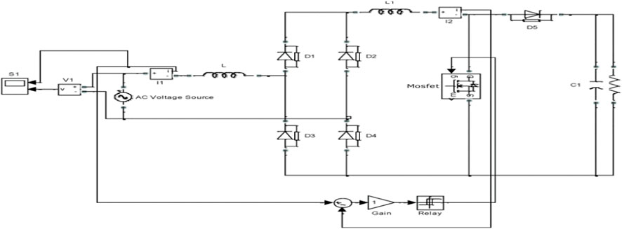
FIGURE 10. PFC boost converter Simulink model.
4.1 PFC double boost converter
Double boost, as the name suggests, must have two boost converters connected in parallel. Two or more boost converters are involved, which are associated in parallel and function at the same switching frequency. This double boost converter diminishes the PFC total switching loss and increases line current quality. Due to different switching frequency values and current amplitudes, double boost diminishes the switching losses for two switches. Modeling, simulation, and results of the PFC double boost converter are shown in Figure 11.
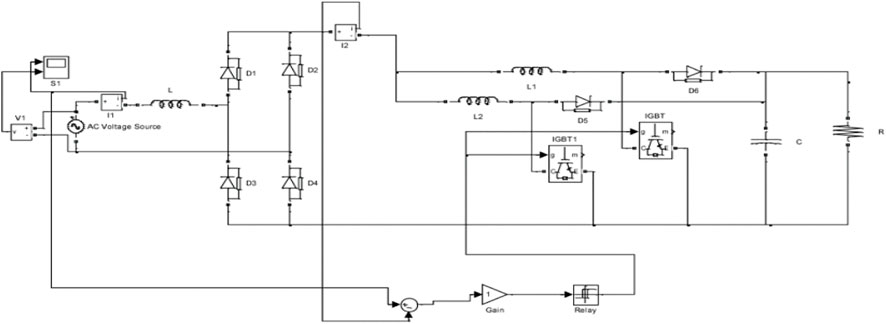
FIGURE 11. PFC double boost converter Simulink model.
5 Simulation
The proposed BLDC motor drive was simulated in MATLAB/Simulink. A screenshot of the simulation model is shown in Figure 11. A 220 V 50 Hz supply was used as an AC voltage source. Four diodes were used to design a full bridge rectifier for rectification of the input AC source. The model provided a pulsating output voltage with ripples. An LC filter was designed to produce smoother output DC. An inductor with an inductance value of 1.6 nH and a capacitor with capacitance value of 330 nF were used as Lf and Cf. The output of the LC filter was supplied to the modified Zeta converter. Li, Lo, and Ci were charged through MOSFET acting as a switch. The modified Zeta converter was designed to operate in DICM, which demands a discontinuous current through Lo, even for the worst switching cycle. For this purpose, the value of Lo was chosen to be a much lower inductance compared to Li. It was set at 70 mH while the suitable value of input inductance is 3.3 mH, even at minimum voltage supply and maximum ripple current. An intermediate capacitor Ci with a capacitance value of 0.66 µF was used, as it is desired to have low ohmic and equivalent series resistance (ESR) for high frequency switching and surge currents. The DC link capacitor was charged through a diode. A 2200 µF capacitor was used as DC link capacitor Cdc, as a higher capacitance is required for reduced ripples on high current and switching frequency values. A voltage follower control was designed to control the output of the modified Zeta converter. The V was compared with the step signal acting as a reference voltage value that fed the PI controller’s error signal. The PI controller fed a control signal to the PWM generator with 5000 Hz switching frequency to generate pulses accordingly. The PWM generator pulses were fed to the MOSFET switch of the modified Zeta converter. The DC link output voltage was supplied to the VSI as an input. Six MOSFET switches were used to design the VSI. SVPWM triggered the MOSFET switches to produce the three-phase alternating output voltage. The output of the VSI was fed to the BLDC motor as a supply to the three-phase armature winding. The output parameters extracted from the BLDC motor were stator current of phase a (Is-a), rotor speed in radian per second further converted to revolutions per minute (RPM), and electromagnetic torque (Te) in Nm. The output parameters were connected to the scope for waveform display.
The speed output parameter of the BLDC motor was compared with the step input taken as a reference speed value to get an error signal, which was then fed to the PI controller. The PI controller produced a speed control signal, which was fed to the SVPWM generator as the magnitude of the reference vector. The output of the SVPWM generator was de-mux and supplied to respective switches. A sub-block of the PF calculator was used to calculate the power factor of input supply by taking the cosine of the phase difference in input current and voltage. Similarly, the PF of the output supply of the VSI was calculated, then both were compared in output scope. The RMS function blocks of Simulink were introduced to calculate the root mean square values of power factor across input and output. The real-time power factor values throughout the simulation were displayed across the scopes. A function block of THD was utilized across the input source current to calculate the distortion of the supply current. Here, the supply frequency was taken as 60°. The voltages and currents of the simulated model was connected to scope through GOTO tags. A Powergui block was inserted by setting the sample time to 0.5 µs to complete the simulation model. Figure 12 shows the MATLAB/Simulink model of the proposed idea.
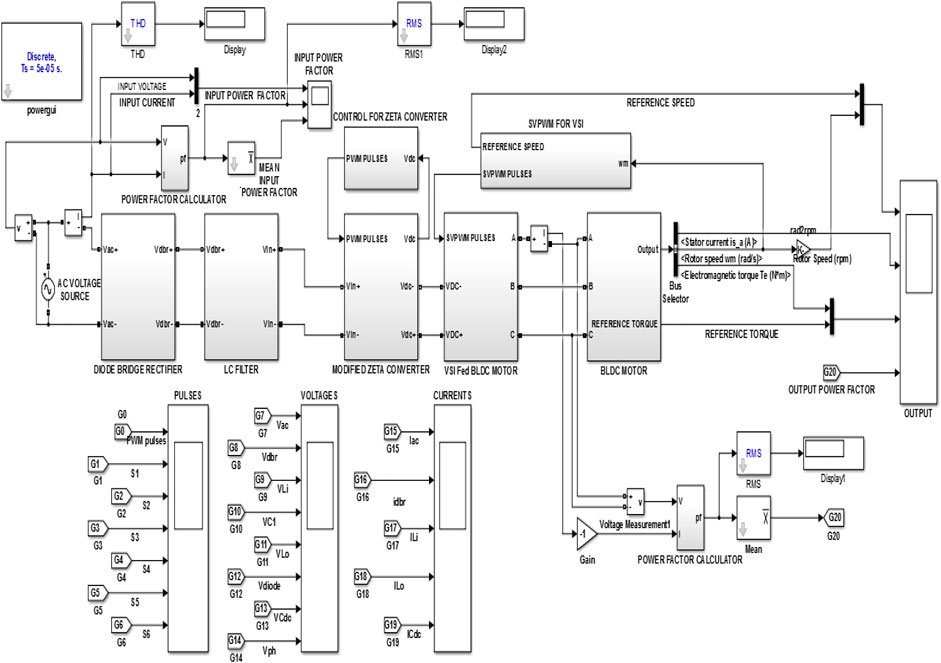
FIGURE 12. MATLAB/Simulink model of the proposed idea.
The following assumptions were made for the simulation of the proposed concept.
1) The components used in the simulation model are considered ideal, so there are no losses, and output power is equal to the power supplied.
2) The inductors used in the design, Li and Lo, are considered ideal, with RLi = RLo = 0. It is assumed there is no saturation problem.
3) The inductors used in the model are considered ideal, with ESR = 0 for both Ci and Co
4) The switching period is considered negligible as compared to a time constant of charging and discharging.
5) The MOSFET switches are considered ideal, with no switching losses.
These five assumptions were taken into account when interpreting the results of the simulation.
6 Results and discussion
The results of the simulation model are shown in Figure 13–16. Figure 13 shows the PWM pulses, which were fed to the MOSFET, acting as a switch. The pulses were generated from the PWM generator block of Simulink. The pulses were generated based on duty cycle. The PI controller decided the duty cycle per the error signal generated by the reference and DC link voltages. The controller functioned to reduce the error signal by closed-loop single voltage sensor-based control. The PWM signal was generated to raise the voltage to the reference voltage applied. In the simulation, the reference voltage was set at 200 V. The voltage waveforms of the proposed idea are shown in Figure 14. The figure shows that the DC link voltage continued rising until it reached the desired value. Once the reference value was achieved, a fixed and fluctuation-free voltage was obtained. This constant ripple-free voltage is the key to the PFC based BLDC motor drive. It provided a constant DC link voltage, as shown in the voltage waveform of Figure 15. When fed to the VSI, this DC link voltage generated an output AC supply with increased PF. The output parameters of the BLDC motor drive are shown in Figure 16. The three-phase output from the VSI was attained when controlled by Hall sensors. The stator current of phase a is shown, which demonstrates the sinusoidal nature of the output power supply. The output phase voltage waveform of the VSI is shown in Figure 14, which is again sinusoidal. The speed of the BLDC motor in RPM is shown in Figure 16. The speed follows the reference speed provided. The electromagnetic torque of the BLDC motor is also shown. The output power factor is visible in this figure, which demonstrates the power factor improvement by the proposed scheme.
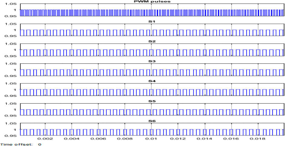
FIGURE 13. PWM pulses of BLDC motor drive.
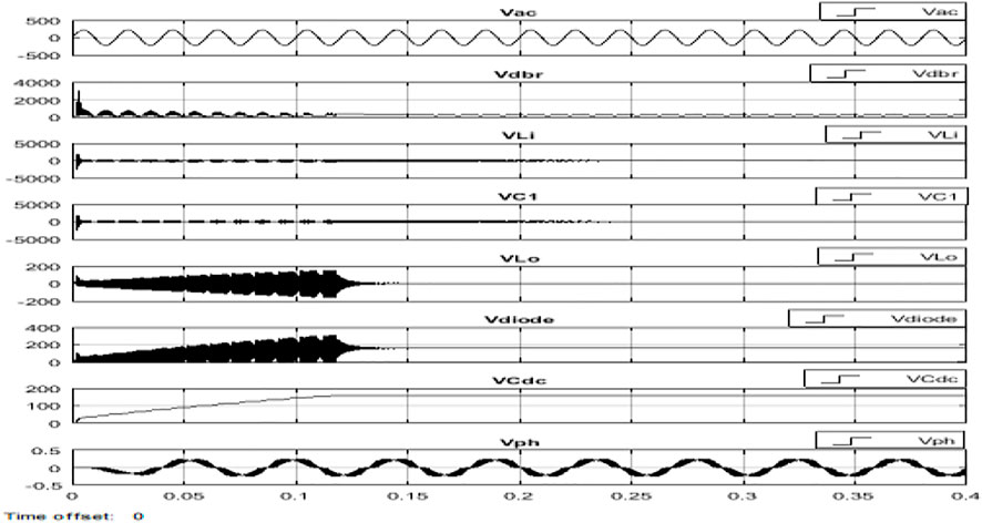
FIGURE 14. Voltage waveforms of BLDC motor drive.
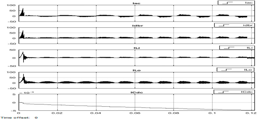
FIGURE 15. Current waveforms of BLDC motor drive.
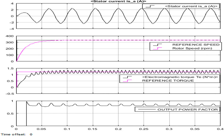
FIGURE 16. Output parameters of BLDC motor drive.
Our data indicate that the PFC modified Zeta converter has excellent power factor correction capability. The PFC double boost converter technology is better than the boost converter, which has also improved the power factor and reduced the THD in current supply. The PFC modified Zeta converter topology provides a power factor of 0.981, which is better than other topologies, and a THD of only 9.81%, which is also the best among all three topologies. Additionally, both of these components of the power supply can be further improved by applying other soft computing techniques.
7 Conclusion
This research demonstrates the design and simulation testing of a PFC and THD reduction-based BLDC motor drive. The design is cost-effective and provides wide-range speed control. A modified Zeta converter was used to reduce the power quality problems created by the rectification process. It is modified to operate in DICM to get a constant DC link voltage. This configuration improves the power factor. A simple DC link voltage follower control is utilized for a modified Zeta converter. The DC link voltage fed to the VSI generates AC output, which then runs the BLDC motor. An SVPWM controlled electronic commutation was used for the BLDC motor drive. This reduces mechanical losses and sparking due to the absence of brushes. It also reduces electrical losses and distortions. The performance of the proposed drive configurations was evaluated using the MATLAB/Simulink environment. The PFC modified Zeta converter topology has produced the best power factor of 0.981, which is better than other current topologies. The THD, at 9.81%, is also the lowest of all three topologies, which demonstrates the significance of the proposed model for use in low power and low-cost applications.
Data availability statement
The original contributions presented in the study are included in the article/Supplementary Materials, further inquiries can be directed to the corresponding author.
Author contributions
HAM, MS, MMH, and ZA: conceptualization, methodology, software, writing original draft; LB, HAM, MA: writing—review and editing; MZ and HAM: data curation; ZA: writing—review and editing. All authors have read and agreed to the published version of the manuscript.
Conflict of interest
The authors declare that the research was conducted in the absence of any commercial or financial relationships that could be construed as a potential conflict of interest.
Publisher’s note
All claims expressed in this article are solely those of the authors and do not necessarily represent those of their affiliated organizations, or those of the publisher, the editors and the reviewers. Any product that may be evaluated in this article, or claim that may be made by its manufacturer, is not guaranteed or endorsed by the publisher.
References
Aktaibi, A., Rahman, M., and Razali, A. (2010). A critical review of modulation techniques. Available at: http://www.academia.edu/3077823/A_Critical_Review_of_Modulation_Techniques.
Chao, K. H., Chang, L. Y., and Hung, C. Y. (2022). Design and control of brushless DC motor drives for refrigerated cabinets. Energies 15 (9), 3453. doi:10.3390/en15093453
Cheng, L. (2002). “DSP-based variable speed motor drive with power factor correction and current harmonics compensation,” in Proceedings of the 35th Intersociety Energy Conversion Eng. Conf. and Exhibit (IECEC), Las Vegas, NV, USA, July 2000, 1394–1399. doi:10.1109/IECEC.2000.870956
Devices, A. (2000). Implementing space vector modulation with the ADMCF32X. Norwood, MA: Analog Devices Inc.
George, G. J., Rakesh, R., and Arun, N. (2012). “PMBLDC motor drive with power factor correction controller,” in Proceeding of the Int. Conf. on Computing, Electronics and Electrical Technologies (ICCEET), Nagercoil, India, March 2012, 63–68. doi:10.1109/ICCEET.2012.6203872
Gopalarathnam, T., and Toliyat, H. A. (2003). A new topology for unipolar brushless DC motor drive with high power factor. IEEE Trans. Power Electron. 18 (6), 1397–1404. doi:10.1109/tpel.2003.818873
Hicham, C., Nasri, A., and Kayisli, K. (2021). A novel method of electric scooter torque estimation using the space vector modulation control. Int. J. Renew. Energy Dev. 10 (2), 355–364. doi:10.14710/ijred.2021.33403
Holtz, J., Lotzkat, W., and Khambadkone, A. (1993). On continuous control of PWM inverters in the overmodulation range including the six-step mode. IEEE Trans. Power Electron. 8 (4), 546–553. doi:10.1109/63.261026
Hua, B., Zhengming, Z., and Meng Shuo, M. (2003). Comparison of three PWM strategies- SPWM, SVPWM & one-cycle control. Power Electron. Drive Syst. 2, 1313–1316. doi:10.1109/PEDS.2003.1283169
Khalkhali, H., Oshnoei, A., and Anvari-Moghaddam, A. (2022). Proportional hysteresis band control for DC voltage stability of three-phase single-stage PV systems. Electronics 11 (3), 452–515. doi:10.3390/electronics11030452
Khan, H. R., Kazmi, M., Bin Ashraf, H., Hashir Bin Khalid, M., Hasan, A., and Qazi, S. A. (2021). An isolated power factor corrected cuk converter with integrated magnetics for brushless dc ceiling fan applications. Electronics 10 (14), 1720–1724. doi:10.3390/electronics10141720
Lee, J., and Sun, Y. (1988). A new SPWM inverter with minimum filter requirement. Int. J. Electron. 64 (5), 815–826. doi:10.1080/00207218808962856
Madani, S. M., Lei, H., and Toliyat, H. A. (2002). “A low-cost four-switch BLDC motor drive with active power factor correction,” in Proceedings of the 28th Annual IEEE Conf. of Ind. Electron. Society (IECON), Seville, Spain, November 2002, 579–584. doi:10.1109/IECON.2002.1187572
Mahendran, N. (2013). Fuzzy controller based space vector pulse width modulation scheme for direct ac conversion system. Tamil Nadu India: Anna Univ. Available at: http://shodhganga.inflibnet.ac.in/handle/10603/10150 Thesis, E. E.
Martins, D. C. (1996). “Zeta converter operating in continuous conduction mode using the unity power factor technique,” in Proceedings of the 1996 Sixth International Conference on Power Electronics and Variable Speed Drives (Conf. Publ. No. 429), Nottingham, UK, September 1996, 7–11. doi:10.1049/cp:19960879
Niculescu, E., Niculescu, M. C., and Purcaru, D. M. (2008). “Modelling the PWM Zeta converter in discontinuous conduction mode,” in Proceedings of the 14th IEEE Mediterranean Electrotechnical Conf. (MELECON 2008), Ajaccio France, May 2008, 651–657. doi:10.1109/MELCON.2008.4618509
Ponder, A., and Pham, L. (2010). “Performance evaluation of space vector modulation controlled inverter fed variable speed wind generator during permanent fault,” in Proceedings of the IEEE XIX International Conference on Electrical Machines (ICEM), Rome Italy, September2010, 6–8. doi:10.1109/ICELMACH.2010.5607826
Quan, H. (2011). “Study of a novel over-modulation technique based on space-vector PWM,” in Proceedings of the IEEE Computer Distributed Control and Intelligent Environmental Monitoring (CDCIEM), Changsha, China, February 2011, 295–298. doi:10.1109/CDCIEM.2011.187
Ramos-Paja, C. A., Saavedra-Montes, A. J., and Bastidas-Rodriguez, J. D. (2022). Co-design of the control and power stages of a boost-based rectifier with power factor correction depending on performance criteria. Computation 10 (4), 61. doi:10.3390/computation10040061
Rashid, M. H. (2006). “Power electronics handbook: Devices,” in Circuits and applications (Massachusetts, MA, U S: Academic Press), 19, 525–530.
Singh, B., and Chaturvedi, G. D. (2008). Analysis, design, modeling, simulation and development of single-switch AC-DC converters for power factor and efficiency improvement. J. Power Electron. 8 (1), 51–59.
Singh, B., and Singh, S. (2010). Single-phase power factor controller topologies for permanent magnet brushless DC motor drives. IET Pwr. Electr. 3 (2), 147–175. doi:10.1049/iet-pel.2008.0313
Singh, S., and Singh, B. (2012). A voltage-controlled PFC Cuk converter based PMBLDCM drive for air-conditioners. IEEE Trans. Ind. Appl. 48 (2), 832–838. doi:10.1109/tia.2011.2182329
Singh, S., and Singh, B. (2010). “Voltage controlled PFC Zeta converter based PMBLDCM drive for an air-conditioner,” in Proceedings of the Int. Conf. on Industrial and Information Systems (ICIIS), Mangalore, India, 29 July 2010–1 August 2010, 550–555. doi:10.1109/ICIINFS.2010.5578643
Suti, A., Di Rito, G., and Galatolo, R. (2022). Novel approach to fault-tolerant control of inter-turn short circuits in permanent magnet synchronous motors for UAV propellers. Aerospace 9 (8), 401. doi:10.3390/aerospace9080401
Tran, P. (2012). Matlab/Simulink implementation and analysis of three pulse-width-modulation (PWM) techniques. M.S. thesis. Boise, Idaho: Boise St. Univ.
Keywords: voltage source inverter, brushless DC motor, modified Zeta converter, space vector pulse width modulation, discontinuous inductor current mode
Citation: Bin L, Abdeen Zu, Abrar M, Abdul Muqeet H, Shahzad M, Zulfiqar M and Hussain MM (2023) A novel approach to design of a power factor correction and total harmonic distortion reduction-based BLDC motor drive. Front. Energy Res. 10:963889. doi: 10.3389/fenrg.2022.963889
Received: 08 June 2022; Accepted: 26 September 2022;
Published: 10 January 2023.
Edited by:
Yiyi Zhang, Guangxi University, ChinaReviewed by:
Mohd Afroz Akhtar, Central Mechanical Engineering Research Institute (CSIR), IndiaSingaravelan Arumugam, Nitte Meenakshi Institute of Technology, India
Copyright © 2023 Bin, Abdeen, Abrar, Abdul Muqeet, Shahzad, Zulfiqar and Hussain. This is an open-access article distributed under the terms of the Creative Commons Attribution License (CC BY). The use, distribution or reproduction in other forums is permitted, provided the original author(s) and the copyright owner(s) are credited and that the original publication in this journal is cited, in accordance with accepted academic practice. No use, distribution or reproduction is permitted which does not comply with these terms.
*Correspondence: Muhammad Majid Hussain, bXVoYW1tYWQuaHVzc2FpbkBody5hYy51aw==