
95% of researchers rate our articles as excellent or good
Learn more about the work of our research integrity team to safeguard the quality of each article we publish.
Find out more
BRIEF RESEARCH REPORT article
Front. Energy Res. , 04 August 2022
Sec. Smart Grids
Volume 10 - 2022 | https://doi.org/10.3389/fenrg.2022.957825
This article is part of the Research Topic Emerging Boost Converter Topologies for Renewable Energy Applications View all 5 articles
 Saifullah Kakar1
 M. Saad Bin Arif1,2*
 Shahrin Md. Ayob1*
 Norjulia B. M. Nordin1
 Saad Mekhilef3,4,5
 Mehdi Seyedmahmoudian3
 Alex Stojcevski3
Multilevel inverters (MLIs) have seen significant growth in a variety of medium- to high-power industrial applications and have become a mature and viable solution for renewable energy systems over the past decade. The major concerns of MLIs are the high component count and the buck-type feature of the ac output voltage when used for grid-connected renewable-energy-based sources such as solar photovoltaic (PV) panels. As another option, a switched-capacitor (SC)-based inverter possessing the feature of boost ability is a prime solution to meet the requirements of ac power applications. Integrating an SC network with a neutral-point clamped (NPC) structure makes leakage current alleviation viable for transformerless PV grid-connected systems. In this article, an improved SCMLI based on the NPC structure is proposed to reduce the number of active switches and the number of switches in the charging loop, significantly reducing the power loss. It can generate seven voltage levels with voltage boosting and self-balancing of capacitors within a single-stage power conversion. The working principle of the proposed topology, circuit description, and control technique are presented. Further, the proposed inverter was compared with other recent SC topologies to show its superiority. In the end, a laboratory prototype was developed and tested for the seven-level module under steady-state and dynamic conditions to validate the practical viability of the proposed configuration. The proposed inverter’s maximum efficiency was 97.5% at 1.2 kW rated power.
Multilevel inverters (MLIs) have attracted increasing attention in renewable energy generation systems over the past decade (Iqbal et al., 2020). Among all renewable energy sources, the use of photovoltaic (PV) systems in power generation has regularly increased worldwide. MLIs play a vital role in power conversion suitable for different applications owing to their promising features such as high efficiency and power density. In contrast to the classical two-level inverter, their main features are higher modularity and scalability, excellent output waveform quality, appropriate power density, and suitable cost (Kakar et al., 2021a; Kakar et al., 2021b; Iqbal et al., 2021). However, the major concerns of MLIs are the high component count and the buck-type feature of the ac output voltage when used for grid-connected renewable energy-based sources such as solar PV panels. Therefore, a separate boost dc–dc converter or transformer is imperative to boost the input dc voltage to an acceptable range, increasing the systems’ size, cost, weight, and losses.
Therefore, the switched-capacitor (SC) concept integrated into MLIs is an effective solution to boost the low input voltage obtained from renewable energy sources such as PV and fuel cells with multistepped voltage levels. The concept of a SC inverter was introduced first by Mak and Ioinovici in 1998 (Hussan et al., 2021). In general, SC-based MLIs require a single dc source and capacitors in place of dc sources and take advantage of the series–parallel technique to boost the low input voltage near the sinusoidal output voltage waveform. SCMLI is one of the popular MLI structures that can inherently balance the capacitor voltage and boost the input voltage simultaneously. Therefore, the need for sensors, complex control techniques, and auxiliary circuits for balancing the capacitor voltage is completely avoided. However, SCMLIs require a large number of power switches and capacitors with high voltage stress. Thus, the overall system becomes complex and costly, and efficiency is reduced when high voltage levels are required. Therefore, several SCMLI topologies have been introduced over the years to reduce the number of circuit components (Taghvaie et al., 2017; Ali and Krishnasamy, 2018; Peng et al., 2019; Roy et al., 2019; Saeedian et al., 2019; Khan et al., 2020; Roy and Sadhu, 2020; Chen et al., 2021; Lin et al., 2021; Roy et al., 2021). However, these topologies share a common drawback of high common-mode voltage (CMV) that induces leakage risk, making these topologies less viable for transformerless PV grid-tied systems. An alternative solution is to employ neutral-point clamped (NPC) inverters that maintain the CMV constant; thus, mitigating the leakage current to an acceptable range. In addition, power quality increases by enhancing the number of output voltage levels. In this category, inverter structures like active neutral-point clamped (ANPC) (Wang et al., 2017), T-type (Saeedifard et al., 2011), and flying capacitor (FC)-based (Siwakoti et al., 2019a) are the most developed and efficient topologies. In addition, other two of the main issues involving the ANPC and NPC topologies discussed above are the lack of voltage-boosting capability and the capacitor’s voltage unbalancing.
On this line, several attempts have been made in literature by integrating SCs into an NPC structure to achieve voltage boosting, which successfully solved the voltage unbalancing and boosting issues in ANPC topologies and the CMV in other topologies discussed above. In recent years, two 5-level boost T-type ANPC inverters were developed by Rech (2019) and Siwakoti et al. (2019b) to generate voltage levels of 0, ±0.5 Vin, and ±1 Vin. The one by Rech (2019) had a similar structural layout to the classical five-level ANPC, but both switches (S5 and S6) were connected in reverse. Because of this, the capacitor implemented in this topology was actually an SC rather than a FC. The second topology by Siwakoti et al. (2019b) was also constructed on the SC concept, and two switches were less used than the first one. However, their main drawback was that two switches (S3 and S6) in each topology needed to block a bipolar voltage so that active and reactive powers could not conduct through them simultaneously for some levels. Hence, a special control strategy was necessary for nonunity power factor (FP) operation, as analyzed by Siwakoti et al. (2019b). In addition, the switch count was high in these topologies for the five-level inverter. To resolve the drawbacks of the topologies in the study by Rech (2019) and Siwakoti et al. (2019b), Ye et al. (2021) developed a new five-level inverter by inserting an SC unit into the classical three-level NPC inverter phase leg. The SC unit comprised two SCs and one bidirectional switch. However, it had no boost capability. The topology presented by Lee et al. (2019a) could produce up to seven voltage levels, with a gain factor of 1.5.
To further improve voltage boosting, a dual T-type seven-level topology (Lee and Lee, 2019) was attempted. The achieved boosting gain of this topology was 1.5 at the cost of incorporating more power switches and floating capacitors. Another topology (Lee et al., 2019b) preserved the two advantages of the high voltage-boosting gain of 1.5 and the seven voltage level generation in the study by Lee and Lee (2019) while achieving low switch count and guaranteeing low voltage stress on the switching devices. The topology by Sathik et al. (2019) was developed with the intent to reduce the voltage stress on switches and the number of capacitors while offering the same benefits of 1.5 boosting gain. Another attempt was made by Sandeep et al. (2020) to improve the topology presented by Lee and Lee (2019) in terms of switch count and voltage stress reduction. Similar features could also be noticed from the seven-level SC topology by Zeng et al. (2019). The inverter by Siwakoti (2018) was a first attempt that enhanced the boosting gain to unity. Inspired by the ANPC topology presented by Siwakoti (2018), two new enhanced ANPC topologies were derived by Lee et al. (2019c), where a higher voltage gain and switch reduction were achieved.
However, NPC-type topologies suffer from drawbacks such as a significantly large number of switches in the load current path (Npath) and the number of switches in the charging loop (Npath, C). In recent years, a new topology proposed by Lee and Lee (2020) resolved these issues by extending the charging duration of SCs. The topology is termed switched-capacitor-based modular T-type inverter (SC-MTI). This significantly reduced the capacitor voltage ripples but at the expense of a high switch count. This article proposes an improved seven-level SCMLI that retains the main features of SC-MTI with additional improvements such as the following:
• Reduced the number of active power switches by four for seven-level voltage waveform generation.
• Only a single switch and a diode are utilized to charge each capacitor during all states of inverter operation.
• A lower number of switches in load current conduction and SC charging paths.
• The current flow among SCs is restricted. This is a benefit because the charging current only flows from the dc-link capacitor to the SCs.
Figure 1A shows the seven-level bipolar circuit configuration of the proposed NPC topology. It comprises 12 switches with antiparallel diodes, four diodes, and four switched capacitors to generate seven equal voltage levels of the following amplitudes: +0.5 Vin, +1 Vin, +1.5 Vin, −0.5 Vin, −1 Vin, −1.5 Vin, and 0 Vin. It is a combination of an SC module and a T-type inverter. The SC module comprises basic SC units between the dc-link network and a T-type unit. In the proposed topology, the positive pole generates positive voltage levels and the negative pole is responsible for generating the negative voltage levels at the load. Each pole uses separate paths for the charging process. It is noteworthy that the capacitors can be charged for at least the half-cycle of the operation, and the capacitors will remain in a charging state when not delivering power to the load. The operation of the seven-level inverter is shown in Figures 1B–H. Here, the path for carrying load current is indicated by red, blue dotted lines indicate the charging paths for switched capacitors, and the green line indicates freewheeled current in reactive mode. In this analysis, all power switches and diodes are assumed to be ideal, neglecting their on-state resistance and forward voltage drop. In addition, the SC voltage ripples are neglected by assuming large capacitors. Further, the generation of seven voltage levels based on the switching states of the proposed inverter is listed in Table 1. Here, “1” and “0” represent a switch’s “ON” and “OFF” states, respectively. In contrast, “C” and “D” represent the charging and discharging of the SCs.
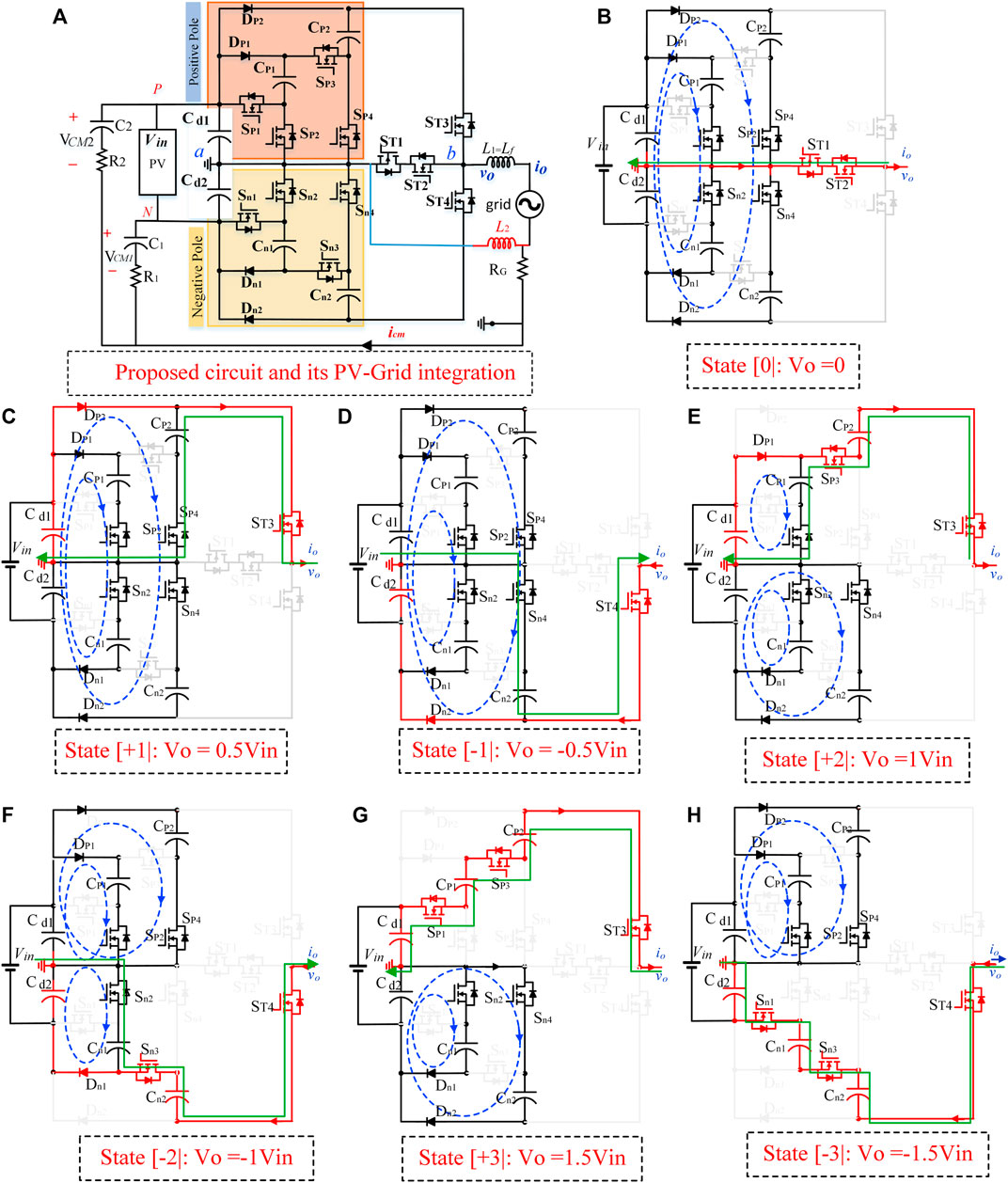
FIGURE 1. Circuit configuration, photovoltaic grid integration, and modes of operation of the proposed circuit.
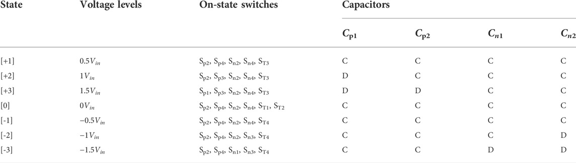
TABLE 1. Switching states for the proposed seven-level inverter.
As detailed in Figure 1 and Table 1, both the inverter structure and operation of the proposed SCMLI are symmetrical. The capacitors in the positive pole are responsible for the positive half-cycle and the capacitors in the negative pole are responsible for the negative half-cycle of the output waveforms. For both unity power factor and nonunity power factors, the functions and operations of the involved capacitors are the same and are able to handle the same amount of power. Hence, all capacitor voltages in the circuit are naturally balanced at their rated values. Moreover, the upper SCs and lower SCs are connected in parallel with the dc-link capacitors for the positive and negative half-cycle levels, respectively. Therefore, their voltages can be self-balanced to the same magnitude as the dc-link voltage of 0.5 Vin.
To find the value of the capacitors, their longest discharging periods in a complete cycle must be evaluated for a permissible voltage ripple.
Therefore, by integrating the load current from ton to toff, the maximum amount of electric charge (ΔQC) discharged by each capacitor to the load can be expressed as follows.
where Io represents the load current, fo is the output frequency, φ is the phase angle, and [ton−toff] are the start and end instants of the capacitor discharging duration.
Therefore, considering the minimum voltage ripple (ΔV), the optimum capacitance of the capacitors can be obtained as
where
A detailed CMV and leakage current analysis of the proposed seven-level circuit configuration has been conducted in this section (Xiao, 2020). The equivalent circuit is drawn in Figure 1A. While, P and N represents input terminals of the input dc source (i.e., PV arrays), respectively. Whereas Va,N and Vb,N are the output voltages of the proposed inverter relative to the N terminal of the PV. Here, a and b are the output terminals of the differential mode voltage (VDM), and C1 and C2 are photovoltaic (PV) parasitic capacitors against the ground. Considering parasitic C1 for analysis, it is clear from Figure 1A that Vb, N = 0.5 VC and Va, N for all switching states can be derived using Kirchhoff’s voltage law according to the operating modes of the seven-level inverter and operating state of the switches tabulated in Table 1.
Taking point N as the reference, CMV (VCM) and differential mode voltage (VDM) are expressed as follows:
Both the CMV and DMV that contribute to the total CMV (VCM, T) can be expressed using the equation below
where L1 and L2 are the filter inductors at the ac side.
While the leakage current (iCM) is mainly induced by the fluctuation of CMV as expressed in Eq. 8.
It shows that the flow of the ground leakage current through the parasitic capacitance (C) is dependent on the behavior of CMV. In case CMV transitions occur at high frequency, it will introduce a large leakage current. Therefore, to minimize or eliminate the common-mode leakage current, it is necessary for CMV to be kept constant.
Assuming that the L1 = Lf and L2 = 0, then
By putting the values obtained from Eq. 3 to Eq. 6 in Eq. 9, the total CMV values for different switching states can be obtained. From this analysis, it is clear that the variation of the CMV remains constant at 0.5 VC at each switching for the proposed seven-level circuit topology. Therefore, the proposed topology naturally maintains the total CMV constant at 0.5 VC because of the dc-link capacitor bridge arm. A similar procedure can be applied when considering parasitic capacitors (C2) and VCM2. The equivalent CM circuits can be derived, but here, Vb, N = −0.5, and the variation of the total CMV (
This study conducts a comparative investigation with the SC-MTI (Lee and Lee, 2020) chosen as the benchmark reference and other state-of-the-art topologies for comparison. To evaluate the implementation cost-per-level for each inverter, the cost function (CF) is calculated using Eq. 10. Here, β is the weight coefficient and is set to 0.5 for all topologies. Here, NS is equal to 1 for all inverters as single-source topologies are selected for comparison. Whereas
Compared to SC-MTI, the proposed inverter reduced the number of required active switches by four for seven-level generation. In addition, only a single active switch and a diode are utilized to charge any switched capacitor in the proposed topology, and there is no charge flow among the capacitors. Overall, the cost is minimized, and the efficiency of the proposed inverter topology is significantly improved. A comprehensive comparison analysis among state-of-the-art SCMLIs and the proposed SCMLI is illustrated in Table 2. The numbers of switches employed in the proposed topology are similar to those of the topologies presented by Khan et al. (2020), Barzegarkhoo et al. (2021), and He et al. (2021). Unlike many SCMLIs, however, owing to the reduction in the number of active switches, the reverse-power flow is not restricted by the proposed SCMLI, making it suitable for grid-connected renewable energy sources.
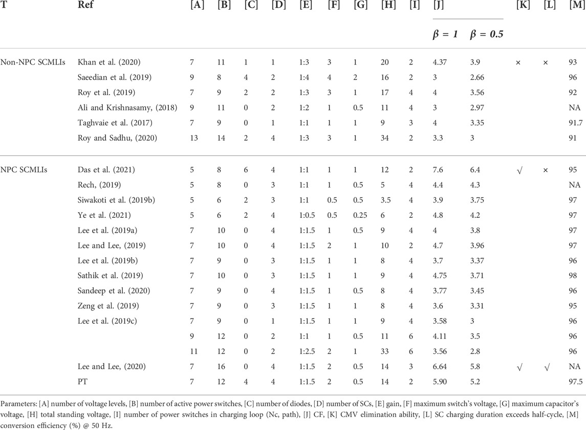
TABLE 2. Performance comparison with existing switched-capacitor-based multilevel inverters.
Although the gain of the proposed inverter is low (i.e., only 1.5 Vin for seven levels) compared to some other topologies, it provides other benefits such as lower voltage ripple, leakage current minimization, and single-source utilization. In addition, it uses a single switch and diode to charge each switched capacitor, and the switches in the charging path are more in SC-MTI. Also, the current flow among SCs is restricted because of its unique structure. In addition, it has the same ripple as the latest topology (Barzegarkhoo et al., 2021) while reducing the component count and conduction loss. In the topologies by Ali and Krishnasamy (2018), Peng et al. (2019), Roy et al. (2019), Saeedian et al. (2019), Khan et al. (2020), Chen et al. (2021), He et al. (2021), and Roy et al. (2021), because the neutral of the ac output is connected to a half-bridge or full-bridge, CMV is introduced. Therefore, their topological structures induce the risk of leakage current, making these SCMLIs less viable for photovoltaic (PV) applications. The lack of reactive power capability in nonunity reactive power mode is the main drawback of the topology (Saeedian et al., 2019). Hence, it is unsuitable for grid-connected renewable energy sources. As can be observed from Table 2, the inverter structures (Ali and Krishnasamy, 2018; Peng et al., 2019; Roy et al., 2019; Saeedian et al., 2019; Khan et al., 2020; Chen et al., 2021; He et al., 2021; Roy et al., 2021) require three dc sources for three-phase applications, unlike the proposed topology that needs only one dc source. To minimize power loss in SCMLIs, it is necessary to use a low number of switches in the different levels (Npath) and charging paths of SCs (Npath, c). For example, four and three switches are conducted in SC’s charging path for the SCMLIs proposed by Lee et al. (2019b), Sathik et al. (2019), Zeng et al. (2019), Sandeep et al. (2020), and Lin et al. (2021) and by Taghvaie et al. (2017) and Lee and Lee (2020), respectively. At the same time, only two switches are conducted in SC’s charging path for each SC in the study by Das et al. (2021) and Lee and Lee (2019). However, these inverters require more switches, and the discharging duration is higher than the charging duration.
In the laboratory, a seven-level inverter prototype was developed to verify the performance evaluation of the proposed topology. The input dc source voltage was set to 60 V, and 1200 μF capacitors were selected. To test the proposed topology operating at a low switching frequency, the nearest level control (NLC) modulation technique with dSPACE 1104 controller was used to generate gate signals for the power switches. The NLC method, also called the round modulation method or the half-integer method, can be easily performed by round function (Sathik et al., 2021; Mustafa et al., 2022; Siddique et al., 2022). This technique can produce the closest voltage level by comparing the inverter output voltage with the reference sinusoidal voltage to produce proper switching signals.
The experimental results obtained in the steady state of the inverter operation are presented in Figures 2A and B. Figure 2A shows the voltage and current frequency spectra of the output voltage considering pure resistant load (R = 200 Ω). Here, the output voltage and current seven-level staircase waveforms were obtained without using output filters. Meanwhile, its peak of fundamental output voltage reached nearly 90 V, which was 1.5 times that of the input voltage. The THD values of the output voltage and load current without filters were 16.5 and 16.1%, respectively. The corresponding output voltage waveform for the nonunity power factor with R = 100Ω and L = 200 mH, is shown in Figure 2B, as it can be observed that the SCs (Cp1 and Cn1) were balanced at approximately 30 V in the steady state.
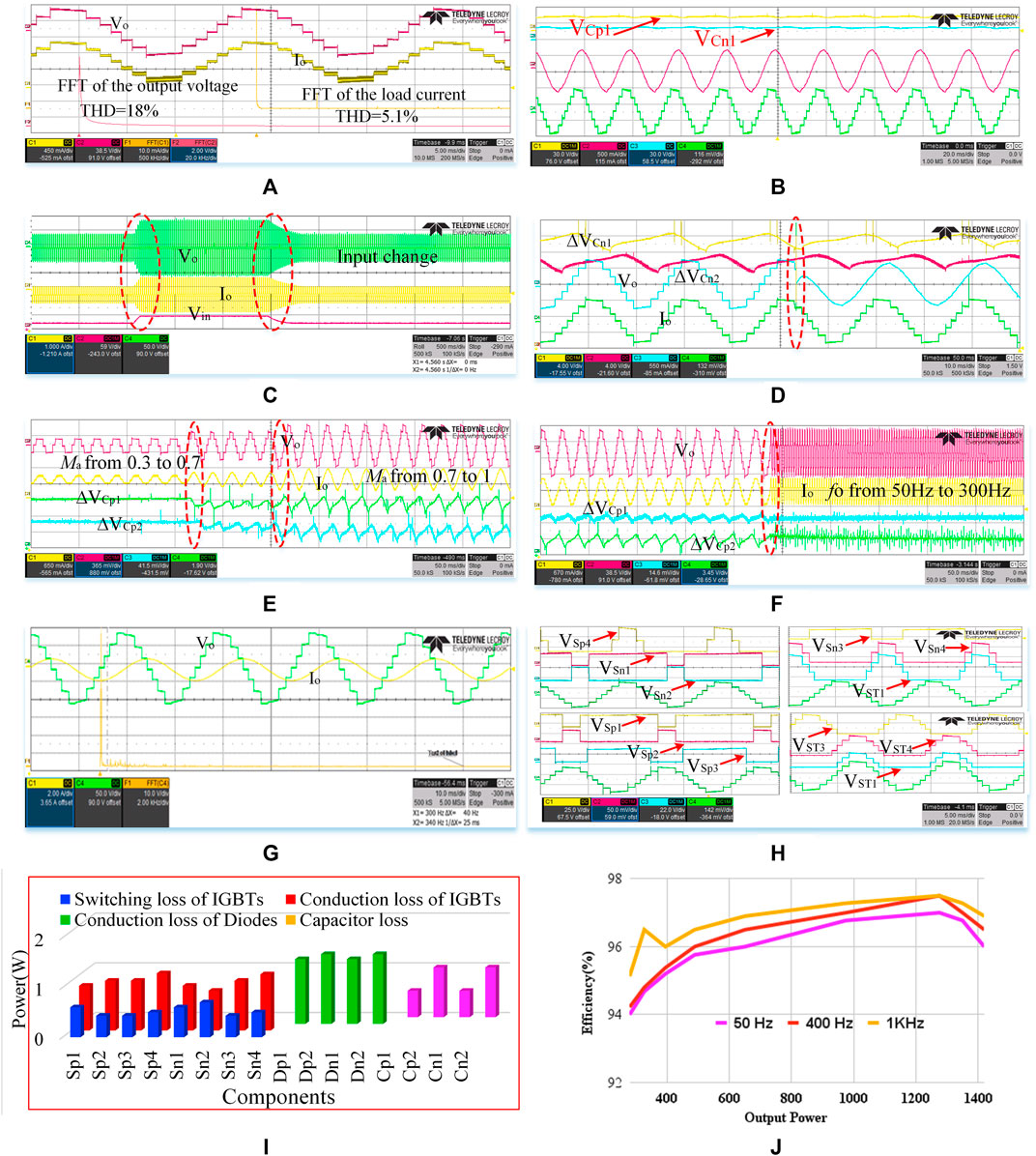
FIGURE 2. Experimental validation and power-loss analysis of the proposed topology.
Similar tests were conducted to investigate the feasibility of the inverter in dynamic modes of operation. It was tested for load, input voltage, modulation index, and output frequency variations. The experimental waveforms under the input voltage and load variations are shown in Figures 2C and D. It is clear from Figure 2C that the operation of the inverter is very stable for transient changes in input voltage from 30 to 60 V and vice versa. The experimental waveforms are shown in Figure 2D to verify the performance of the inverter for a step change in load from an R-load (R = 100 Ω) to an RL-load (R = 100 Ω, L = 100 mH). While the voltage across the capacitors remains balanced during transient variation in load. It can be observed that the peak magnitude of the voltage ripples of Cp1 and Cn1 was about 3.5 V; as for Cp2 and Cn2, they were approximately 4.1 V.
In the end, the inverter was tested with a step change in modulation index (Ma) and output frequency. The results are captured in Figures 2E and F. When Ma was suddenly changed from 0.3 to 0.7 and then to 1, seven, five, and three voltage levels were achieved in the output, respectively, and the load current also increased accordingly. The load current affects the magnitude of discharging current of the SCs, and therefore, it influences the discharge amount of the SCs, which will, in turn, influence the ripples of the capacitor voltage. The results under the condition of a step change of the output frequency (fo) are shown in Figure 2F. It can be observed that the output voltage waveforms were unaffected during either the modulation index or frequency transient. The results confirmed that the proposed inverter was able to adapt to sudden variations in modulation index and load. Figure 2G shows the experimental results at an RL-load (R = 10 Ω, 200 mH) to show the validity of the proposed inverter at low power factors. The blocking voltage experimental waveforms for different switches are captured in Figure 2H. The maximum blocking voltage of the switches in Su1, 1, Su1, 2, Sl1, 1, Sl1, 2, Su2, 1, and Sl2, 1 was within 30 V. The maximum blocking voltage for Su2, 2 and Sl2, 2 was 60 V. The maximum blocking voltage for ST1 and ST2 was within 90 V. In a similar way, the maximum blocking voltage for switches ST3 and ST4 was within 120 V.
The power-loss analysis of the seven-level topology has been carried out in this section. At 158 W measured output power of the inverter, the total loss of the topology observed from the circuit was 16.26 W (input power = 175 W). At this power, the efficiency of 90.28% was reported with a high switching technique (10 kHz). Then, a detailed power-loss analysis was carried out for the proposed seven-level inverter using PLECS simulation software. Here, the inverter efficiency, loss distribution among power components, and temperature profile of switches in steady-state conditions for the proposed SC inverter were analyzed over a wide range of output power.
In the following analysis, the parameters taken into consideration at steady-state conditions are the following: (a) IGBT loss (both switching loss and conduction loss), (b) diode conduction loss, and (c) capacitor equivalent series resistance loss or ripple loss. In this case, the input voltage source was set to 300 V. With the parameters used for experimental testing, the proposed seven-level inverter was modeled and implemented in PLECS. The thermal modeling of the semiconductor devices was developed from the datasheet of the IKY75N120CH3 module manufactured by Infineon Technologies AG. The parasitic resistances of the capacitors (1200 μF) were set at 0.1Ω. The loss distribution among power components in steady-state conditions for the proposed SC inverter is given in Figure 2I.
The measured efficiencies for different operation frequencies with a unity power factor at various power loads such as 0.3, 0.4, 0.5, 0.6, 0.9, 1.2, and 1.4 kW are plotted in Figure 2I. It can be observed that the proposed seven-level SCMLI gave maximum efficiency of 97.5% at 1276 W for 400 Hz and 1 kHz. Overall, the observed effects of the output current and frequency on the conversion efficiency coincided with the theoretical analysis. The ripple losses were not dominating at light load, and the simulated efficiencies at operating frequencies (50 Hz, 400 Hz, and 1 kHz) were very close to each other. The simulated efficiency for the seven-level inverter was about 97.5%. When the output power was gradually increased, the conversion efficiency became significantly improved at 1 kHz over 50 Hz, along with the reduction in the voltage ripples of SCs. By increasing the frequency at 350 Ω load, the efficiency increased from 94 to 96%. However, the efficiency variation measured between 400 Hz and 50 kHz was insignificant because of the large RC-time constant of the SCs selected in the prototype.
In this article, a new SC-based inverter with a low switch count was suggested. Also, the CMV was significantly minimized by connecting the neutral of the output terminal to the midpoint of dc-link capacitors. In addition, SCs were charged beyond half-cycle, which minimized the capacitor’s voltage ripples and current spikes during the SC charging process. Moreover, the proposed structure featured main advantages such as a low number of conducting switches in current flow paths and SC charging paths. Moreover, the current flow among SCs was restricted. This is a benefit because the charging current only flows from the dc-link capacitor to the SCs. The comparative analysis and cost comparison against its benchmarked topology (SC-MTI) and recently introduced SCMLIs confirmed the superiority of the proposed SCMLI. Further, the performance of the proposed inverter was verified by conducting experimental tests at steady- and dynamic-state conditions. The tests were performed at different loadings and modulation indices. The additional feature of the proposed inverter was its capability to integrate inductive loads. In the end, a PLECS power-loss modeling and conversion efficiency evaluation was provided for the proposed topology.
The original contributions presented in the study are included in the article/supplementary material. Further inquiries can be directed to the corresponding authors.
SK contributed to the conception and methodology and performed the analysis. SK wrote the first draft of the manuscript. SK and MA wrote sections of the manuscript. SA and NN supervised this work. SM, MS, and AS arranged the funding acquisition. All authors contributed to the manuscript, read, and approved the submitted version.
The APC for this work is funded through Universiti Tenaga Nasional grant no. IC6-BOLDREFRESH2025 (HCR) under the BOLD2025 Program.
The authors declare that the research was conducted in the absence of any commercial or financial relationships that could be construed as a potential conflict of interest.
The handling editor NP is currently organizing a research topic with the author SM.
All claims expressed in this article are solely those of the authors and do not necessarily represent those of their affiliated organizations, or those of the publisher, the editors, and the reviewers. Any product that may be evaluated in this article, or claim that may be made by its manufacturer, is not guaranteed or endorsed by the publisher.
Ali, J. S. M., and Krishnasamy, V. (2018). Compact switched capacitor multilevel inverter (CSCMLI) with self-voltage balancing and boosting ability. IEEE Trans. Power Electron. 34 (5), 4009–4013. doi:10.1109/tpel.2018.2871378
Barzegarkhoo, R., Lee, S. S., Khan, S. A., Siwakoti, Y. P., and Lu, D. D-C. (2021). A novel generalized common-ground switched-capacitor multilevel inverter suitable for transformerless grid-connected applications. IEEE Trans. Power Electron. 36 (9), 10293–10306. doi:10.1109/tpel.2021.3067347
Chen, M., Yang, Y., Liu, X., Chiang, P., and Blaabjerg, F. (2021). Single-source cascaded multilevel inverter with voltage-boost submodule and continuous input current for photovoltaic applications. IEEE Trans. Power Electron. 37, 955–970. doi:10.1109/tpel.2021.3098015
Das, C. K., Kirubakaran, A., and Somasekhar, V. (2021). A quasi Z-source based five-level PV inverter with leakage current reduction. IEEE Trans. Ind. Appl. 58, 400–412. doi:10.1109/tia.2021.3119526
He, L., Sun, J., Lin, Z., and Cheng, B. (2021). Capacitor-voltage self-balance multilevel inverter with unequal amplitude carrier-based APODPWM. IEEE Trans. Power Electron. 36, 14002. doi:10.1109/TPEL.2021.3089620
Hussan, M. R., Sarwar, A., Siddique, M. D., Iqbal, A., and Alamri, B. (2021). A cross connected asymmetrical switched-capacitor multilevel inverter. IEEE Access 9, 96416–96429. doi:10.1109/ACCESS.2021.3093826
Iqbal, A., Siddique, M. D., Prathap Reddy, B., Maroti, P. K., and Alammari, R. (2020). A new family of step-up hybrid switched-capacitor integrated multilevel inverter topologies with dual input voltage sources. IEEE Access 9, 4398–4410. doi:10.1109/ACCESS.2020.3046192
Iqbal, A., Siddique, M. D., Prathap Reddy, B., and Maroti, P. K. (2021). Quadruple boost multilevel inverter (QB-MLI) topology with reduced switch count. IEEE Trans. Power Electron. 36, 7372–7377. doi:10.1109/TPEL.2020.3044628
Kakar, S., Ayob, S., Arif, M. S. B., Nordin, N., Daud, Z., Ayop, R., et al. (2021a). A new multilevel inverter topology based on switched-capacitor technique. Int. J. Power Electron. Drive Syst. 12 (1), 627. doi:10.11591/ijpeds.v12.i1.pp627-636
Kakar, S., Ayob, S. B. M., Iqbal, A., Nordin, N. M., Arif, M. S. B., Gore, S., et al. (2021b). New asymmetrical modular multilevel inverter topology with reduced number of switches. IEEE Access 9, 27627–27637. doi:10.1109/access.2021.3057554
Khan, M. N. H., Forouzesh, M., Siwakoti, Y. P., Li, L., and Blaabjerg, F. (2020). Switched capacitor integrated (2n+ 1)-level step-up single-phase inverter. IEEE Trans. Power Electron. 35 (8), 8248–8260. doi:10.1109/tpel.2019.2963344
Lee, S. S., Bak, Y., Kim, S-M., Joseph, A., and Lee, K-B. (2019a). New family of boost switched-capacitor 7-level inverters (BSC7LI). IEEE Trans. Power Electron. 34, 10471. doi:10.1109/TPEL.2019.2896606
Lee, S. S., and Lee, K-B. (2019). Dual-T-type seven-level boost active-neutral-point-clamped inverter. IEEE Trans. Power Electron. 34 (7), 6031–6035. doi:10.1109/tpel.2019.2891248
Lee, S. S., and Lee, K-B. (2020). Switched-Capacitor-based modular T-type inverter (SC-MTI). IEEE Trans. Industrial Electron. 68, 5725. doi:10.1109/TIE.2020.2992963
Lee, S. S., Lim, C. S., and Lee, K-B. (2019b). Novel active-neutral-point-clamped inverters with improved voltage-boosting capability. IEEE Trans. Power Electron. 35 (6), 5978–5986. doi:10.1109/tpel.2019.2951382
Lee, S. S., Lim, C. S., Siwakoti, Y. P., and Lee, K-B. (2019c). Hybrid 7-level boost active-neutral-point-clamped (H-7L-BANPC) inverter. IEEE Trans. Circuits Syst. II. 67 (10), 2044–2048. doi:10.1109/tcsii.2019.2946860
Lin, W., Zeng, J., Fu, B., Yan, Z., and Liu, J. (2021). Switched-capacitor based seven-level boost inverter with reduced devices. CSEE J. Power Energy Syst., 1–11. doi:10.17775/CSEEJPES.2020.02620
Mustafa, U., Arif, M. S. B., Kennel, R., and Abdelrahem, M. (2022). Asymmetrical eleven-level inverter topology with reduced power semiconductor switches, total standing voltage and cost factor. IET Power Electron. 15 (5), 395–411. doi:10.1049/pel2.12238
Peng, W., Ni, Q., Qiu, X., and Ye, Y. (2019). Seven-level inverter with self-balanced switched-capacitor and its cascaded extension. IEEE Trans. Power Electron. 34, 11889–11896. doi:10.1109/tpel.2019.2904754
Rech, C. (2019). “Modified five-level anpc inverter with output voltage boosting capability,” in IECON 2019-45th Annual Conference of the IEEE Industrial Electronics Society, Lisbon, Portugal, 14-17 October 2019 (IEEE).
Roy, T., and Sadhu, P. K. (2020). A step-up multilevel inverter topology using novel switched capacitor converters with reduced components. IEEE Trans. Ind. Electron. 68, 236–247. doi:10.1109/tie.2020.2965458
Roy, T., Sadhu, P. K., and Dasgupta, A. (2019). Cross-switched multilevel inverter using novel switched capacitor converters. IEEE Trans. Ind. Electron. 66 (11), 8521–8532. doi:10.1109/tie.2018.2889632
Roy, T., Tesfay, M. W., Nayak, B., and Panigrahi, C. K. (2021). A 7-level switched capacitor multilevel inverter with reduced switches and voltage stresses. IEEE Trans. Circuits Syst. II. 68, 3587–3591. doi:10.1109/tcsii.2021.3078903
Saeedian, M., Adabi, M. E., Hosseini, S. M., Adabi, J., and Pouresmaeil, E. (2019). A novel step-up single source multilevel inverter: Topology, operating principle, and modulation. IEEE Trans. Power Electron. 34 (4), 3269–3282. doi:10.1109/tpel.2018.2848359
Saeedifard, M., Barbosa, P. M., and Steimer, P. K. (2011). Operation and control of a hybrid seven-level converter. IEEE Trans. Power Electron. 27 (2), 652–660. doi:10.1109/tpel.2011.2158114
Sandeep, N., Ali, J. S. M., Verma, A. K., and Yaragatti, U. R. (2020). “Reduced component boost seven-level inverter (RCB7LI) with self-voltage balancing,” in 2020 IEEE International Conference on Power Electronics, Smart Grid and Renewable Energy (PESGRE2020), Cochin, India, 02-04 January 2020 (IEEE).
Sathik, M. J., Almakhles, D. J., Sandeep, N., and Siddique, M. D. (2021). Experimental validation of new self-voltage balanced 9L-ANPC inverter for photovoltaic applications. Sci. Rep. 11, 5067. doi:10.1038/s41598-021-84531-z
Sathik, M. J., Sandeep, N., and Blaabjerg, F. (2019). High gain active neutral point clamped seven-level self-voltage balancing inverter. IEEE Trans. Circuits Syst. II. 67 (11), 2567–2571. doi:10.1109/tcsii.2019.2955318
Siddique, M. D., Reddy, B. P., Meraj, M., and Iqbal, A. (2022). A new high-level boost inverter topology with reduced device count. Circuit Theory &. Apps. doi:10.1002/CTA.3280
Siwakoti, Y. P. (2018). “A new six-switch five-level boost-active neutral point clamped (5L-Boost-ANPC) inverter.” in 2018 IEEE Applied Power Electronics Conference and Exposition (APEC), San Antonio, TX, USA, 04-08 March 2018 (IEEE)
Siwakoti, Y. P., Mahajan, A., Rogers, D. J., and Blaabjerg, F. (2019a). A novel seven-level active neutral-point-clamped converter with reduced active switching devices and DC-link voltage. IEEE Trans. Power Electron. 34 (11), 10492–10508. doi:10.1109/tpel.2019.2897061
Siwakoti, Y. P., Palanisamy, A., Mahajan, A., Liese, S., Long, T., Blaabjerg, F., et al. (2019b). Analysis and design of a novel six-switch five-level active boost neutral point clamped inverter. IEEE Trans. Ind. Electron. 67, 10485–10496. doi:10.1109/tie.2019.2957712
Taghvaie, A., Adabi, J., and Rezanejad, M. (2017). A self-balanced step-up multilevel inverter based on switched-capacitor structure. IEEE Trans. Power Electron. 33 (1), 199–209. doi:10.1109/tpel.2017.2669377
Wang, H., Kou, L., Liu, Y-F., and Sen, P. C. (2017). A new six-switch five-level active neutral point clamped inverter for PV applications. IEEE Trans. Power Electron. 32 (9), 6700–6715. doi:10.1109/tpel.2016.2623568
Xiao, H. (2020). Overview of transformerless photovoltaic grid-connected inverters. IEEE Trans. Power Electron. 36 (1), 533–548. doi:10.1109/tpel.2020.3003721
Ye, Y., Hua, T., Chen, S., and Wang, X. (2021). Neutral-point-clamped five-level inverter with self-balanced switched capacitor. IEEE Trans. Ind. Electron. 69 (3), 2202–2215. doi:10.1109/tie.2021.3066932
Keywords: multilevel inverters, switched capacitor, neutral-point clamped, common-mode voltage, voltage boosting
Citation: Kakar S, Arif MSB, Ayob SM, Nordin NBM, Mekhilef S, Seyedmahmoudian M and Stojcevski A (2022) An improved seven-level switched-capacitor-based neutral-point clamped inverter. Front. Energy Res. 10:957825. doi: 10.3389/fenrg.2022.957825
Received: 31 May 2022; Accepted: 28 June 2022;
Published: 04 August 2022.
Edited by:
Natarajan Prabaharan, SASTRA University, IndiaReviewed by:
Md. Reyaz Hussan, Qatar University, QatarCopyright © 2022 Kakar, Arif, Ayob, Nordin, Mekhilef, Seyedmahmoudian and Stojcevski. This is an open-access article distributed under the terms of the Creative Commons Attribution License (CC BY). The use, distribution or reproduction in other forums is permitted, provided the original author(s) and the copyright owner(s) are credited and that the original publication in this journal is cited, in accordance with accepted academic practice. No use, distribution or reproduction is permitted which does not comply with these terms.
*Correspondence: M. Saad Bin Arif, c2FhZGJpbmFyaWZAZ21haWwuY29t; Shahrin Md. Ayob, c2hhaHJpbkBma2UudXRtLm15
Disclaimer: All claims expressed in this article are solely those of the authors and do not necessarily represent those of their affiliated organizations, or those of the publisher, the editors and the reviewers. Any product that may be evaluated in this article or claim that may be made by its manufacturer is not guaranteed or endorsed by the publisher.
Research integrity at Frontiers
Learn more about the work of our research integrity team to safeguard the quality of each article we publish.