
95% of researchers rate our articles as excellent or good
Learn more about the work of our research integrity team to safeguard the quality of each article we publish.
Find out more
BRIEF RESEARCH REPORT article
Front. Energy Res. , 07 October 2022
Sec. Smart Grids
Volume 10 - 2022 | https://doi.org/10.3389/fenrg.2022.953709
This article is part of the Research Topic Highly Efficient and Reliable Power Converters for Microgrid Applications View all 6 articles
 V. Kubendran1
 Y. Mohamed Shuaib2*
A double capacitor double diode double switch (DCDDDS) multilevel inverter is proposed in this paper to generate positive voltage and connect a polarity changing circuit of H-bridge inverter that generates negative voltage. The desired level is achieved by connecting the jth number of basic units in series. To generate more stepped levels with fewer switches, various algorithms, such as Natural, Binary, Trinary, and Quasi-Linear sequences, and two new proposed algorithms are discussed to determine the magnitude of DC voltage sources. The proposed multilevel inverter eliminates the need to turn on more power switches for different levels, which is the highlight of this topology. The proposed multilevel inverter is compared in terms of the switch count, number of ON state switches per level, driver circuits, and total standing voltage with the conventional switched diode multilevel inverters. Real-time results from the test bench of OPAL-RT and simulation have been used to validate the proposed inverter.
Multilevel Inverters offer several advantages over traditional two-level inverters, such as having less total harmonic distortion because the output voltage and current are almost similar to a sinusoidal wave, high efficiency, reduced switching losses, and less peak inverse voltage depending on properly designed topologies. Initially, (Nabae et al., 1981; Meynard and Foch, 1992; Rodriguez et al., 2009) three MLI topologies, namely Neutral Point Clamped MLI (NPC MLI), Flying Capacitor MLI (FC-MLI) and Cascaded H-Bridge MLI (CHB MLI), were developed in the literature; consequently, the inverter output power is improved and the total harmonic distortion is reduced, however, the number of power switches and clamping diodes will increase when the stepped level increases in NPC MLI. Similarly, increasing the single positive and negative stepped level in CHB MLI requires an additional four switches and one dc source, which is the main issue of this topology. Because of high modularity, many researchers have focused on improving conventional cascaded multilevel inverters based on the number of switches with the driver circuit, maximum blocking voltage of each switch including the total standing voltage of the inverter, the number of sources, power losses, and Total Harmonic Distortion. In (Babaei and Hosseini, 2009), Ebrahim Babaei et al. conferred a semi-bridge type sub-multilevel. The author provides three methods for determining unequal dc magnitudes of sub-multilevel to increase the steps in the output wave without increasing switch count and dc sources. Though this structure has less blocking voltage than others, it needs to turn on more switches to obtain a higher level (Wang et al., 2017). Lei Wang modified the structure proposed by Ebrahim Babaei where one additional switch is connected to remove the spike at the time of reverse current. As the level increases, the number of turn-on switches increases despite providing fewer blocking voltages than other structures and reducing voltage spikes. Ebrahim Babaei et al. developed a basic unit in (Babaei et al., 2014) that generates three positive output staircase levels; to increase the voltage output stepped levels, the basic unit is connected by cascade, thus resulting in a more expensive and bulkier inverter design. In addition, this structure needs auxiliary structures to create first positive stepped levels. In this article, the author explains four different algorithms for choosing DC sources for higher-level generation. Rasoul Shalchi Alishah et al. (Alishah et al., 2014a; Alishah et al., 2014b; Alishah et al., 2014c) have suggested a new switched diode multilevel inverter structure. In this topology, sub cell or sub multilevel consists of a single switch, a single diode, and a single dc source. The number of positive stepped levels depends on the number of cells connected in series. As the number of cells in series increases, the number of activated switches or conducting switches increases linearly, which will cause a significant increase in conduction losses. Consequently, power losses can occur. To generate a negative stepped output voltage level from this topology, H-bridge circuit is needed. Mohammad Ali Hosseinzadeh et al. (2020) developed a switched-diode MLI that consists of three switches, three diodes, and three sources to generate seven levels during equal dc source value. The author has discussed two different methods to select the dc source value for generating high-stepped output level with a lower number of switch count. Although this topology uses fewer power switches and driver circuits, it does not work for a power factor less than 0.99 because, during RL load, the voltage spikes are generated at positive and negative zero levels. This is due to the reverse current. Babak Hosseini Montazer et al. solved this problem in (Hosseini Montazer et al., 2021) through the creation of a new structure for bidirectional current flow. Nevertheless, this requires more switches and driver circuits. Furthermore, the number of conducting power switches increases as the number of levels increases, which results in greater conduction losses. A novel Cascaded H-bridge multilevel inverter is propounded (Seifi et al., 2020) by Ali Seif. The basic structure of this topology is three positive output stepped levels with five switches, three sources, and a single diode. Despite this structure having fewer switches and driver circuits, the total blocking voltage is quite high. Dhafer Almakhles et al. suggested (Sathik et al., 2021a) Symmetrical Diode based Half- Bridge MLI; the basic module this topology produces is a positive stair cases of two levels with two switches, two diodes, two sources, and two dc link capacitors, however a balancing circuit is required, so when two capacitors are connected in series, the voltage across each capacitor is not equal. Voltage divider circuits are used to equalize the capacitor voltage, which will increase the inverter component and size. Trinary sequence algorithms have been discussed as a way to create higher levels with fewer switches and diodes from this topology. Kaibalya Prasad Panda et al. (Panda and Panda, 2018; Panda et al., 2020) discussed double-source switched diode with unequal DC sources to generate a positive stair-level output. This circuit requires fewer driver circuits with fewer switches, but the source requirements for this structure increases as the level increases, i.e. the main issue with this structure is that it requires four dc sources to produce three positive levels. A novel Switched Diode Multilevel Inverter with fewer switches was created by Ahamed Ibrahim et al. (Panda et al., 2019). The blocking voltage and ON state switches are the topology’s advantages, but the problem with it is that every single basic unit needs one bidirectional switch. Kaibalya Prasad Panda (Hosseinpour et al., 2020) created a switched-diode dual source single switch based multilevel inverter. The problem with this design is that when the number of levels is increased, more switches need to be turned on. The bidirectional diode-based multilevel inverter topology with decreased switch was created by Hosseinpour et al. (Ahamed Ibrahim et al., 2019). Although this architecture has fewer switches overall, it has more bidirectional switches, which is its greatest issue. The T-Type inverter is a modified design by Bidyut Mahato et al. (Mahato et al., 2021). Upward sequential cells produce positive levels, and downward sequential cells produce negative levels. There are no bidirectional switches required, and there is less total standing voltage, but when the level increases, the number of cells (single dc source, switch, and diode) required increases as well. The same number of cells should be connected on both sides of the inverter so that an equal level is produced on each half-cycle. The main weakness of this converter is that the number of cells increases on both sides as the number of levels increases. This leads to increased number of turn on switches. According to the literature survey, to increase the level of a switched-diode multilevel inverter, more switches will need to be active; this will increase the conduction losses and energy losses. Conduction losses can be reduced by reducing the conduction duration of the switches. The proposed DCDDDS topology uses fewer on-state switches to produce more levels.
The following are the most important aspects of this work:
• More levels can be achieved with fewer switches in generalized Double dc link capacitor Double Diode Double Switch-based multilevel inverters.
• In relation to the level, the quantity of on-state switches is minimized.
• The proposed multilevel inverter with fewer ON-sate switches can handle both symmetrical and asymmetrical sources. During unequal dc source selection, two algorithms are proposed: proposed algorithm 1 and proposed algorithm 2 (Combination of trinary and quadruple sequences).
• This paper provides the number of levels pertaining to the fundamental units that can generate the desired level using an appropriate algorithm. It is necessary to know the cumulative standing voltage of the topology as well as the blocking voltage at each switch to select the best algorithm.
• Modified multicarrier PWM modulation for reducing THD and improving voltage RMS values is described.
The basic unit of Double dc link capacitor (C1, C2) Double Diode Double Switch (DCDDDS)-based multilevel inverter are designed to generate a positive sequence of two levels, shown in Figure 1A, and the auxiliary unit consists of one switch and two switches, which is illustrated in Figure 1B. Figure 1C shows the typical waveform of output voltage. The first positive level of VC2 is generated when switch S2 is turned on; similarly, the second positive level of VC2 + VC1 is generated when switch S1 is turned ON. The switching pattern for the basic unit is depicted in Figure 1D. The switch S1 blocks the voltage of VC2 + VC1 and switch S2 blocks the voltage of VC2. With the help of polarity-changing circuit, the negative cycle of VC2 and VC2 + VC1 are generated. The main issue with the polarity-changing circuit is that each switch blocks the voltage of Vo. In Figure 1A, the Vo represents the maximum voltage across the terminal and the number of levels can be increased by connecting the basic units in series. Figure 1E shows the generalized structure of basic units with an auxiliary circuit used in symmetrical and asymmetrical multilevel inverters. In this, a dc-link capacitor is balanced using a balancing circuit of Multilevel-Boost Converter. Each unit generates output voltages V01, V02, V03 … V0j respectively. The output voltage of the first unit is computed as VC2 + VC1, similarly for all basic units. Accordingly, the proposed generalized configuration requires the following number of components.
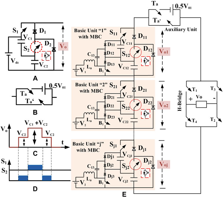
FIGURE 1. (A) Basic unit of proposed Multilevel Inverter. (B) Auxiliary unit. (C) Voltage across the terminal. (D) switching pulse for proposed unit. (E) Generalized Proposed DCDDDS Multilevel Inverter Structure.
In this configuration, “j” is the number of basic units that are connected in series. The proposed DCDDDS multilevel inverter can handle both equal and unequal magnitude dc sources. The selection of a dc source during unequal magnitude is described in section 2.2.
The voltage across each dc-link capacitor in all of the basic units is the same, because the dc-link capacitors are balanced by a balancing circuit. As a result, the voltage across the terminal of each basic unit is equal to the sum of the voltages across its dc-link capacitors Voj = VCj1 + VCj2. Taking the jth unit as an example, the Total Standing Voltage is 11j+4 and the number of levels is 4j+3. In this method, the auxiliary unit switches Ta and Ta’ are redundant so V1 is directly connected to the basic unit 1. The auxiliary dc source magnitude is considered to be half of Vo1.
There are two ways to raise the stepped level: First, extend the basic unit into a series arrangement. This will increase the number of switches, drivers, and DC sources. Second, when the right voltage magnitude is determined by a different algorithm, which is known as an asymmetrical multilevel inverter, the number of levels is increased with fewer units which will reduce the switch count, sources, and driver circuits. Several methods are available to detect dc sources such as natural sequence, quasi linear, binary, trinary, and proposed algorithm 1 and 2. The generalized expression for the above selected sequence of numbers of level and TSV with respect to the number of units are discussed below. It is assumed that the dc source value for the auxiliary unit is voltage across VC11 or 0.5 Vo1 throughout the sequence.
As the input DC voltages increase, the algorithm progresses from 1Vdc to 2Vdc, 3Vdc, 4Vdc... jVdc. According to Eq. 10, the dc-link capacitor voltage must be maintained. Eq. 11 can be used to calculate the algorithm’s stepped output level. Because the magnitude of the dc-link capacitor varies by basic unit, the IGBT rating is determined by the maximum blocking voltage of each switch in each unit. The total standing voltage is calculated by adding all of the switch blocking voltages in the generalized topology.
The Total Standing Voltage of Natural Sequence is
A binary method is used to determine the magnitudes of dc voltage sources, which results in an exponential increase in the levels of the overall outputs with dc voltages. With the binary algorithm the value of dc source is VCj1 = VCj2 = 2i Vdc, i = j-1, j = 1, 2, 3….. Hence, the general expression for the number of levels is 2(j+2) -1. The switch Sj1 blocks the voltage of VCj1 plus VCj2; similarly, the switch Sj2 blocks the voltage of VCj2. The total standing voltage of the binary algorithm is expressed as
The dc source value in the trinary sequence is calculated using the power of three, which is VCj1 = VCj2 = 3i Vdc. This can generate levels of 2 (3i) +1. The expression of total standing voltage for this algorithm is given below.
The voltage magnitude of each basic unit is determined by Eq. 15. The number of levels generated from this algorithm is 4 (3j−1+3). Based on Eq. 16, the TSV is determined for Quasi-Linear algorithm.
According to Eq. 17 above, the dc source value for the first unit is Vdc, while the remaining units have a voltage of 4Vdc to generate 2 (8i) +7 number of levels. In a similar fashion, the total standing voltage for jth unit of proposed algorithm is
The generalized structures shown in Figure 1E are divided into odd and even numbers of units using this algorithm. The trinary sequence, which means power of three, determines the odd unit dc source values, while the quadruple sequence, which means power of four, determines the even unit dc source values, as shown in Eq. 18. The total standing voltage and number of stepped levels are investigated using Eqs 19, 20.
In terms of component count factor, cost function, number of stepped levels, diode requirement, and total standing voltage, the proposed DCDDDS switched diode multilevel inverter is compared with conventional topologies of the switched diode.
The primary goal of researchers today is to reduce the component count factor of the inverter. In general, higher factor values indicate a need for more components at a given output voltage level. The reduction of factor values has thus become increasingly important in multilevel inverter topologies. From graph 2. D, the similar topology (switched-diode) presented in R2, R7, and R8 (Proposed DCDDDS MLI) has the same number of component counts per level. Though the presented topology in R3 has lower component counts per level than the proposed topology, but turn on switch count with respect to level little more which is tabulated in Table 1. The Proposed DCDDDS MLI has a lower component count when compared to conventional topologies (R1, R5, R6, and R4).

TABLE 1. Comparison of different Switched-Diodes with Proposed DSDDDS.
In order to calculate the total cost of the multilevel inverter, a cost function (CF) is used to calculate all the components of the inverter module, including power semiconductor switches (Nsw), capacitors (NC), driver circuit (NDRI), number of Sources (NDCS), number of Diode (NDI) and weight coefficient multiplied with per unit of Total standing Voltage. Eq. 22 (Prasad et al., 2021) represents the formula used to calculate the cost factor. In the equation, “α” represents the weight coefficient, and the value is chosen to be greater or lower than one. The cost function of DCDDDS and conventional switched-diode structures are given in Table 1.
Table 1 shows the proposed DCDDDS structure with a similar switched diode conventional structure and provides the switch count, the number of drivers required, and the blocking voltage of the topology. The dc sources in all basic units from proposed DCDDDS inverter are assumed to be symmetrical. Figure 2A clearly shows that the DCDDDS structure requires less total standing voltage than any other switched-diode structure, except R2. Despite the lower standing voltage of the R2 structure, the turn-on switches are proportional to the stepped level, so the conduction losses will increase. In Figure 2C, there is a comparison between number of stepped levels and switch count. The topology presented in R1 and R5 needed more switches. Similarly, the topology presented in R2, R3, R4, R6, and R7 is close to the proposed DCDDDS structure. This clearly shows that the proposed structure requires fewer switches than the other switched-diode MLI structure. Figure 2B depicts the number of diodes used in both the conventional and DCDDDS proposed structures. Therefore, an equal number of diodes must be used to develop the topology presented in R2, R4, R7, and the proposed DCDDDS structure. However, the required number of diodes is lower for R3 and R5, which has a greater need for switches and gate drivers.
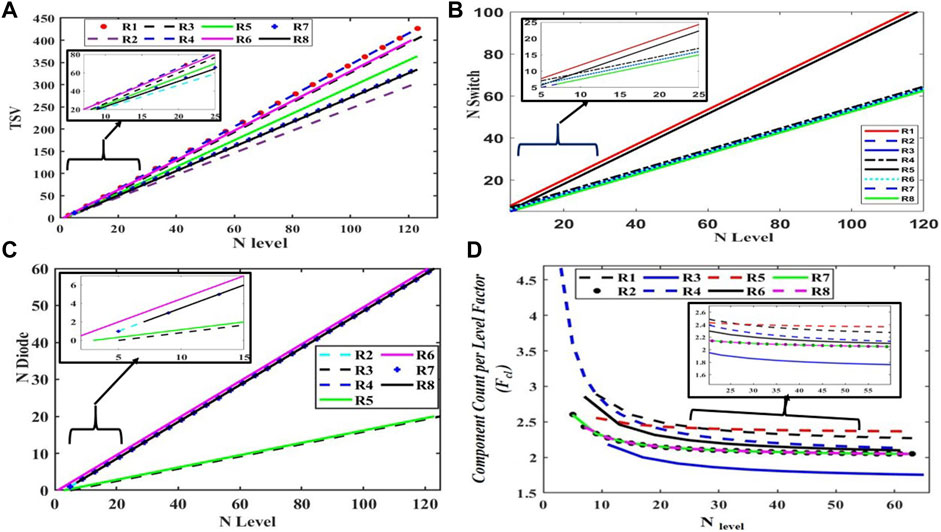
FIGURE 2. Number of stepped level Vs. (A) Total Standing Voltage. (B) Number of Diode. (C) Number of Switches. (D) Component count per level factor.
Figure 3A compares the same configuration of a conventional structure with proposed DCDDDS MLI in order to identify the number of switches that need to be turned on to generate the same level; it considers the symmetrical value of dc source for a conventional as well as proposed MLI. Two and three switches, respectively, are required to be turned on to generate positive stepped first level and second level presented in R2, R3, R5, R7 and proposed DCDDS MLI, whereas conventional structures presented in R1, R4 and R6 require slightly more switches to be turned on to generate the same levels. Generating stepped third, fourth, fifth, and sixth level from DCDDDS MLI needs fewer switches to turn on compared to a conventional structure. As a result, by decreasing the number of on state switches with respect to levels, conduction losses can be minimized and efficiency can be improved by reducing the conduction losses.
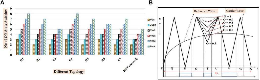
FIGURE 3. (A) The number of turn-on switches for various topologies. (B) Modified Carrier Signal.
Both their conduction and switching transitions are responsible for these losses. Switching losses are the costs associated with turning switches ON and OFF, or transitioning between switches. Conduction losses, on the other hand, result from the switches’ conduction. The power loss analysis should be taken into account while calculating these losses. As a result, various losses have been collected and PLECS software has been used to estimate the proposed converter’s thermal performance. Figure 5 depicts the heat loss profile for the Infineon IKW30N60DTP. Figures 2A–C, respectively, illustrate the thermal description of the turn-on loss, turn-off loss, and conduction loss. With the aid of a heat sink and thermal resistance of 0.75 K/W at an ambient temperature of 25°C, this is obtained in a PLECS environment. The switching losses and conduction losses are illustrated in Figure 4 and the efficiency of the proposed inverter is 97.55%.
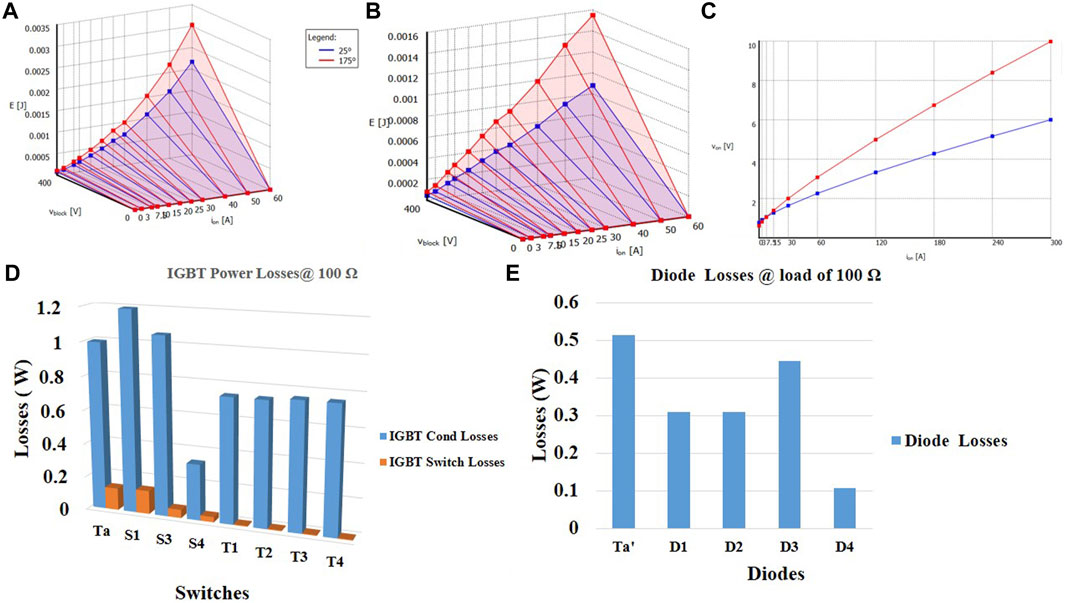
FIGURE 4. Thermal description of IKW30N60DTP (A) ton losses. (B) toff losses. (C) Conduction losses. (D) IGBT power losses calculated using PLECS software. (E) Calculated Diode losses.
In conventional carrier waveforms, the amplitude of the voltage varies from 0 to 1 in the time interval of Ts/2 and from 1 to 0 in the time interval of Ts, respectively, under level-shifted multilevel pulse width modulation. The author of (Sathik et al., 2021b) has modified the traditional carrier wave to improve power quality, i.e., to reduce total harmonic distortion and to increase RMS voltage. Additionally, the modified carrier wave is once again modified in order to reduce the total harmonic distortion. A novel switching scheme based on Level-Shifted multilevel pulse width modulation, under which the carrier wave amplitude is decided by dividing the sampling time period of Ts equally into nine intervals marked in Figure 3B, is proposed to reduce THD. The nine intervals (P-X) are 0 to Ts/8, Ts/8 to 2Ts/8, 2Ts/8 to 3Ts/8, 3Ts/8 to 4Ts/8, 4Ts/8 to 5Ts/8, 5Ts/8 to 6Ts/8, 6Ts/8 to 7Ts/8, and 7Ts/8 to Ts. The amplitude for the corresponding point of carrier wave form changes from 0 to 1, 1 to 0, 0 to 1, 1 to 0.5, 0.5 to 1, 1 to 0, 0 to 1, and 1 to 0 respectively. The proposed pulse width modulation becomes a conventional triangular carrier waveform when the point T amplitude is 0. Similarly, when the amplitude of T is 1, the point between R to V changes to trapezoidal to generate two pulses.
In order to examine whether the proposed MLI is capable of generating a desired stepped output voltage waveform according to the proposed algorithm and conventional algorithm, it has been simulated using MATLAB/SIMULINK. As shown in Figure 1E, two basic circuits with auxiliary circuits are used to analyze the performance of the suggested inverter. In this, the self-balancing circuit of a multilevel boost converter is interfaced between an unregulated source/regulated source and a multilevel inverter circuit in order to balance a dc link capacitor. In a multilevel boost converter, when the source is photovoltaic, the dc-link capacitor voltage is balanced by varying the duty cycle of switches B1 and B2. Initially, the proposed inverter is validated using the trinary sequence algorithm. From a trinary sequence, the voltage magnitudes of the first basic units (V11) are assumed to be 10 V, and the voltage magnitudes of the second basic unit are assumed to be three times the magnitude of the first basic unit. The voltage magnitude of the auxiliary unit is equal to the voltage across the dc-link capacitor of C11. Figure 5A, illustrates the load voltage and current for a trinary sequence and Figure 5B proves that the dc-link capacitor voltage is balanced with the help of a multilevel boost converter. The proposed DCDDDS multilevel inverter with trinary sequence is examined with modulation indices of 1, 0.6, 0.4, and 0.2. As modulation indices decrease, the number of levels decreases. According to the modulation index, 19 levels are created if it is in unity, while thirteen, nine level, and five level are created if it is 0.6, 0.4, and 0.2, respectively. Even after varying modulation indices, the dc-link capacitor voltage remains balanced. Furthermore, the two proposed algorithms are evaluated on the same circuit depicted in Figure 1E. The auxiliary unit and first basic unit values remain the same. The second basic unit’s dc source value is four times that of the first unit. Figure 5C shows the results of using dynamic load changes to study load voltages and currents.
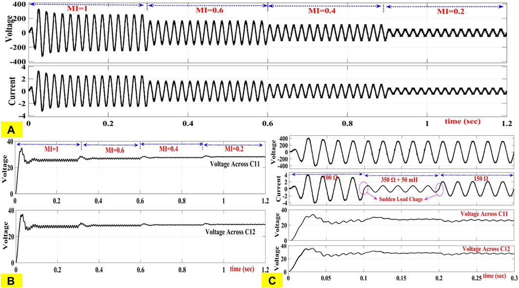
FIGURE 5. (A) Load Voltage and Current Waveforms for Various Modulation Indices in a Trinary Sequence. (B) Balanced Capacitor for Various Modulation Indices in a Trinary Sequence. (C) Load voltage and current wave form during dynamic load changes.
To obtain test results, a test bench called the OPAL-RT is used. RT-LAB is used to build Simulink models, which are loaded to the OPAL-RT 4510 real-time interface. A digital storage oscilloscope records real-time analog voltage and current outputs of the proposed DCDDDS MLI. OPAL-RT 4510 can output 15V to -15V as its maximum output voltage. Figure 6A depicts the experimental setup of the proposed DCDDDS MLI for real-time simulations of OPAL-RT. The resistive load of 100 Ω is connected to the proposed topology for analysis trinary and proposed sequence-based dc source. First, the trinary sequence has been tested by setting the dc sources Vj1 and Vj2 to 10 and 30V, respectively, and the auxiliary source’s value is half that of Vo1. In order for the real-time tech bench to give accurate results, the load voltage and balanced dc-link capacitor voltage must be lowered and kept between +15 and -15. The test result of the proposed DCDDDS with the ratio of 1:3 (trinary sequence) load voltage, load current, and balanced dc-link capacitor voltage from a real-time test bench is depicted in Figure 6B. The dc source values of basic units 1 and 2 are the same for the proposed algorithm 1 and 2, but the dc source values differ from the third to the jth unit basic unit. The proposed topology with the proposed algorithm 2 sequence was tested with various loads, and Figure 6C shows the variation in load voltage and current under dynamic load changes. In the first second, the resistive load of 100 Ω is connected, in the next second the RL load of 350Ω + 50 mH is connected, and in the last second the resistive load of 150 Ω is connected for the validation of inverter performance.
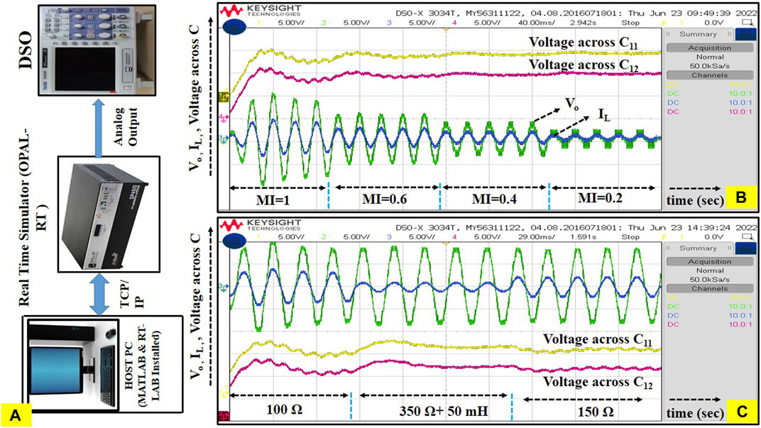
FIGURE 6. (A) real time test bench. (B) Different modulation indices under trinary sequence algorithm. (C) Dynamic load changes during proposed algorithm 2.
The generalized Double Source Double Diode Double Switch with reduced switch count multilevel inverter has been presented and it has been verified that fewer switches are needed to turn on to generate the desired level for symmetrical and asymmetrical values of dc source. The proposed multilevel inverter was verified against different algorithms for generating desired levels and for the same algorithm total standing voltage is also calculated. Compared with symmetric, natural, binary, natural sequence, and quasi-linear algorithms described in the literature, the proposed algorithms deliver a larger number of output levels with lower switch count for lesser basic units. The trinary and proposed algorithm has been tested and the results are verified using simulation and a real-time test bench.
The original contributions presented in the study are included in the article/supplementary material, further inquiries can be directed to the corresponding author.
VK: Conceptualization, original draft, and Writing, VK and YS: examined the simulation and obtained real-time simulator results.
The authors declare that the research was conducted in the absence of any commercial or financial relationships that could be construed as a potential conflict of interest.
All claims expressed in this article are solely those of the authors and do not necessarily represent those of their affiliated organizations, or those of the publisher, the editors and the reviewers. Any product that may be evaluated in this article, or claim that may be made by its manufacturer, is not guaranteed or endorsed by the publisher.
Ahamed Ibrahim, S. A., Anbalagan, P., and Jagabar Sathik, M. A. (2019). A new asymmetric and cascaded switched diode multilevel inverter topology for reduced switches, DC source and blocked voltage on switches. J. Circuits, Syst. Comput. 28 (04), 1950064. doi:10.1142/s0218126619500646
Alishah, R. S., Nazarpour, D., Hosseini, S. H., and Sabahi, M. (2014). New hybrid structure for multilevel inverter with fewer number of components for high-voltage levels. IET power Electron. 7 (1), 96–104. doi:10.1049/iet-pel.2013.0156
Alishah, R. S., Nazarpour, D., Hosseini, S. H., and Sabahi, M. (2014). Novel topologies for symmetric, asymmetric, and cascade switched-diode multilevel converter with minimum number of power electronic components. IEEE Trans. Ind. Electron. 61 (10), 5300–5310. doi:10.1109/tie.2013.2297300
Alishah, R. S., Nazarpour, D., Hosseini, S. H., and Sabahi, M. (2014). Switched-diode structure for multilevel converter with reduced number of power electronic devices. IET Power Electron. 7 (3), 648–656. doi:10.1049/iet-pel.2013.0208
Babaei, E., and Hosseini, S. H. (2009). New cascaded multilevel inverter topology with minimum number of switches. Energy Convers. Manag. 50 (11), 2761–2767. doi:10.1016/j.enconman.2009.06.032
Babaei, E., Laali, S., and Bayat, Z. (2014). A single-phase cascaded multilevel inverter based on a new basic unit with reduced number of power switches. IEEE Trans. Ind. Electron. 62 (2), 922–929. doi:10.1109/tie.2014.2336601
Hosseini Montazer, B., Olamaei, J., Hosseinpour, M., and Mozafari, B. (2021). A generalized diode containing bidirectional topology for multilevel inverter with reduced switches and power loss. Int. J. Circ. Theor. Appl. 49 (9), 2959–2978. doi:10.1002/cta.3077
Hosseinpour, M., Seifi, A., and Rahimian, M. M. (2020). A bidirectional diode containing multilevel inverter topology with reduced switch count and driver. Int. J. Circ. Theor. Appl. 48 (10), 1766–1785. doi:10.1002/cta.2810
Hosseinzadeh, M. A., Sarebanzadeh, M., Rivera, M., Babaei, E., and Wheeler, P. (2020). A reduced single-phase switched-diode cascaded multilevel inverter. IEEE J. Emerg. Sel. Top. Power Electron. 9 (3), 3556–3569. doi:10.1109/jestpe.2020.3010793
Karasani, R. R., Borghate, V. B., Meshram, P. M., and Suryawanshi, H. M. (2016). A modified switched-diode topology for cascaded multilevel inverters. J. Power Electron. 16 (5), 1706–1715. doi:10.6113/jpe.2016.16.5.1706
Mahato, B., Majumdar, S., Jana, K. C., Thakura, P., and Kumar Mohanta, D. (2021). Experimental verification of a new scheme of MLI based on modified T-type inverter and switched-diode cell with lower number of circuit devices. Electr. Power Components Syst. 48 (16-17), 1–18. doi:10.1080/15325008.2021.1906793
Meynard, T. A., and Foch, H. (1992). “Multi-level conversion: High voltage choppers and voltage-source inverters,” in PESC'92 Record. 23rd Annual IEEE Power Electronics Specialists Conference, Toledo, Spain, 29 June 1992 - 03 July 1992, 397–403.
Nabae, A., Takahashi, I., and Akagi, H. (1981). A new neutral-point-clamped PWM inverter. IEEE Trans. Ind. Appl. 1981(5), 518–523. doi:10.1109/tia.1981.4503992
Panda, K. P., Bana, P. R., and Panda, G. (2020). FPA optimized selective harmonic elimination in symmetric–asymmetric reduced switch cascaded multilevel inverter. IEEE Trans. Ind. Appl. 56 (3), 2862–2870. doi:10.1109/tia.2020.2981601
Panda, K. P., Lee, S. S., and Panda, G. (2019). Reduced switch cascaded multilevel inverter with new selective harmonic elimination control for standalone renewable energy system. IEEE Trans. Ind. Appl. 55 (6), 7561–7574. doi:10.1109/tia.2019.2904923
Panda, K. P., and Panda, G. (2018). Application of swarm optimisation-based modified algorithm for selective harmonic elimination in reduced switch count multilevel inverter. IET Power Electron. 11 (8), 1472–1482. doi:10.1049/iet-pel.2017.0697
Prasad, D., Dhanamjayulu, C., Padmanaban, S., Holm-Nielsen, J. B., Blaabjerg, F., and Khasim, S. R. (2021). Design and implementation of 31-level asymmetrical inverter with reduced components. IEEE Access 9, 22788–22803. doi:10.1109/access.2021.3055368
Rodriguez, J., Franquelo, L. G., Kouro, S., Leon, J. I., Portillo, R. C., Prats, M. A. M., et al. (2009). Multilevel converters: An enabling technology for high-power applications. Proc. IEEE 97 (11), 1786–1817. doi:10.1109/jproc.2009.2030235
Sathik, J., Aleem, S. H., Shalchi Alishah, R., Almakhles, D., Bertilsson, K., Bhaskar, M. S., et al. (2021). A multilevel inverter topology using diode half-bridge circuit with reduced power component. Energies 14 (21), 7249. doi:10.3390/en14217249
Sathik, M. J., Almakhles, D. J., Sandeep, N., and Siddique, M. D. (2021). Experimental validation of new self-voltage balanced 9L-ANPC inverter for photovoltaic applications. Sci. Rep. 11 (1), 1–14. doi:10.1038/s41598-021-84531-z
Sedaghati, F., and Majareh, S. H. L. (2019). A multilevel inverter based on cascade connection of submultilevel units with reduced switch count. Int. J. Circ. Theor. Appl. 47 (7), 1152–1172. doi:10.1002/cta.2638
Seifi, A., Hosseinpour, M., Dejamkhooy, A., and Sedaghati, F. (2020). Novel reduced switch-count structure for symmetric/asymmetric cascaded multilevel inverter. Arab. J. Sci. Eng. 45 (8), 6687–6700. doi:10.1007/s13369-020-04659-4
Keywords: multilevel inverter, DC source selection, ON state switch, pulse width modulation, OPAL-RT
Citation: Kubendran V and Shuaib YM (2022) An improved switched diode multilevel inverter topology with fewer on state switches. Front. Energy Res. 10:953709. doi: 10.3389/fenrg.2022.953709
Received: 26 May 2022; Accepted: 25 July 2022;
Published: 07 October 2022.
Edited by:
Jagabar Sathik, Prince Sultan University, Saudi ArabiaReviewed by:
Adil Sarwar, Aligarh Muslim University, IndiaCopyright © 2022 Kubendran and Shuaib. This is an open-access article distributed under the terms of the Creative Commons Attribution License (CC BY). The use, distribution or reproduction in other forums is permitted, provided the original author(s) and the copyright owner(s) are credited and that the original publication in this journal is cited, in accordance with accepted academic practice. No use, distribution or reproduction is permitted which does not comply with these terms.
*Correspondence: Y. Mohamed Shuaib, bWRzaHVhaWJ5QGNyZXNlbnQuZWR1Y2F0aW9u
Disclaimer: All claims expressed in this article are solely those of the authors and do not necessarily represent those of their affiliated organizations, or those of the publisher, the editors and the reviewers. Any product that may be evaluated in this article or claim that may be made by its manufacturer is not guaranteed or endorsed by the publisher.
Research integrity at Frontiers
Learn more about the work of our research integrity team to safeguard the quality of each article we publish.