 Xiangjian Meng
 Jingyang Fang
95% of researchers rate our articles as excellent or good
Learn more about the work of our research integrity team to safeguard the quality of each article we publish.
Find out more
ORIGINAL RESEARCH article
Front. Energy Res. , 23 August 2022
Sec. Solar Energy
Volume 10 - 2022 | https://doi.org/10.3389/fenrg.2022.929676
This article is part of the Research Topic Smart Solar Photovoltaic Inverters with Grid-Supportive Services View all 9 articles
Distributed static compensators (DSTATCOMs), composed of power converters and passive filters, have been extensively utilized in distribution systems to improve their power quality. For the selection of passive filters, LCL filters with smaller sizes and lower costs are increasingly being adopted to replace the conventional L filters. However, the filter components of LCL filters are normally designed for the application of grid-connected inverters, and therefore, these passive components can be further optimized when applied to the DSTATCOM, where the grid-injected current is mainly capacitive. In this study, the novel LCL-filtered half-bridge DSTATCOM topology is proposed, where the conventional filter capacitor of the LCL filter is replaced by the DC-link capacitors with relatively larger capacitances. As a consequence, the grid-side inductance can be dramatically reduced from the order of millihenry to several microhenries. Furthermore, the current stress of semiconductor switches can be decreased. In addition, the power flow analysis and filter design procedure are presented in this study. It is revealed that a constant DC-link voltage can always be maintained, and the voltage variation across each capacitor can be well regulated with properly designed filters and controllers. Experiments were carried out on a down-scaled laboratory prototype, and simulation and experimental results are presented to verify the effectiveness of the proposed DSTATCOM topology.
Reactive power compensation has been one of the major solutions to resolve power quality (PQ)-related issues caused by the large-scale deployment of induction motors, arc furnaces, and other inductive loads in the distribution system [1]. Traditionally, the static VAR compensator (SVC), such as the thyristor-switched capacitor (TSC) and thyristor-controlled reactance (TCR), served as a simple and straightforward measure for reducing the reactive currents flowing through the transmission lines and regulating the voltages at the point of common coupling. Although being extensively utilized, these reactive power compensators have relatively slow dynamic responses, inflexible reactive power compensation, and may introduce resonances when interacting with the system impedance [1].
Ever since the appearance of the distributed static compensator (DSTATCOM), it has been one of the research focuses in modern power systems and has received increasing attention worldwide due to its advantages such as flexible reactive power compensation, multifunctionality, and elimination of resonances (Dugan et al., 2004). Although different in details, the topologies of DSTATCOM are basically similar structures composed of two parts, namely, power converters and passive filters. It should be noted that transformers can also be involved in the DSTATCOM configuration and considered a part of passive filters (Singh et al., 2014). Passive filters are essential for attenuating high-frequency harmonics introduced by the modulation of power converters. For selection of passive filters, single inductor L filters, which are normally utilized at the medium or high voltage level for applications of the STATCOM and modular multilevel cascade converter (MMCC) (Peng et al., 1996; Liang and Nwankpa, 1999; Akagi, 2011), have been gradually replaced by third-order LCL filters, whose sizes and costs are much reduced, at the low voltage level (Liserre et al., 2005; Kumar and Mishra, 2014a; Fang et al., 2017a).
For DSTATCOM applications, the grid-injected current is mainly capacitive. This characteristic has been widely utilized to optimize the DSTATCOM system to improve its efficiency, compensation ability, and the reduction of system rating (Inzunza and Akagi, 2005; Karanki et al., 2012; Wang et al., 2015). In Inzunza and Akagi (2005), an extra capacitor connected in series with the conventional filter inductor that served as a series LC passive filter has been utilized in the active power filter (APF) application. This extra capacitor exhibits high impedance at the fundamental frequency so that much of the grid voltage appears across this capacitor, resulting in lower output voltage and power rating of the power converter. However, the reactive power compensation ability of this system remains fixed, which is limited by the filter parameters of passive components (Wang et al., 2015). When the same series LC passive filter is applied to the DSTATCOM, the reactive power required by the load can be partly compensated by the filter capacitor while the remaining reactive power is still supplied by the power converter, and therefore, the DC-link voltage of the DSTATCOM can be reduced (Karanki et al., 2012). However, a prominent disadvantage of this series LC topology is the inevitable series resonance, leading to zero impedance at the resonant frequency. Therefore, care must be taken to ensure a zero-converter output voltage near the resonant frequency; otherwise, the output current would become very large. Moreover, the capacitive impedance of this passive filter below the resonance frequency challenges the controller design (Wang et al., 2015). It should be noted that this extra capacitor can also be connected in series with the LCL filter. However, multiple resonances further complicate the aforementioned problems (Kumar and Mishra, 2014a). In Wang et al. (2016a), this series capacitor is replaced by a thyristor-controlled LC reactance, achieving a wide compensation range and low DC-link voltage simultaneously, however, at the expense of increased passive components and system complexity.
In contrast, a filter capacitor shunted with the DSTATCOM can be used to reduce the current stress of semiconductor switches of power converters. In previous references, the shunt capacitor together with the DSTATCOM essentially forms a hybrid filter, and therefore, the design of the whole system becomes much more complicated (Solanki et al., 2015). For another interesting topology proposed in Kumar and Mishra (2014b), an extra inductor is inserted between the shunt capacitor and the power grid. By regulating the voltage across the shunt capacitor, the grid-injected current can be indirectly controlled, and in this case, the DSTATCOM system is actually operated in the voltage control mode. In this case, the shunt capacitor, conventional interfacing inductor, and additional inductor essentially form an LCL filter (Kumar and Mishra, 2015). Indeed, the well-known LCL filter inherently contains a shunt capacitor, which has not been fully utilized for DSTATCOM applications. For all the aforementioned topologies, the filter capacitors of the LCL filters are always designed based on the application of grid-connected inverters (GCIs) (Liserre et al., 2005). As a consequence, the range of capacitances is typically from several to tens of microfarads for limiting the converter reactive current. However, it should be noted that the converter current and, thus, the current stress of semiconductor switches can be decreased with larger filter capacitances of LCL filters in DSTATCOM applications because the capacitor branch loop can bypass much more grid-injected current. Another prominent advantage of using larger filter capacitances is the reduced filter inductance when the resonant frequency of the LCL filter is fixed (Fang et al., 2017a). Furthermore, if the filter capacitor could also serve as the DC-link capacitor, the filter components could be further reduced.
The single-phase pulse-width-modulated (PWM) converters have inherent second-order voltage harmonics in the DC link introduced by the unbalanced instantaneous power between their input and output (Tang et al., 2015a), (Shimizu et al., 1997). These AC voltage components in the DC link distort the compensation current reference and therefore deteriorate the system performance (Tang et al., 2015b; Farivar et al., 2015; Tang and Blaabjerg, 2015). This issue can be solved by either installing large capacitors in the DC link or utilizing active power decoupling strategies (Shimizu et al., 1997; Tang et al., 2015a; Tang et al., 2015b; Farivar et al., 2015; Tang and Blaabjerg, 2015). With the former solution, the voltage fluctuations in the DC link can be decreased. In contrast, the DC-link voltage can be maintained as a constant value using active power decoupling strategies (Tang et al., 2015a), (Shimizu et al., 1997), (Tang et al., 2015b), and (Tang and Blaabjerg, 2015). In Tang et al. (2015a), an additional half-bridge active power decoupling circuit was involved in the DC link to greatly reduce DC-link capacitances. The idea behind this power decoupling circuit is to make the voltage across individual capacitors fluctuate while maintaining a constant DC-link voltage. For single-phase DSTATCOMs, the same issue exists, and the DC-link voltage fluctuations can be reduced using large capacitances, as suggested in Peng et al. (1996), Liang and Nwankpa (1999), Akagi (2011), and Kumar and Mishra (2014a) (Peng et al., 1996; Liang and Nwankpa, 1999; Akagi, 2011; Kumar and Mishra, 2014a). Alternatively, as will be analyzed later, for the single-phase half-bridge DSTATCOM, it is possible to decouple the reactive power completely based on the same principle, as proposed in Tang et al. (2015a). However, the voltage fluctuation across each capacitor is uncontrollable and may far exceed the permitted values, resulting in the overmodulation of power converters (Isobe et al., 2016). Fortunately, with the proposed DSTATCOM topology and filter design method, reactive power decoupling can be achieved, and the capacitor voltage fluctuations can be maintained within the limits, leading to a constant DC-link voltage and undistorted grid current.
In this study, the novel LCL-filtered single-phase half-bridge DSTATCOM topology is proposed to reduce the filter components and current stresses of semiconductor switches while combining filter capacitors with DC-link capacitors. In Section 2, the analysis of the single-phase H-bridge DSTATCOM is provided first to explain the mechanism of DC-link voltage fluctuations. Furthermore, the power flow analysis of the single-phase half-bridge DSTATCOM is presented in Section 3 (A) to illustrate the feasibility of reactive power decoupling. Moreover, the operating principles and advantages of the proposed half-bridge DSTATCOM are extensively analyzed in Section 3. The filter design procedure is then given in Section 4 with a design example provided. Simulation and experimental results are shown in Section 5 to validate the theoretical analysis. Finally, Section 6 concludes the main contribution of the study.
Figure 1A shows the circuit diagram of a single-phase H-bridge DSTATCOM connected to the power grid through an LCL filter. The filter components of the LCL filter are denoted as Li, Lg, and Cf, respectively. The equivalent series resistances (ESRs) of the filter are ignored here to obtain the worst stability condition. The major objective of the DSTATCOM is to compensate for the reactive power consumed by the load, resulting in the grid current is in phase with the grid voltage vg. In other words, a unity power factor can be observed from the power grid.
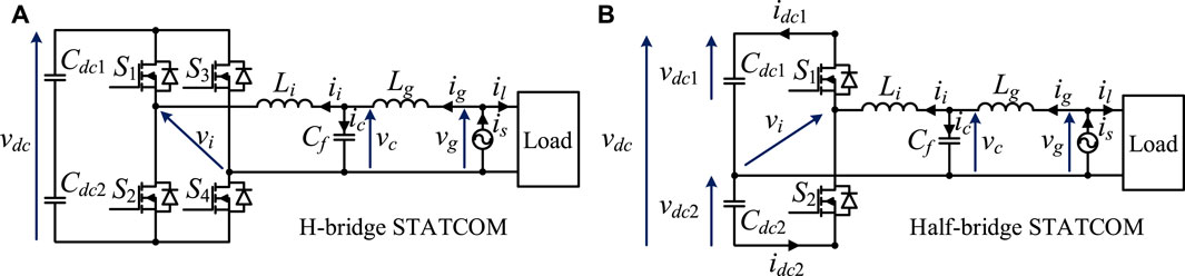
FIGURE 1. Circuit diagrams of single-phase (A) H-bridge and (B) half-bridge DSTATCOMs.
Assuming that the waveform of vg is an ideal sinusoidal with fundamental frequency fo and angular frequency ωo, it can be represented as
where Vg stands for the root-mean-square (rms) value of vg. In most cases, DSTATCOMs are employed to compensate for the reactive power absorbed by inductive or resistive-inductive loads. Under such conditions, the load current il lags vg by an angle θ, and it can be expressed as
where Il stands for the rms value of il, and Ilp and Ilq can be, respectively, derived as
From the equation (Singh et al., 2014), it can be observed that ilp is the active current component of il which is in phase with vg, and ilq denotes the reactive current component of il which is orthogonal to vg. In theory, ig should be equivalent to −ilq when the power losses in the DSTATCOM system are neglected, which can be represented as
Power flow analysis of single-phase H-bridge DSTATCOMs
The instantaneous power absorbed by the DSTATCOM can be calculated as
Normally, for LCL filters, the reactive power consumed by the filter inductors and capacitors is designed to be small enough as compared with the equipment rated power (Liserre et al., 2005; Fang et al., 2017a). Assuming that the power losses of these filter elements can be ignored, the instantaneous power absorbed by the DC-link capacitors pdc should be the same as pac, which can be expressed as
In order to absorb the fluctuating power pdc, the DC-link voltage vdc contains both a DC component and an AC component, which can be represented as
where Vdc and
Under this condition, the relevant power absorbed in the DC link, denoted as pdch, can be derived as
where the DC-link capacitances Cdc1 and Cdc2 in Figure 1 are chosen to be identical and denoted as Cdc. Comparing the equations by (Inzunza and Akagi, 2005) and (Kumar and Mishra, 2014a), α = −90° can be obtained. Furthermore, it is clear that pdch and pdc are not equal due to the additional fluctuating power of frequency 4fo in pdch caused by the interaction between
Figure 1B shows the circuit diagram of a conventional single-phase half-bridge DSTATCOM. In comparison with the single-phase H-bridge DSTATCOM, two semiconductor switches can be saved for the half-bridge DSTATCOM. As shown in Figure 1B, the power absorbed by the half-bridge DSTATCOM can be represented as that of the H-bridge DSTATCOM expressed in the equation by Akagi (2011) and the equation by Kumar and Mishra (2014a) due to the same reactive power compensation requirement.
In Figure 2, the DC-link voltage vdc is composed of both the upper arm capacitor voltage vdc1 and lower arm capacitor voltage vdc2, and it can be expressed as
where Vdci and
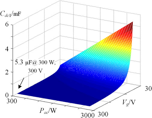
FIGURE 2. Cdc1 as a function of Vg and Pac under the reactive power decoupling operating condition.
It should be noted that the filter capacitor current ic is assumed to be zero in the equation by Karanki et al. (2012) to simplify the analysis. Based on the equation by Karanki et al. (2012), the difference between vdc1 and vdc2 can be derived as
where the DC-link capacitances Cdc1 and Cdc2 in Figure 2 are chosen to be identical and denoted as Cdc1. Furthermore, if the DC-link voltage vdc can be maintained as a constant DC value, the following equation can be satisfied:
Under this condition, the power absorbed in the DC link, denoted as pdcf, can be derived as
Under the condition that pdcf = pdc, the DC-link capacitance can be derived as
From the aforementioned analysis, for single-phase half-bridge DSTATCOMs, it is possible to regulate the DC-link voltage vdc to be constant and free of voltage harmonics under the rated operating condition by selecting Cdc1 properly. However, the fundamental voltage components in vdc1 and vdc2 may lead to overmodulation, and they can only be reduced with a larger Cdc1, according to the equation by Solanki et al. (2015). Therefore, it can be concluded that a constant DC-link voltage requires additional capacitors inserted in the individual arm to maintain the power balance between the DSTATCOM and the power grid. Cdc1 as a function of Vg and Pac under the reactive power decoupling operating condition is shown in Figure 2. As shown, Cdc1 under the complete power decoupling condition increases with the increase of Pac and decrease of Vg.
The circuit diagram of the proposed LCL-filtered half-bridge DSTATCOM is shown in Figure 3A. As can be observed, two additional capacitors Cdc3 and Cdc4 are adopted in the DC link to counteract voltage fluctuation. Furthermore, the filter capacitor Cf shown in Figure 2 is saved. The power absorbed by this novel half-bridge DSTATCOM can also be represented by the equation by Akagi (2011) and Kumar and Mishra (2014a). Furthermore, equation (Karanki et al., 2012)-(14) still holds true.
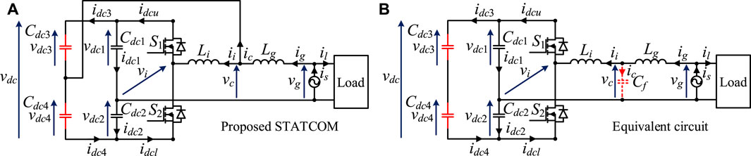
FIGURE 3. Circuit diagrams of (A) the proposed LCL-filtered half-bridge DSTATCOM and (B) its equivalent circuit.
Different from the conventional half-bridge DSTATCOM, Cdc3 and Cdc4 shown in Figure 4 can further absorb the reactive power, represented as
where pdca denotes the reactive power absorbed by Cdc3 and Cdc4.
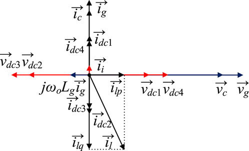
FIGURE 4. Vector diagram of the proposed half-bridge DSTATCOM. Equivalent LCL filter and the controller structure of the proposed half-bridge DSTATCOM.
The AC voltage components across Cdc3 and Cdc4 can be derived from Figure 3A and (Solanki et al., 2015), which can be described as
The currents flowing through Cdc3 and Cdc4, denoted as idc3 and idc4, respectively, can be derived based on the derivation relationship between the capacitor voltages and capacitor currents, which can be expressed as
where the additional capacitances Cdc3 and Cdc4 are chosen to be identical and denoted as Cdc3. It should be noted that the DC components Vdc3 of vdc3 and Vdc4 of vdc4 have no contribution to idc3 and idc4. Furthermore, pdca shown in the equation by Tang et al. (2015a) will not be influenced by Vdc3 and Vdc4 due to the opposite directions of idc3 and idc4. Substituting the equations by Shimizu et al. (1997) and Farivar et al. (2015) into the equation by Tang et al. (2015a) and solving for Cdc3,
From the equation by Tang et al. (2015b), Cdc3 can be calculated based on Cdc1 and the rated operating point of DSTATCOM systems. The system vector diagram is shown in Figure 4 to illustrate the relationships among all the voltage vectors and current vectors. As can be observed,
The equivalent LCL filter of the proposed half-bridge DSTATCOM is shown in Figure 3B. Based on Figure 3, the equivalent filter capacitance Cf can be derived as
where Cdc2 and Cdc4 are selected to be the same as Cdc1 and Cdc3, respectively.
The resonant frequency fr of the equivalent LCL filter can be derived as
Normally, for LCL filters, the filter capacitance Cf is selected to be several µF (6–8). The reason for choosing such small values is that larger capacitances increase the reactive component of the converter current ii and the system costs and volumes. However, for the proposed half-bridge DSTATCOM, the magnitude of ii can be reduced with a larger Cf, as shown in Figure 4, and Cf composed of Cdc1, Cdc2, Cdc3, and Cdc4 can be a relatively large value. When fr remains fixed, one direct advantage of using a larger Cf is the reduction in filter inductances. The inductance Li should be determined by the converter ripple current requirement (Wu et al., 2012), which can be represented as
where ΔIi denotes the peak value of the current ripple flowing through the inductor Li. Consequently, the grid-side inductance Lg can be greatly reduced to maintain a fixed fr (Jalili and Bernet, 2006; Tang et al., 2012).
The control block diagram of the proposed half-bridge DSTATCOM is shown in Figure 5. Figure 5A shows the reactive current detection and voltage-loop controller. A phase-locked loop (PLL) is utilized to synchronize the phase of vg for d-q transformation (Blaabjerg et al., 2006; Singh and Solanki, 2009). The fundamental active component of il is extracted first by multiplying sin ωt with il and then filtered through a low-pass filter (LPF) with a gain of 2. vdc* represents the reference voltage of vdc, which is regulated by a voltage-loop proportional-integral (PI) controller. It should be noted that igref would contain a considerable third-order harmonic, provided that the second-order voltage harmonic in vdc is large (Tang et al., 2015a; Tang et al., 2015b). The z-domain control block diagram of the current-loop controller can be observed from Figure 5B. In Figure 5B, Gi(z) denotes the z-domain current-loop controller, and z−1 is introduced by the computational delay of digital microprocessors (Pan et al., 2014; Parker et al., 2014; Van de Sype et al., 2016).
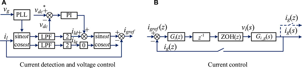
FIGURE 5. Control block diagrams of the proposed half-bridge DSTATCOM. (A) Current detection and voltage control and (B) Current control.
The transfer function ZOH(z) represents the effect of zero-order hold (ZOH), and the converter output voltage vi(s) can be obtained after the ZOH. Gi_g(s) stands for the transfer function from vi(s) to ig(s), as shown in Figure 5B, which can be derived as
where ωr = 2π fr represents the resonant angular frequency. The z domain transfer function Gi_g(z) can be derived from the equation by Tang et al. (2012) using the z transform with ZOH, and Gi_g(z) can be expressed as
where Ts = 1/fs denotes the sampling period, and Lt stands for the sum of Li and Lg. Based on the equation by Jalili and Bernet (2006) and Figure 5, the z domain loop gains of the current-loop can be derived as
It can be observed that the system mathematical model derived previously is similar to that of grid-current feedback LCL-filtered grid-connected converters (Wang et al., 2016b). Therefore, the controllers shown in Figure 7 can be designed based on the existing design methods, as provided in Bao et al. (2014), Zou et al. (2014), and Wang et al. (2016b). A proportional gain Kp is used as Gi (z) in the following section for simplifying the analysis.
The passive components shown in Figure 3, including the filter inductances Li and Lg and DC-link capacitances Cdc1–Cdc4 will be designed in this section. Before designing these parameters, the DSTATCOM system parameters should be provided, which include the fundamental frequency fo, sampling frequency fs, switching frequency fsw, grid voltage rms value Vg, rated reactive current rms value Ilq, and DC-link voltage reference vdc*.
With the system parameter values given, a step-by-step passive component design flowchart is shown in Figure 6. As can be observed, the first step is to specify
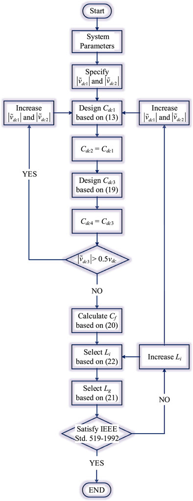
FIGURE 6. Passive components’ design flowchart.

TABLE 1. System parameter values for the experiments.
As can be obtained from Table 1, the grid-side filter inductance Lg is much smaller than that of the conventional LCL filter (Liserre et al., 2005; Jalili and Bernet, 2006; Channegowda and John, 2010; Bao et al., 2012; Liu et al., 2014; Fang et al., 2017b), leading to lower costs and power losses. In addition, it should be noted that capacitances Cdc1–Cdc4 listed in Table 1 are slightly different from theoretical calculated values, considering that the DSTATCOM system is implemented with standard capacitances; however, the differences are maintained within 10%. In Table 1, Kpv and Kiv represent the proportional gain and integral gain of the voltage-loop controller, respectively.
The Bode diagram and root locus of Ti(z) with the parameter values listed in Table 1 are shown in Figure 7. As can be observed from Figures 7A, the gain margin (GM) of 4.63 dB and phase margins (PM) greater than 40° can be obtained with a 700-Hz current-loop crossover frequency, indicating the satisfactory dynamic response of the current-loop controller (Bao et al., 2012; Pan et al., 2014). Furthermore, as verified by the locations of closed-loop poles shown in Figure 7B, the system stable margin is large enough to tackle the uncertainties introduced by component tolerance (Dannehl et al., 2010a; Dannehl et al., 2010b).
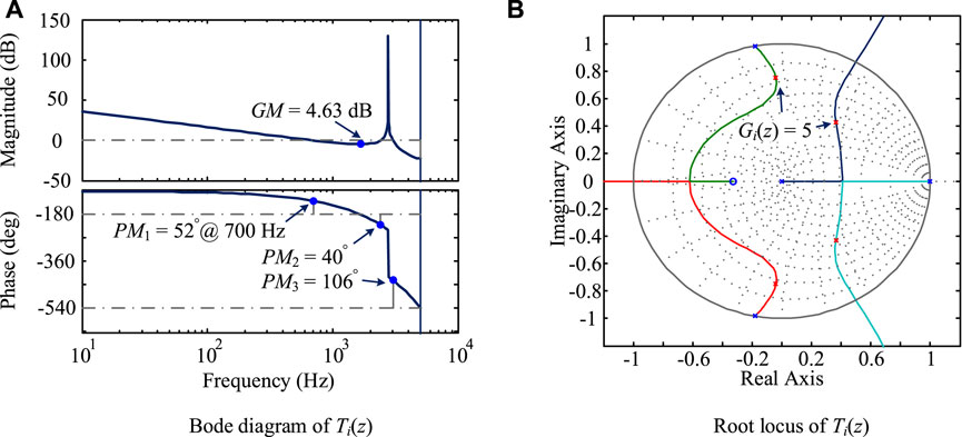
FIGURE 7. Bode diagram and root locus of Ti(z) with system parameters listed in Table 1. (A) Bode diagram Ti(z). (B) Root locus of Ti(z).
The simulation models of the conventional single-phase half-bridge DSTATCOM, single-phase H-bridge DSTATCOM, and proposed single-phase half-bridge DSTATCOM were constructed based on the MATLAB/Simulink software, and the relevant simulation parameter values are listed in Table 2. In Table 2, the DC-link capacitances of conventional and proposed half-bridge DSTATCOMs are selected using the equation by Kumar and Mishra (2015) and Figure 6, respectively. Moreover, the DC-link equivalent capacitance of the H-bridge DSTATCOM is chosen to be equivalent to that of the proposed DSTATCOM.
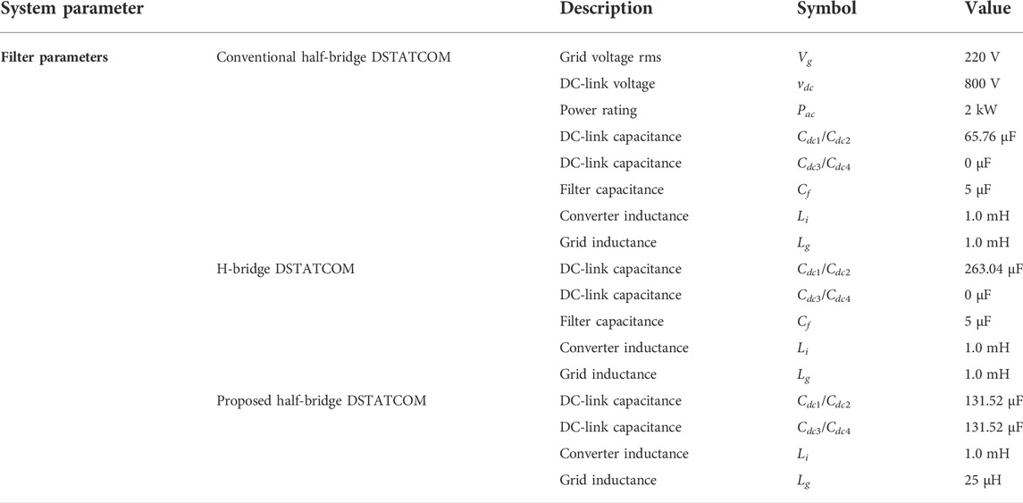
TABLE 2. Simulation parameter values.
The simulation results of the conventional half-bridge DSTATCOM are shown in Figure 8A. As shown, although the DC-link capacitances of the conventional half-bridge DSTATCOM are smaller, the voltage across each DC-link capacitor, namely, vdc1 and vdc2, varies in a wide range. At its minimum value, vdc1 or vdc2 may drop below 200 V, which is lower than 2/3 of the peak value of vg, leading to overmodulation of the PWM converter. Furthermore, the distorted waveforms of the compensating current ig and source current is can be observed from Figures 10A,B; 6.26% THD of is can be obtained (through FFT analysis), which obviously violates the grid code (IEEE, 1992).
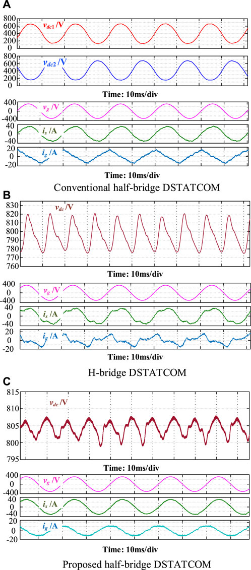
FIGURE 8. Simulation waveforms of the conventional half-bridge, H-bridge, and proposed half-bridge DSTATCOMs. (A) Conventional half-bridge DSTATCOM. (B) H-bridge DSTATCOM. (C) Proposed half-bridge DSTATCOM.
The simulation waveforms of the conventional H-bridge DSTATCOM are illustrated in Figure 8B. As shown in Figure 8B, the DC-link voltage vdc fluctuates with considerable second-order harmonics and other even-order harmonics. These voltage harmonics deteriorate the grid current. As a consequence, the THD of is was found to be 17.04%, which is far from satisfactory levels of the grid code.
The simulation waveforms of the proposed half-bridge DSTATCOM are shown in Figure 8C. With carefully designed DC-link capacitances, the variation of vdc is maintained within 10 V. The waveform of is becomes sinusoidal with a THD of 3.88%, indicating compliance with the grid code.
A single-phase half-bridge DSTATCOM experimental prototype was built and tested in the laboratory, whose schematic diagram is depicted in Figure 3. The system parameters used in the experiments are listed in Table 3, and the relevant controller structures are shown in Figure 5. The control algorithm was executed on a dSPACE control platform (DS1103). Litz wires were utilized for filter inductor windings to minimize their ESRs. Filter capacitors are film capacitors instead of electrolytic capacitors, which are combined with DC-link capacitors. It is clear from the experimental parameters (listed in Table 3) that capacitances are small, which is only 470 μF. The power grid was emulated by a programmable AC power supply (Chroma 61,502), and all the experimental waveforms were captured from a digital oscilloscope (MSO 44MXs-B). SiC MOSFETs (C3M0065090D) with low power losses were employed as S1 and S2 switched complementarily with a 1-µs dead time inserted.
TABLE 3. Parameter values of the conventional LCL filtered half-bridge DSTATCOM.
Before enabling the proposed half-bridge DSTATCOM, a 22-mH inductance Ll connected in parallel with a 10 Ω resistance Rl served as the load. The load current lags the grid voltage by 75° approximately.
Figure 9 shows the experimental waveforms with the reactive power compensated by the proposed half-bridge DSTATCOM. As can be observed, the DC-link voltage vdc has been regulated to the reference value of 200 V. In addition, ig leads vg about 90°, indicating that ig is mainly composed of the capacitive reactive current. It should be noted that ig also contains an active current component, whose magnitude is much smaller than that of the capacitive reactive current. The active current component is necessary to maintain a constant DC-link voltage and compensate for the power losses. After the reactive power compensation, the source current is comes in phase with vg, indicating that the power factor observed from the power grid has been improved to unity. Furthermore, as verified by Figure 9, the converter current ii is much lower than ig, as has been discussed in Section 3 B. Figure 9 also shows the experimental waveforms of capacitor voltages vdc1–vdc4 with the proposed half-bridge DSTATCOM enabled. As can be noticed, the DC components of vdc1–vdc4 are the same and equals to 100 V. The AC components of vdc1, vdc4, and is are all in phase, as proved by Figure 4. Moreover, the AC components of vdc2 and vdc3 are in the opposite direction to vdc1 and vdc4, respectively, which proves that the required reactive power is compensated by all the four capacitors.
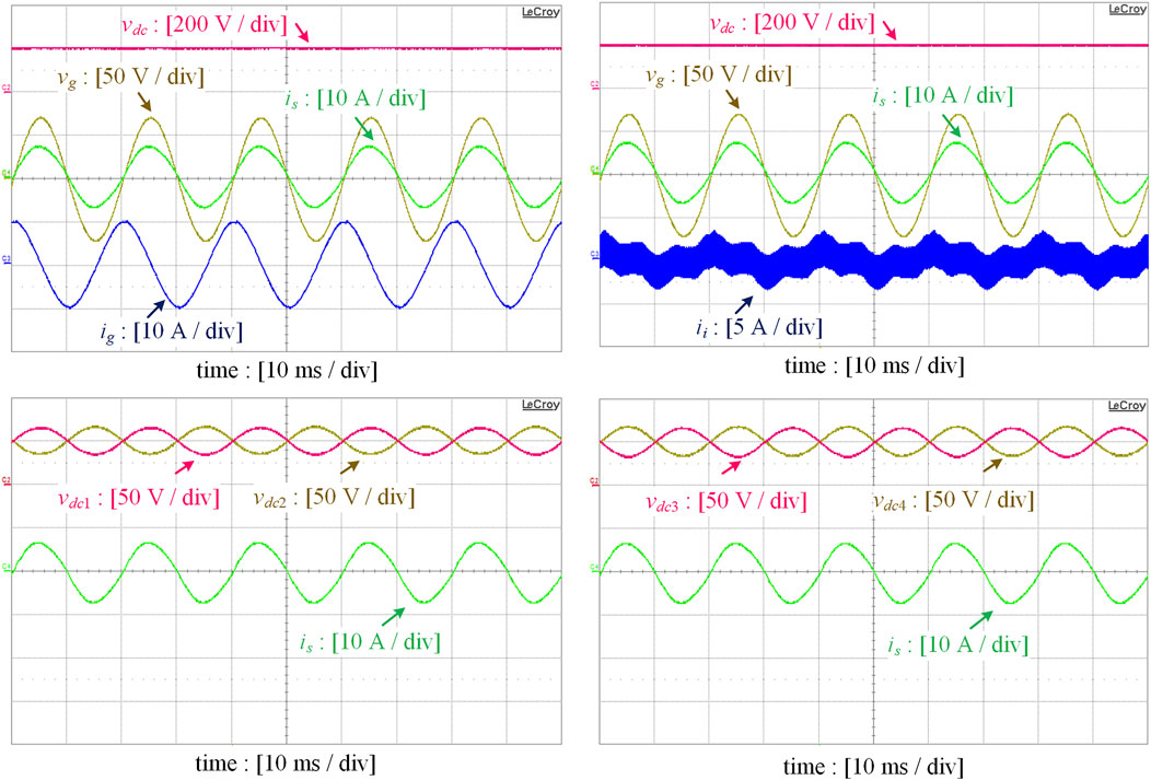
FIGURE 9. Experimental waveforms with reactive power compensated by the proposed DSTATCOM.
Figure 10 illustrates the experimental waveforms when the proposed half-bridge DSTATCOM is enabled with a light load, composed of a 22-mH inductance Ll connected in series with a 10 Ω resistance Rl. Before compensation, is is a resistive–capacitive current that leads vg by approximately 60°, which is mainly composed of the reactive current absorbed by Cdc1–Cdc4. After the proposed half-bridge DSTATCOM is put into operation under the light load condition, the reactive current absorbed by the proposed DSTATCOM can be regulated to the reference value, and as a result is comes in phase with vg. Once again, the DC-link voltage vdc can be maintained as a reference value of 200 V.
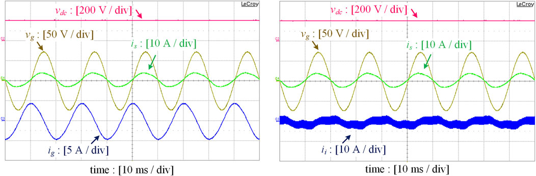
FIGURE 10. Experimental waveforms with reactive power compensated by the proposed DSTATCOM under light load condition.
Figure 11 shows the experimental waveforms when the reactive power is compensated by a conventional LCL-filtered half-bridge DSTATCOM. All the DC-link capacitances remain the same as those listed in Table 1, and parameter values of the LCL filter are provided in Table 2.
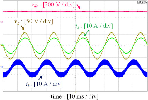
FIGURE 11. Experimental waveforms with reactive power compensated by the conventional LCL-filtered half-bridge DSTATCOM.
It can be observed that a larger inductor Lg and an additional capacitor Cf are added to form the LCL filter, as shown in Figure 2. Furthermore, the load inductance Ll has been intentionally reduced from 22 to 12 mH in order to decrease the magnitude of reactive current ig. The reason is that is and vg may have a phase difference due to the limited compensation ability of controllers provided that the same load as that adopted in Figure 10 is used. As can be observed from Figure 11, the magnitude of ii becomes larger than that of ig and is, leading to increased current stress and power losses. In this case, the overmodulation of power converters will not be observed due to small power ratings. In addition, the third-order current harmonic can be attenuated to be less than 3% of Ilp with an additional 100 Hz second-order notch filter inserted into the voltage-loop PI controller.
The experimental results of the dynamic response of the proposed half-bridge DSTATCOM are provided in Figure 12. As can be observed, ig can be stabilized after 2–3 cycles of the sudden load change, indicating that the dynamic performance of the proposed controllers is satisfactory. The aforementioned experimental results agree well with the theoretical analysis.
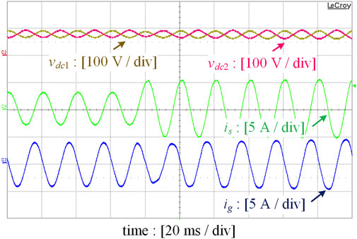
FIGURE 12. Experimental waveforms of the dynamic response of the proposed half-bridge DSTATCOM.
In this study, the novel LCL-filtered half-bridge DSTATCOM topology has been proposed. With the proposed half-bridge DSTATCOM, it is possible to regulate the DC-link voltage as a constant DC value without any fluctuations. Furthermore, the filter capacitor of the LCL filter can be replaced by the DC-link capacitors and hence be saved. Moreover, the currents flowing through the converter side inductance and semiconductor switches can be dramatically decreased, leading to lower power losses and current stresses of the switching devices. Another prominent advantage of the proposed half-bridge DSTATCOM is that its grid-side inductance can be greatly reduced from the order of millihenry to several microhenries. Following the passive component design procedure introduced in this study, the voltage fluctuation across each DC-link capacitor can be maintained within the predetermined limitation values, preventing the overmodulation caused by uncontrollable DC-link voltage fluctuations. A down-scaled prototype of the proposed half-bridge DSTATCOM was built and tested in the laboratory, and the experimental results are provided to validate the feasibility and correctness of the theoretical analysis.
The original contributions presented in the study are included in the article/Supplementary Material; further inquiries can be directed to the corresponding author.
JF came up with the raw idea of this novel LCL-filtered half-bridge DSTATCOM topology and instructed the simulations and the experiments. XM carried out the detailed analysis on this proposed topology and finished simulation and experiment verification.
The authors declare that the research was conducted in the absence of any commercial or financial relationships that could be construed as a potential conflict of interest.
All claims expressed in this article are solely those of the authors and do not necessarily represent those of their affiliated organizations, or those of the publisher, the editors, and the reviewers. Any product that may be evaluated in this article, or claim that may be made by its manufacturer, is not guaranteed or endorsed by the publisher.
Akagi, H. (2011). Classification, terminology, and application of the modular multilevel cascade converter (MMCC). IEEE Trans. Power Electron. 26, 3119–3130. doi:10.1109/IPEC.2010.5543243
Bao, C., Ruan, X., Wang, X., Li, W., Pan, D., Weng, K., et al. (2012). Design of injected grid current regulator and capacitor-current-feedback active- damping for LCL-type grid-connected inverter. Proc. IEEE Energy Conver. Congr. Expo. 29, 579–586. doi:10.1109/ECCE.2012.6342769
Bao, C., Ruan, X., Wang, X., Li, W., Pan, D., Weng, K., et al. (2014). Step-by-step controller design for LCL-type grid-connected inverter with capacitor-current-feedback active-damping. IEEE Trans. Power Electron. 29, 1239–1253. doi:10.1109/TPEL.2013.2262378
Blaabjerg, F., Teodorescu, R., Liserre, M., and Timbus, A. (2006). Overview of control and grid synchronization for distributed power generation systems. IEEE Trans. Ind. Electron. 53, 1398–1409. doi:10.1109/TIE.2006.881997
Channegowda, P., and John, V. (2010). Filter optimization for grid interactive voltage source inverters. IEEE Trans. Ind. Electron. 57, 4106–4114. doi:10.1109/tie.2010.2042421
Dannehl, J., Fuchs, F., Hansen, S., and Thøgersen, P. (2010). Investigation of active damping approaches for PI-based current control of grid-connected pulse width modulation converters with LCL filters. IEEE Trans. Ind. Appl. 46, 1509–1517. doi:10.1109/TIA.2010.2049974
Dannehl, J., Fuchs, F., and Thøgersen, P. (2010). PI state space current control of grid-connected PWM converters with LCL filters. IEEE Trans. Power Electron. 25, 2320–2330. doi:10.1109/TPEL.2010.2047408
Dugan, R., McGranaghan, M., Santoso, S., and Beaty, H. (2004). Electrical power systems quality. USA: McGraw-Hill.
Fang, J., Li, H., and Tang, Y. (2017). A magnetic integrated LLCL filter for grid-connected voltage source converters. IEEE Trans. Power Electron. 32, 1725–1730. doi:10.1109/TPEL.2016.2613578
Fang, J., Xiao, G., Yang, X., and Tang, Y. (2017). Parameter design of a novel Series-Parallel-Resonant LCL filter for single-phase half-bridge active power filters. IEEE Trans. Power Electron. 32, 200–217. doi:10.1109/TPEL.2016.2532961
Farivar, G., Hredzak, B., and Agelidis, V. (2015). Reduced-capacitance thin-film H-bridge multilevel STATCOM control utilizing an analytic filtering scheme. IEEE Trans. Ind. Electron. 62, 6457–6468. doi:10.1109/tie.2015.2420675
IEEE (1992). IEEE recommended practices and requirements for harmonic control in electric power systems. IEEE Stand. 1992, 519. doi:10.1109/IEEESTD.1993.114370
Inzunza, R., and Akagi, H. (2005). A 6.6-kV transformerless shunt hybrid active filter for installation on a power distribution system. IEEE Trans. Power Electron. 20, 893–900. doi:10.1109/TPEL.2005.850951
Isobe, T., Shiojima, D., Kato, K., Hernandez, Y., and Shimada, R. (2016). Full-bridge reactive power compensator with minimized-equipped capacitor and its application to static var compensator. IEEE Trans. Power Electron. 31, 224–234. doi:10.1109/TPEL.2015.2412954
Jalili, K., and Bernet, S. (2006). Design of LCL filters of active-front-end two level voltage-source converters. IEEE Trans. Ind. Electron. 56, 1674–1689. doi:10.1109/TIE.2008.2011251
Karanki, S., Geddada, N., Mishra, M., and Kumar, B. (2012). A DSTATCOM topology with reduced DC-link voltage rating for load compensation with nonstiff source. IEEE Trans. Power Electron. 27, 1201–1211. doi:10.1109/TPEL.2011.2163946
Kumar, C., and Mishra, M. (2014). A multifunctional DSTATCOM operating under stiff source. IEEE Trans. Ind. Electron. 61, 3131–3136. doi:10.1109/TIE.2013.2276778
Kumar, C., and Mishra, M. (2014). An improved hybrid DSTATCOM topology to compensate reactive and nonlinear loads. IEEE Trans. Ind. Electron. 61, 6517–6527. doi:10.1109/TIE.2014.2321355
Kumar, C., and Mishra, M. (2015). Operation and control of an improved performance interactive DSTATCOM. IEEE Trans. Ind. Electron. 62, 6024–6034. doi:10.1109/TIE.2015.2420635
Liang, Y., and Nwankpa, C. (1999). A new type of STATCOM based on cascading voltage-source inverters with phase-shifted unipolar SPWM. IEEE Trans. Ind. Appl. 35, 1118–1123. doi:10.1109/28.793373
Liserre, M., Blaabjerg, F., and Hansen, S. (2005). Design and control of an LCL filter-based three-phase active rectifier. IEEE Trans. Ind. Appl. 41, 1281–1291. doi:10.1109/TIA.2005.853373
Liu, Q., Peng, L., Kang, Y., Tang, S., Wu, D., Qi, Y., et al. (2014). A novel design and optimization method of an LCL filter for a shunt active power filter. IEEE Trans. Ind. Electron. 61, 4000–4010. doi:10.1109/TIE.2013.2282592
Pan, D., Ruan, X., Bao, C., Li, W., and Wang, X. (2014). Capacitor-current-feedback active damping with reduced computation delay for improving robustness of LCL-type grid-connected inverter. IEEE Trans. Power Electron. 29, 3414–3427. doi:10.1109/TPEL.2013.2279206
Parker, S., McGrath, B., and Holmes, D. (2014). Regions of active damping control for LCL filters. IEEE Trans. Ind. Appl. 50, 424–432. doi:10.1109/TIA.2013.2266892
Peng, F., Lai, J., McKeever, J., and VanCoevering, J. (1996). A multilevel voltage-source inverter with separate DC sources for static var generation. IEEE Trans. Ind. Appl. 32, 1130–1138. doi:10.1109/IAS.1995.530626
Shimizu, T., Fujita, T., Kimura, G., and Hirose, J. (1997). A unity power factor PWM rectifier with DC ripple compensation. IEEE Trans. Ind. Electron. 44, 447–455. doi:10.1109/41.605618
Singh, B., Jayaprakash, P., Kothari, D., Chandra, A., and Haddad, K. (2014). Comprehensive study of DSTATCOM configurations. IEEE Trans. Ind. Inf. 10, 854–870. doi:10.1109/tii.2014.2308437
Singh, B., and Solanki, J. (2009). A comparison of control algorithms for DSTATCOM. IEEE Trans. Ind. Electron. 56, 2738–2745. doi:10.1109/TIE.2009.2021596
Solanki, J., Fröhleke, N., and Böcker, J. (2015). Implementation of hybrid filter for 12-Pulse thyristor rectifier supplying high-current variable-voltage DC load. IEEE Trans. Ind. Electron. 62, 4691–4701. doi:10.1109/TIE.2015.2393833
Tang, Y., and Blaabjerg, F. (2015). A component-minimized single-phase active power decoupling circuit with reduced current stress to semiconductor switches. IEEE Trans. Power Electron. 30, 2905–2910. doi:10.1109/TPEL.2014.2369959
Tang, Y., Blaabjerg, F., Loh, P., Jin, C., and Wang, P. (2015). Decoupling of fluctuating power in single-phase systems through a symmetrical half-bridge circuit. IEEE Trans. Power Electron. 30, 1855–1865. doi:10.1109/TPEL.2014.2327134
Tang, Y., Loh, P., Wang, P., Choo, F., Gao, F., Blaabjerg, F., et al. (2012). Generalized design of high performance shunt active power filter with output LCL filter. IEEE Trans. Ind. Electron. 59, 1443–1452. doi:10.1109/TIE.2011.2167117
Tang, Y., Qin, Z., Blaabjerg, F., and Loh, P. (2015). A dual voltage control strategy for single-phase PWM converters with power decoupling function. IEEE Trans. Power Electron. 30, 7060–7071. doi:10.1109/tpel.2014.2385032
Van de Sype, D., Gusseme, K., De Belie, F., Bossche, A., and Melkebeek, J. (2016). Small-signal z-domain analysis of digitally controlled converters. IEEE Trans. Power Electron. 21, 470–478. doi:10.1109/TPEL.2005.869758
Wang, J., Yan, J., Jiang, L., and Zou, J. (2016). Delay-dependent stability of single-loop controlled grid-connected inverters with LCL Filters. IEEE Trans. Power Electron. 31, 743–757. doi:10.1109/TPEL.2015.2401612
Wang, L., Lam, C., and Wong, M. (2016). A hybrid-STATCOM with wide compensation range and low DC-link voltage. IEEE Trans. Ind. Electron. 63, 3333–3343. doi:10.1109/TIE.2016.2523922
Wang, X., Pang, Y., Loh, P., and Blaabjerg, F. (2015). A series-LC-filtered active damper with grid disturbance rejection for ac power-electronics-based power systems. IEEE Trans. Power Electron. 30, 4037–4041. doi:10.1109/TPEL.2014.2382477
Wu, W., He, Y., and Blaabjerg, F. (2012). An LLCL power filter for single-phase grid-tied inverter. IEEE Trans. Power Electron. 27, 782–789. doi:10.1109/TPEL.2011.2161337
Keywords: DC-link capacitors, distributed static compensators, half-bridge, LCL filter, power quality
Citation: Meng X and Fang J (2022) A half-bridge distributed static compensator with a DC-link filter capacitor of a reduced size LCL filter. Front. Energy Res. 10:929676. doi: 10.3389/fenrg.2022.929676
Received: 27 April 2022; Accepted: 15 July 2022;
Published: 23 August 2022.
Edited by:
Thomas Bartzanas, Agricultural University of Athens, GreeceReviewed by:
Yitao Liu, Shenzhen University, ChinaCopyright © 2022 Meng and Fang. This is an open-access article distributed under the terms of the Creative Commons Attribution License (CC BY). The use, distribution or reproduction in other forums is permitted, provided the original author(s) and the copyright owner(s) are credited and that the original publication in this journal is cited, in accordance with accepted academic practice. No use, distribution or reproduction is permitted which does not comply with these terms.
*Correspondence: Jingyang Fang, amluZ3lhbmdmYW5nQHNkdS5lZHUuY24=
Disclaimer: All claims expressed in this article are solely those of the authors and do not necessarily represent those of their affiliated organizations, or those of the publisher, the editors and the reviewers. Any product that may be evaluated in this article or claim that may be made by its manufacturer is not guaranteed or endorsed by the publisher.
Research integrity at Frontiers
Learn more about the work of our research integrity team to safeguard the quality of each article we publish.