
95% of researchers rate our articles as excellent or good
Learn more about the work of our research integrity team to safeguard the quality of each article we publish.
Find out more
BRIEF RESEARCH REPORT article
Front. Energy Res. , 29 June 2022
Sec. Smart Grids
Volume 10 - 2022 | https://doi.org/10.3389/fenrg.2022.922786
This article is part of the Research Topic Highly Efficient and Reliable Power Converters for Microgrid Applications View all 6 articles
 Narayanan Pandurangan Gopinath*
 Krishnasamy Vijayakumar
The article discusses a nine-level switching capacitor-based common ground-type boost inverter for grid-connected photovoltaic applications. The proposed structure’s direct connection between the negative terminal of the input source and the grid neutral eliminates leakage current. The proposed topology uses eleven switches, two diodes, and three switching capacitors to produce a double voltage boost with nine different voltage levels. Self-balancing switching capacitors eliminate the need for sophisticated independent control algorithms. The maximum voltage stress on one of the three capacitors equals the input voltage, while it is equal to half of the input voltage on the other two switched capacitors. The various modes of operation and capacitance calculation are discussed in depth. A comprehensive comparison with various nine-level topologies has been conducted in terms of total component count, total standing voltage, capacitor voltage, and approximate cost to demonstrate the proposed topology’s benefits. A 400-W inverter prototype is constructed, and the experimental findings under various operating situations are reviewed.
Transformerless inverters (TLIs) for photovoltaic (PV) technology are gaining more popularity due to their simple structure, absence of a transformer, smaller size, reduced weight, and higher efficiency (Islam et al., 2015). The absence of a transformer removes the galvanic isolation between the PV array and the grid, resulting in leakage current through the parasitic capacitance between the PV source and the ground (González et al., 2008; Li et al., 2015). The undesirable leakage current causes many issues related to personnel safety, degrading the PV array characteristics, increased current harmonic distortion, and electromagnetic interference (Sonti et al., 2017). Therefore, it is mandatory to address the leakage current issue in the non-galvanic inverters. Thus, many approaches have been made based on novel topology derivations, new control algorithms, and different pulse modulation schemes to minimize the leakage current (Khan et al., 2020). From the topological point of view, the TLIs mitigate the leakage current using any one of the following methods: 1) decoupling the source from the grid, 2) connecting the grid neutral to the midpoint of the DC link, and 3) direct connection of the source negative terminal with the grid neutral, i.e., both connecting points are at ground potential (Kumari et al., 2021c). The TLIs derived from conventional full bridge (FB) can mitigate the leakage current by decoupling the source and load on the DC side (DC decoupling) or on the AC side (AC decoupling) during the freewheeling mode. In DC decoupling, the high switching stress of the H5 topology (Victor et al., 2008) is shared by two power switches employed on the positive and negative buses, known as the H6 topology (Islam and Mekhilef, 2015). An AC decoupling topology with a highly efficient and reliable inverter concept (HERIC) is presented in Heribert et al. (2003). However, in DC and AC decoupling methods, the TLIs fail to minimize the leakage current completely. Other drawbacks of decoupling type TLIs include increased conduction losses caused by extra power switches and an inability to meet grid voltage without a boost converter at the input side. Another approach to confront current is to connect the mid-point of the DC link capacitor to the grid neutral, known as neutral point clamped (NPC) or active neutral point clamped (ANPC) topologies (Zhang et al., 2013; Debnath and Chatterjee, 2016; Kumari M. et al., 2021). The requirement of an additional front-end DC–DC boost power processing stage to meet the AC grid amplitude is the main disadvantage of NPC-type topologies. In both topologies (Siddique et al., 2020; Siwakoti et al., 2020), an active neutral point clamped (ANPC) inverter with boosting capability is presented. Since the output of these topologies is equal to the input, they still need front-end boost converters when dealing with the low-voltage paralleled PV string panels. An effective alternative to suppress the leakage current is common ground (CG)-type topologies, in which the common ground is shared between the source and the neutral side of the grid, eliminating the common mode voltage. A CG topology using switched capacitors as a virtual bus is presented in Gu et al. (2013). The switched capacitor is charged during the positive half cycle, and it acts as a virtual source during the negative half cycle to supply load. Like a conventional full-bridge inverter, the maximum output voltage of this topology is the same as the input DC-link voltage. Some five-level inverter topologies (Kadam and Shukla, 2017; Grigoletto, 2020; Sandeep et al., 2020) are presented based on the common ground type, but they are incapable of boosting the input voltage. By adding a switched or flying capacitor to the CG-type structure, the output voltage can be boosted while generating a multi-level output voltage waveform. The topologies of Vosoughi et al. (2020), Kumari et al. (2021b), and Mohamed Ali et al. (2022) overcome the shortcomings of the preceding topologies by boosting the output voltage to twice the input voltage with reduced power components. The topologies of Shaffer et al. (2018) and Sathik et al. (2021) have a CG-type structure with a voltage gain of 2 and 4, respectively. The main drawback of these topologies is the utilization of a higher number of power components to generate five-level output voltage. The topology Habib Khan et al. (2020) can operate in both buck and boost modes to provide the same AC output voltage, but it has a large inrush current. In recent times, a common ground structure with more output voltage levels and high voltage gain has attained more focus among researchers. Thus, a seven-level CG structure (Grigoletto, 2021) with triple voltage gain and nine-level CG type (Chen et al., 2022) with quadruple voltage gain is presented. To generate a seven-level output voltage, the topology (Grigoletto, 2021) requires a total component count of sixteen, which significantly increases the power loss. The high voltage stress of three times the input voltage on five switches and on one capacitor is the main issue with the topology (Chen et al., 2022). By keeping all the aforementioned issues in the literature, this article presents a new common ground type nine-level inverter (CG9-L) topology with the following features:
i) Single phase, nine-level output voltage with integrated boost operation (voltage gain is 2).
ii) The maximum voltage stress on capacitor is equal to the input voltage.
iii) The maximum voltage stress is equal to the output voltage.
iv) Inherent capacitor voltage balancing.
v) Leakage current is suppressed because of the common ground structure.
This article is presented as follows: the proposed topology and its operation followed by capacitance calculation, power loss calculation, result discussion, comparative analysis with other existing MLI’s, and conclusion.
The proposed CG9-L circuit configuration is depicted in Figure 1A. Structurally, CG-9L is composed of eleven power switches (S1 to S9 and SB), three switched capacitors (C1, C2, and C3), and two diodes (Da and Db). The power switch SB is bidirectional, and all the other switches are unidirectional. The maximum voltage across the switched capacitor C1 is equal to the input voltage and that across the remaining two capacitors, C2 and C3, is equal to half of the input voltage. The proposed CG9-L design has an inherent voltage balancing feature, and thus, it does not require any additional control circuits or algorithms to maintain the voltage balance of the capacitors. The neutral of the load side and the negative terminal of the input DC source are connected to the ground to establish a common ground feature.
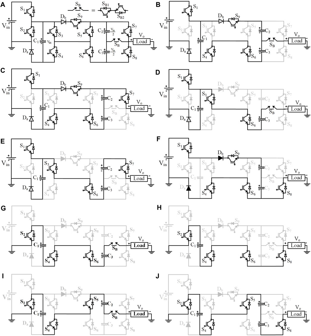
FIGURE 1. Topology and its modes of operation. (A)Proposed CG-9L topology, (B) Vo = 0.5Vin, (C) Vo = Vin, (D) Vo = 1.5Vin, (E) Vo = 2Vin, (F) Vo = 0, (G) Vo = −0.5Vin, (H) Vo = −Vin, (I) Vo = −1.5Vin, and (J) Vo = −2Vin.
The nine output voltage levels, namely, 0.5 Vin, Vin, 1.5 Vin, 2 Vin, 0, −0. 5Vin, −Vin, −1.5 Vin, and −2 Vin, are synthesized, as shown in Figures 1B–J. Based on the different modes of operation, the switched capacitors C1, C2, and C3 are charged and discharged during every switching cycle. The detailed description of all the operating states is given as follows:
The first positive output voltage level of the proposed topology is generated by turning on switches S1, S4, S6, S9, and SB to generate an output voltage level of 0.5Vin, as shown in Figure 1B. The load current completes its path through SB, the anti-parallel diode of switches S6 and S4, Da, and the negative terminal of the source. Here, the output voltage is positive, and the load current is negative. The capacitors C1 and C3 get charged during this mode of operation, and it is expressed as follows:
The input source is directly connected to the load through the power switches S1, S7, and S9, as shown in Figure 1C. The switches S4 and S6 are also turned on to charge the capacitors C2 and C3. Since all the three capacitors are connected in parallel with the input source during this mode of operation, they get charged. The capacitor voltage and output voltage are expressed as follows:
The power switches S1, S3, S6, and SB are switched ON, and output current is conducted. The input source and capacitor C3 voltages are added together to deliver the load, as shown in Figure 1D. Here, the capacitor C1 is charged, and C3 is discharged. Here, the output voltage is written as follows:
The proposed topology’s maximum output voltage level is obtained by turning on the switches S1, S3, S6, and S7, as shown in Figure 1E. During this mode, the input source and capacitor voltages VC2 and VC3 cumulatively deliver the load requirement. The capacitor C1 is connected in parallel with the input source and charged to Vin. The respective voltages are expressed as
In this mode, the power switches S4, S6, and S8 are switched ON to provide a freewheeling path for the load. As shown in Figure 1F, the switches S1 and S9 are turned ON to charge the capacitors C1, C2, and C3. The respective voltages are expressed as
The switches S2, S4, S6, and SB are triggered ON to generate an output voltage level of −0.5Vin, and the respective voltage level is shown in Figure 1G. Here, the output voltage is negative, and the load current is positive. The current flows through SB, the anti-parallel diode of switches S6, S4, C1, and S2, and the negative terminal of the source. The output voltage is expressed as follows:
Here, the power switches S2, S4, S6, and S8 are triggered ON, and the respective current flow path is shown in Figure 1H. The capacitor C1 is discharged to supply the load and it is written as follows:
The power switches S2, S4, S5, and SB are switched ON, and the load current is conducted. The capacitors C1 and C2 are discharging to deliver the load. The respective current flow path is shown in Figure 1I, and the output voltage is expressed as follows:
This mode of operation generates the negative maximum output voltage level, and the load current flow path is shown in Figure 1J. The power switches S2, S4, S5, and S8 are triggered ON. Here, all three capacitors are discharging to supply the load. The output voltage in this mode is written as
The three switched capacitors C1, C2, and C3 in the proposed CG9-L topology are self-balanced using a series-parallel technique (Siddique et al., 2019). The selection of the capacitance value of these capacitors is important in switched capacitor topologies to achieve the desired output voltage waveform. Also, it involves ripple loss, size, and total cost of the inverter. The longest discharging time of capacitors has been used to calculate the capacitance value. The capacitances are estimated by considering the maximum allowable ripple limit of 10% of its maximum voltage (Liu et al., 2014). The time period to calculate the capacitance value is written using a typical nine-level output voltage waveform as follows:
where To is the period of the output voltage waveform. The charge on the capacitors C1, C2, and C3 at the resistive load during its LDC period is estimated as follows:
The load current value for purely resistive load can be expressed as follows:
From Equations 10 and 12, the charge on the capacitor C1 during resistive load is estimated as
The optimum value of the capacitance of capacitor C1 when the load is purely resistive is calculated as
From Equations 11 and 12, the charge on the capacitors C2 and C3 during the resistive load is calculated as
The optimum value of the capacitance of capacitors C2 and C3 when the load is purely resistive can be calculated as
When the load is resistive-inductive (RL), the load current is expressed as follows:
At resistive-inductive (RL) loading conditions, the charge on the capacitance of capacitors C1, C2, and C3 is calculated as
The optimum value of the capacitance of capacitors C1, C2, and C3 during resistive-inductive (RL) loading can be written as follows:
where Imx is the maximum load current.
The total power loss of a topology depends on three losses: switching losses, conducting losses, and ripple losses. The overall efficiency can be estimated as
where
When a power switch transition happens, i.e., when turn ON to turn OFF or turn OFF to turn ON, voltage and current overlapping occurs (Babaei et al., 2014). This causes loss in the power switch called switching loss. The switching losses of each power switch during turning ON
where Vst-ON, Ist-ON, and TON are the voltage across the switch when it is turned ON, current through the power switch during ON period, and turn ON time of the power switch.
where Vst-OFF, Ist-OFF, and TOFF are the open circuit voltage of the switch when it is turned OFF, current through the power switch before turning OFF the power switch, and turn OFF time of the power switch, respectively. The total switching loss can be expressed as
The internal resistance of a power switch is the source of conduction losses when it is in conduction (Mohamed Ali et al., 2021). The total conduction loss is calculated using the equivalent circuit of the proposed CG9-L topology.
The conduction losses are estimated as
where
The total conduction loss is estimated as
The difference in voltage between the input DC source and the voltage across the capacitor causes capacitor ripple loss. The ripple voltage can be estimated as follows:
where ts-te is the start and end time duration of the longest discharge of the capacitor.
The ripple loss can be calculated (Ponnusamy et al., 2020) as
The total capacitor ripple loss can be calculated as follows:
The total loss of the proposed CG9-L can be calculated as follows:
The 400-W experimental prototype of the proposed CG-9L inverter is built in the laboratory using G60N100 IGBT switches, HCPL-3120 drivers, 1000 μF capacitors, Texas Instrument TMS320F28379D digital controller launchpad, and RL load, and its performance is analyzed under various steady-state and dynamic conditions. The switching frequency of the proposed inverter topology is 2.5 kHz. An input voltage of 100 V and load combinations of 100 Ω, 50 + j100 Ω, and 100 + j100 Ω were chosen while analyzing the performance of the proposed topology. The steady-state performance of a proposed topology has been analyzed by using a resistive load of 100 Ω, and the obtained experimental results of the output voltage, output current, and voltage across the capacitors are shown in Figures 2A–C. It is observed that the output voltage is 200 V while applying a 100 V input, which verifies the boosting ability of the proposed topology. The steady-state operating condition at a series resistive-inductive load of R = 100 and L = 100 mH with a power factor of 0.95 is also tested, and the results are shown in Figure 2D. The rms value of load current is 1.26 A, and the voltage across capacitors C1 and C2 is 100 and 50 V, respectively. The dynamic operating conditions such as input change, load change period, and variations in modulation index values have been checked. The experimental results of an output voltage that varies from 160 to 200 V and an output current that varies from 1.5 to 1.85 A when the input voltage is changed from 80 to 100 V are shown in Figure 3A. The load is changed from Z1 = 50 + j100Ω to Z2 = 100 + j100Ω to test the dynamic behavior. The output voltage is maintained at 200 V constantly, and the load current changes from 3.3 to 1.85 A. The corresponding results are shown in Figure 3C. Figure 3D shows the output voltage, current, capacitor voltage VC2, and capacitor current iC2 as the load is changed from R = 100 Ω to Z2 = 100 + j100 Ω. The waveform shows that the capacitor voltage remains stable when the load changes, verifying the capacitor’s self-voltage balancing ability. Furthermore, the change in modulation index values has also been analyzed, and the respective waveforms are shown in Figures 3E,F. The modulation index values are changed from 1 to 0.7 to 0.5. When the modulation index is 1, all nine voltage levels have been obtained. But when it is 0.7 and 0.5, the levels of output voltage are decreased to seven levels and five levels, respectively. During all these dynamic analyses, the capacitor voltages are maintained constantly with allowable ripple, confirming the self-balancing of capacitors. The inrush current that arises due to the direct parallel connection between the input source and the switched capacitor is reduced by the high impedance path due to the incorporation of an inductor of 33 uH during experimentation. In the MATLAB/Simulink, a power loss of ∼10.9 W is obtained, whereas in the experiment, it is 15.4 W. The experimental efficiency is 96.2 % at ∼400 W, which is close enough to the simulation efficiency (97.3 %). Table 1 shows the power loss and efficiency during different loading conditions. The maximum simulation efficiency of 98.4% is achieved at ∼200 W with unity power factor, as shown in the simulation and experimental efficiency comparison in Figure 4.
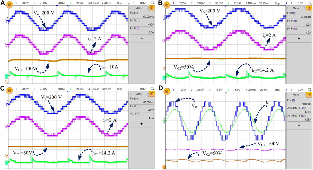
FIGURE 2. Steady-state operating condition. (A) Experimental results of output voltage, load current, voltage across capacitors C1, and capacitor current ic1 at R = 100 Ω. (B) Experimental results of the output voltage, load current, voltage across capacitors C2, and capacitor current ic2 at R = 100 Ω. (C) Experimental results of output voltage, load current, voltage across capacitors C3, and capacitor current ic3 at R = 100 Ω. (D) Experimental results of output voltage, load current, voltage across capacitors C1, and C2 at Z2 = 100 + j100 Ω.
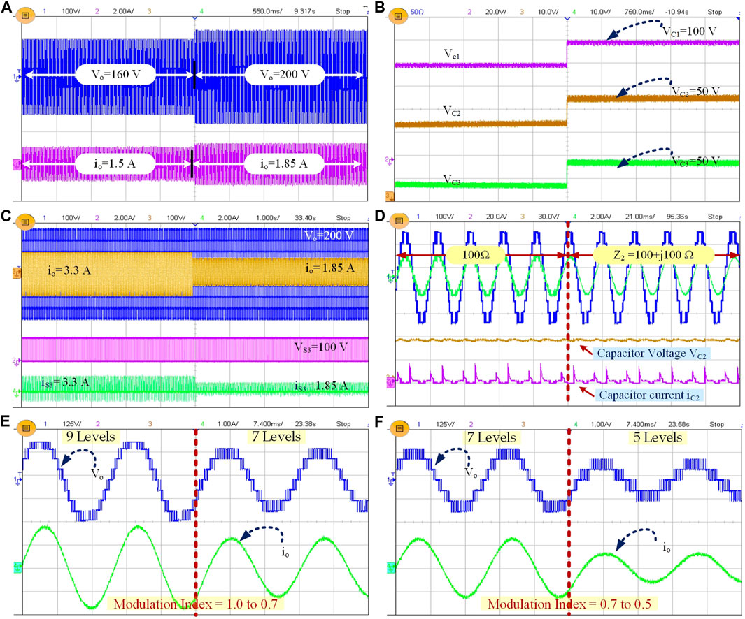
FIGURE 3. Dynamic operating condition. (A) Experimental results of output voltage and load current during step input change. (B) Experimental waveform of capacitor voltages VC1, VC2, and VC3 during step input change. (C) Experimental results of output voltage, load current, voltage, and current of switch S3 during the load change period Z1= 50 + j100 Ω to Z2= 100 + j100 Ω. (D) Experimental results of output voltage, load current, voltage, and current of capacitors C2, during the load change period R = 100 Ω to at Z2 = 100 + j100 Ω. (E) Experimental results of the output voltage and load current during modulation index variations 1.0 to 0.7. (F) Experimental results of the output voltage and load current during modulation index variations 0.7 to 0.5.
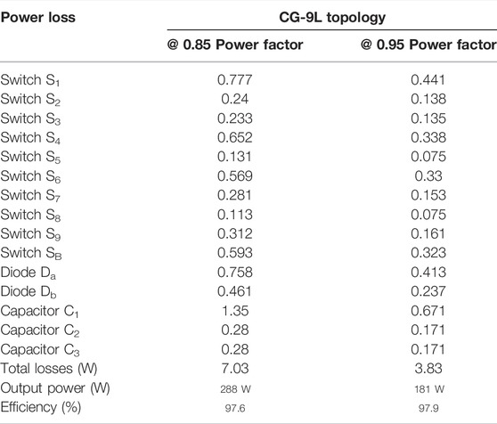
TABLE 1. Power loss and efficiency of the proposed topology.
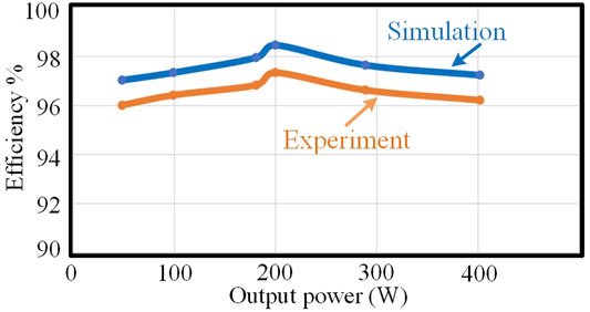
FIGURE 4. Efficiency curve.
The merits of the proposed CG9-L topology in comparison with other recent 9-L topologies are listed in Table 2. The comparison is carried out on the basis of the number of components, Nsh—no. of switches, Ndv—no. of drivers, Nd—no. of diodes, Ncp—no. of capacitors, Tcc—total component count, Tc-L—number of components counts per level, total standing voltage (TSVp.u.), cost function, negative level generation, efficiency, and approximate total cost.
i) The total component utilization ratio of the proposed topology is 2.9, which is less than all remaining topologies except the topologies presented in Iqbal et al. (2021) and Chen et al. (2022). It shows that the CG9-L topology uses minimum power components to produce higher output voltage levels. Despite having a lower component utilization ratio, the voltage stress on some of the switches is high, which is equal to four times the input voltage in topologies (Iqbal et al., 2021; Chen et al., 2022). The total component utilization ratio is calculated as follows:
ii) Even though the topologies presented in Taghvaie and Adabi (2018) and Mohamed Ali et al. (2021) have a lower total standing voltage per unit, it employs more power components than the proposed topology, which increases the total power losses and reduces its efficiency.
iii) Next, the ratio of the total capacitor voltage to the maximum output voltage
iv) Furthermore, the cost function (Cf) is formulated as follows.
and compared with all other topologies. The cost function is calculated with weight factors α = 0.5, 1, and 1.5, and the respective values are listed in Table 2. The cost function of the proposed topology is slightly higher than the topologies presented in (Iqbal et al., 2021; Chen et al., 2022) and less than all other topologies.
v) The approximate cost of the topologies in USD has been calculated and is listed in Table 3. To ensure a fair comparison, all topologies were considered with the goal of producing an output voltage of 400 V, and component ratings were chosen as shown in Table 3. From Table 3, it is clear that the cost of the proposed topology is the least, except for the topology presented in Iqbal et al. (2021).
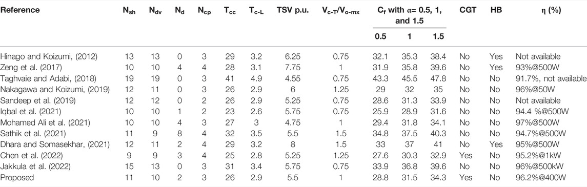
TABLE 2. Comparison with other recent 9L topologies.
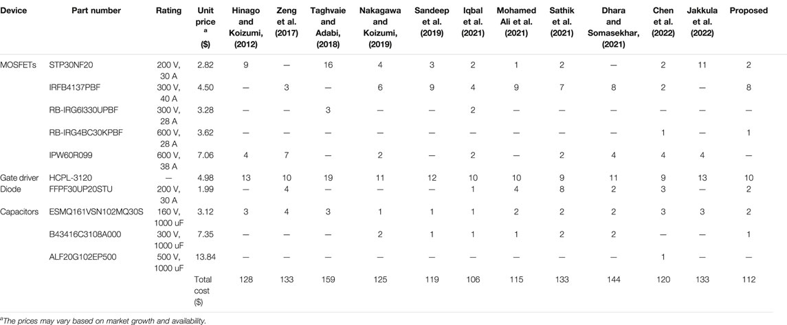
TABLE 3. Cost comparison of the proposed topology with other recent topologies.
The main advantage of the proposed topology is the suppression of leakage current due to its direct connection between the negative terminal of the source side and the neutral of the load side. This common ground connection feature is absent in all other structures except (Chen et al., 2022) listed in Table 2.
This study presented a nine-level inverter with leakage current suppression, voltage boosting, self-voltage balancing, and low voltage stress on capacitors based on a single-phase switching capacitor. The CG feature suppresses the leakage current, making the proposed topology suitable for the transformerless application. The functioning of the proposed topology and capacitance calculation has been discussed. A comprehensive comparison based on power components and capacitor voltage highlights the advantages of the recommended design over the other nine-level topologies. In addition, a complete cost examination confirmed the planned topology’s cost efficiency. The modelling and experimental findings showed that the suggested topology may be implemented under various dynamic operating circumstances without affecting the switched capacitors. Simulation yields a maximum efficiency of ∼97.3 % at 400 W, with a measured result of 96.2%. The suggested topology qualifies as a possible contender for grid-connected photovoltaic application due to the advantages discussed throughout this research.
The original contributions presented in the study are included in the article/Supplementary Material; further inquiries can be directed to the corresponding author.
NG: conceived the idea, designed the experiments, and wrote the manuscript. KV: supervision, formal analysis, review and editing, and validation. Both authors read and approved the final manuscript.
The authors declare that the research was conducted in the absence of any commercial or financial relationships that could be construed as a potential conflict of interest.
All claims expressed in this article are solely those of the authors and do not necessarily represent those of their affiliated organizations, or those of the publisher, the editors, and the reviewers. Any product that may be evaluated in this article, or claim that may be made by its manufacturer, is not guaranteed or endorsed by the publisher.
Babaei, E., Farhadi Kangarlu, M., and Sabahi, M. (2014). Extended Multilevel Converters: An Attempt to Reduce the Number of Independent DC Voltage Sources in Cascaded Multilevel Converters. IET Power Electron. 7, 157–166. doi:10.1049/iet-pel.2013.0057
Chen, M., Yang, Y., Loh, P. C., and Blaabjerg, F. (2022). A Single-Source Nine-Level Boost Inverter with a Low Switch Count. IEEE Trans. Ind. Electron. 69, 2644–2658. doi:10.1109/TIE.2021.3065609
Debnath, D., and Chatterjee, K. (2016). Neutral Point Clamped Transformerless Grid Connected Inverter Having Voltage Buck-Boost Capability for Solar Photovoltaic Systems. IET Power Electron. 9, 385–392. doi:10.1049/iet-pel.2014.0873
Dhara, S., and Somasekhar, V. T. (2021). A Nine-Level Transformerless Boost Inverter with Leakage Current Reduction and Fractional Direct Power Transfer Capability for PV Applications. IEEE J. Emerg. Sel. Top. Power Electron., 1-1. doi:10.1109/JESTPE.2021.3074701
Gonzalez, R., Gubia, E., Lopez, J., and Marroyo, L. (2008). Transformerless Single-phase Multilevel-Based Photovoltaic Inverter. IEEE Trans. Ind. Electron. 55, 2694–2702. doi:10.1109/TIE.2008.924015
Grigoletto, F. B., de Vilhena Moura, P. H. M., Chaves, D. B., and Vilaverde, J. D. S. (2021). Step-Up Seven-Level Common-Ground Transformerless Inverter. 14th IEEE International Conference on Industry Applications (INDUSCON), São Paulo, Brazil, 15-18 Aug. 2021, 716–722. doi:10.1109/INDUSCON51756.2021.9529417
Grigoletto, F. B. (2020). Five-Level Transformerless Inverter for Single-phase Solar Photovoltaic Applications. IEEE J. Emerg. Sel. Top. Power Electron. 8, 3411–3422. doi:10.1109/JESTPE.2019.2891937
Gu, Y., Li, W., Zhao, Y., Yang, B., Li, C., and He, X. (2013). Transformerless Inverter with Virtual DC Bus Concept for Cost-Effective Grid-Connected PV Power Systems. IEEE Trans. Power Electron. 28, 793–805. doi:10.1109/TPEL.2012.2203612
Habib Khan, M. N., Siwakoti, Y. P., Scott, M. J., Ul Hasan, S., Shaffer, B., Li, L., et al. (2020). A Common Ground-type Single-phase Dual Mode Five-Level Switched-Capacitor Transformerless Inverter. Conf. Proc. - IEEE Appl. Power Electron. Conf. Expo. - APEC 2020-March, 15-19 March 2020. New Orleans, LA, USA. 436–441. doi:10.1109/APEC39645.2020.9124205
Heribert, S., Christoph, S., and Jurgen, K. (2003). Inverter for Transforming a DC Voltage into an AC Current or an AC Voltage. Eur. Pat. 1, 369–985.
Hinago, Y., and Koizumi, H. (2012). A Switched-Capacitor Inverter Using Series/parallel Conversion with Inductive Load. IEEE Trans. Ind. Electron. 59, 878–887. doi:10.1109/TIE.2011.2158768
Iqbal, A., Siddique, M. D., Reddy, B. P., and Maroti, P. K. (2021). Quadruple Boost Multilevel Inverter (QB-MLI) Topology with Reduced Switch Count. IEEE Trans. Power Electron. 36, 7372–7377. doi:10.1109/TPEL.2020.3044628
Islam, M., and Mekhilef, S. (2015). H6‐type Transformerless Single‐phase Inverter for Grid‐tied Photovoltaic System. IET Power Electron. 8, 636–644. doi:10.1049/iet-pel.2014.0251
Islam, M., Mekhilef, S., and Hasan, M. (2015). Single Phase Transformerless Inverter Topologies for Grid-Tied Photovoltaic System: A Review. Renew. and Sustain. Energy Rev. 45, 69–86. doi:10.1016/j.rser.2015.01.009
Jakkula, S., Jayaram, N., Pulavarthi, S. V. K., Shankar, Y. R., and Rajesh, J. (2022). A Generalized High Gain Multilevel Inverter for Small Scale Solar Photovoltaic Applications. IEEE Access 10, 25175–25189. doi:10.1109/access.2022.3152771
Kadam, A., and Shukla, A. (2017). A Multilevel Transformerless Inverter Employing Ground Connection between PV Negative Terminal and Grid Neutral Point. IEEE Trans. Ind. Electron. 64, 8897–8907. doi:10.1109/TIE.2017.2696460
Khan, M. N. H., Forouzesh, M., Siwakoti, Y. P., Li, L., Kerekes, T., and Blaabjerg, F. (2020). Transformerless Inverter Topologies for Single-phase Photovoltaic Systems: A Comparative Review. IEEE J. Emerg. Sel. Top. Power Electron. 8, 805–835. doi:10.1109/JESTPE.2019.2908672
Kumari, M., Siddique, M. D., Sarwar, A., Tariq, M., Mekhilef, S., and Iqbal, A. (2021a). Recent Trends and Review on Switched‐capacitor ‐based Single‐stage Boost Multilevel Inverter. Int. Trans. Electr. Energ Syst. 31, 1–28. doi:10.1002/2050-7038.12730
Kumari, S., Verma, A. K., N, S., Yaragatti, U. R., and Pota, H. R. (2021b). An Eight‐switch Five‐level Inverter with Zero Leakage Current. IET Power Electron. 14, 590–601. doi:10.1049/pel2.12041
Kumari, S., Verma, A., Sandeep, N., Yaragatti, U., and Pota, H. (2021c). A Five-Level Transformer-Less Inverter with Self-Voltage Balancing and Boosting Ability. IEEE Trans. Ind. Appl. 57, 6237–6245. doi:10.1109/TIA.2021.3116222
Li, W., Gu, Y., Luo, H., Cui, W., He, X., and Xia, C. (2015). Topology Review and Derivation Methodology of Single-phase Transformerless Photovoltaic Inverters for Leakage Current Suppression. IEEE Trans. Ind. Electron. 62, 4537–4551. doi:10.1109/TIE.2015.2399278
Liu, J., Cheng, K. W. E., and Ye, Y. (2014). A Cascaded Multilevel Inverter Based on Switched-Capacitor for High-Frequency AC Power Distribution System. IEEE Trans. Power Electron. 29, 4219–4230. doi:10.1109/TPEL.2013.2291514
Mohamed Ali, J. S., Alishah, R. S., and Krishnasamy, V. (2019). A New Generalized Multilevel Converter Topology with Reduced Voltage on Switches, Power Losses, and Components. IEEE J. Emerg. Sel. Top. Power Electron. 7, 1094–1106. doi:10.1109/JESTPE.2018.2886214
Mohamed Ali, J. S., Hota, A., Sandeep, N., and Almakhles, D. J. (2022). A Single-Stage Common Ground-type Transformerless Five-Level Inverter Topology. IEEE J. Emerg. Sel. Top. Power Electron. 10, 837–845. doi:10.1109/JESTPE.2021.3095125
Mohamed Ali, J. S., Siddique, M. D., Mekhilef, S., Yang, Y., Siwakoti, Y., and Blaabjerg, F. (2021). Experimental Validation of Nine‐level Switched‐capacitor Inverter Topology with High Voltage Gain. Int. J. Circ. Theor. Appl. 49, 2479–2493. doi:10.1002/cta.3004
Nakagawa, Y., Koizumi, H., and Koizumi, H. (2019). A Boost-type Nine-Level Switched Capacitor Inverter. IEEE Trans. Power Electron. 34, 6522–6532. doi:10.1109/TPEL.2018.2876158
Ponnusamy, P., Velliangiri, S., and Ali, J. S. M. (2020). A Hybrid Switched Capacitor Multi-Level Inverter with High Voltage Gain and Self-Voltage Balancing Ability. Electr. Power Components and Syst. 48, 755–768. doi:10.1080/15325008.2020.1821832
Sandeep, N., Ali, J, S, M., Yaragatti, U, R., and Vijayakumar, K. (2019). Switched-Capacitor-Based Quadruple-Boost Nine-Level Inverter. New Jersy, US:IEEE. 7147–7150. doi:10.1109/TPEL.2019.2898225
Sandeep, N., Sathik, M. J., Yaragatti, U. R., Krishnasamy, V., Verma, R, K., and Pota, H, R. (2020). Common-Ground-Type Five-Level Transformerless Inverter Topology with Full DC-Bus Utilization. IEEE Trans. Ind. Appl. 56, 4071–4080. doi:10.1109/TIA.2020.2996152
Sathik, M. J., Almakhles, D. J., Sandeep, N., and Siddique, M. D. (2021). Experimental Validation of New Self-Voltage Balanced 9L-ANPC Inverter for Photovoltaic Applications. Sci. Rep. 11, 1–14. doi:10.1038/s41598-021-84531-z
Shaffer, B., Hassan, H. A., Scott, M. J., Hasan, S. U., Town, G. E., and Siwakoti, Y. (2018). A Common-Ground Single-phase Five-Level Transformerless Boost Inverter for Photovoltaic Applications. Conf. Proc. - IEEE Appl. Power Electron. Conf. Expo. - APEC 2018-March, 4-8 March 2018, San Antonio, Texas, USA. 368–374. doi:10.1109/APEC.2018.8341037
Siddique, M. D., Iqbal, A., Ali, J. S. M., Mekhilef, S., and Almakhles, D. J. (2020). Design and Implementation of a New Unity Gain Nine-Level Active Neutral Point Clamped Multilevel Inverter Topology. IET Power Electron 13, 3155–3162. doi:10.1049/iet-pel.2020.0437
Siddique, M. D., Mekhilef, S., Shah, N. M., Sathik Mohamed Ali, J., Meraj, M., Iqbal, A., et al. (2019). A New Single Phase Single Switched-Capacitor Based Nine-Level Boost Inverter Topology with Reduced Switch Count and Voltage Stress. IEEE Access 7, 174178–174188. doi:10.1109/ACCESS.2019.2957180
Siwakoti, Y. P., Palanisamy, A., Mahajan, A., Liese, S., Long, T., and Blaabjerg, F. (2020). Analysis and Design of a Novel Six-Switch Five-Level Active Boost Neutral Point Clamped Inverter. IEEE Trans. Ind. Electron. 67, 10485–10496. doi:10.1109/TIE.2019.2957712
Sonti, V., Jain, S., and Bhattacharya, S. (2017). Analysis of the Modulation Strategy for the Minimization of the Leakage Current in the PV Grid-Connected Cascaded Multilevel Inverter. IEEE Trans. Power Electron. 32, 1156–1169. doi:10.1109/TPEL.2016.2550206
Taghvaie, A., and Adabi, J. (2018). A Self-Balanced Step-Up Multilevel Inverter Based on Switched-Capacitor Structure. IEEE Transactions on Power Electronics. 33. 199–209. doi:10.1109/TPEL.2017.2669377
Victor, M., Greizer, F., Bremicker, Sven., and Hibler, U. (2008). Method of Converting a Direct Current Voltage Froma Source of Direct Current Voltage, More Specifically Froma Photovoltac Source of Direct Current Voltage. United States. US7411802B2. Available at: https://patents.google.com/patent/US7411802B2/en%0Ahttps://patentimages.storage.googleapis.com/8d/e6/f4/f97b3a2992d433/US7411802.pdf.
Vosoughi, N., Hosseini, S. H., and Sabahi, M. (2020). A New Transformer-Less Five-Level Grid-Tied Inverter for Photovoltaic Applications. IEEE Trans. Energy Convers. 35, 106–118. doi:10.1109/TEC.2019.2940539
Zeng, J., Wu, J., Liu, J., and Guo, H. (2017). A Quasi-Resonant Switched-Capacitor Multilevel Inverter with Self-Voltage Balancing for Single-phase High-Frequency AC Microgrids. IEEE Trans. Ind. Inf. 13, 2669–2679. doi:10.1109/TII.2017.2672733
Keywords: common ground, leakage current, GRID, transformerless, switched capacitor, photo voltaic, multilevel inverter
Citation: Gopinath NP and Vijayakumar K (2022) Common Ground Nine-Level Boost Inverter for Grid-Connected PV Applications. Front. Energy Res. 10:922786. doi: 10.3389/fenrg.2022.922786
Received: 18 April 2022; Accepted: 16 May 2022;
Published: 29 June 2022.
Edited by:
Jagabar Sathik, Prince Sultan University, Saudi ArabiaReviewed by:
Kaustubh Bhatnagar, Aalborg University, DenmarkCopyright © 2022 Gopinath and Vijayakumar. This is an open-access article distributed under the terms of the Creative Commons Attribution License (CC BY). The use, distribution or reproduction in other forums is permitted, provided the original author(s) and the copyright owner(s) are credited and that the original publication in this journal is cited, in accordance with accepted academic practice. No use, distribution or reproduction is permitted which does not comply with these terms.
*Correspondence: Narayanan Pandurangan Gopinath, Z29waW5hdGhlZWUxNEBnbWFpbC5jb20=
Disclaimer: All claims expressed in this article are solely those of the authors and do not necessarily represent those of their affiliated organizations, or those of the publisher, the editors and the reviewers. Any product that may be evaluated in this article or claim that may be made by its manufacturer is not guaranteed or endorsed by the publisher.
Research integrity at Frontiers
Learn more about the work of our research integrity team to safeguard the quality of each article we publish.