 Fan Feng
 Jingyang Fang
 Ujjal Manandhar3
- 1School of Marine Engineering and Technology, Sun Yat-sen University, Zhuhai, China
- 2School of Control Science and Engineering, Shandong University, Jinan, China
- 3School of Electrical and Electronic Engineering, Nanyang Technological University, Singapore
The isolated dual active bridge (DAB)-based two-stage AC-DC-DC converters have been widely applied in grid-connected power electronics systems. However, the impedance interactions between the DAB converter and the AC-DC rectifier can cause instability problems to the two-stage converter systems. The accurate terminal impedance characteristics of the DAB converters are still not clear due to the high frequency ac conversion stage. This makes it difficult to assess the impacts of the DAB circuit parameters on the stability of the two-stage converters. To address these issues, the impedance models of the DAB converters are originally derived in this paper. Based on the developed impedance models, the stability of the DAB-based two-stage AC-DC-DC converters is analyzed. The impacts of the DAB converter circuit parameters on the stability of the two-stage AC-DC-DC converters are comprehensively revealed by the Bode and Nyquist plots. The analysis results offer instructive implications to finetune the design rules of the DAB converters. The conclusions are validated by comprehensive simulation and experimental results.
1 Introduction
In order to connect various DC energy storage sources, such as the batteries and supercapacitors, to the AC utility grids, one of the most common topologies is the two-stage AC-DC-DC converter which consists of an isolated DC-DC conversion stage and an AC-DC stage (Blaabjerg et al., 2004; Wu et al., 2015; Feng et al., 2020). Among the bidirectional DC-DC converter topologies, the dual active bridge (DAB) converter is becoming more and more popular because of its advantages on the high-power density, galvanic isolation, and soft switching (Krismer and Kolar 2009; Roggia et al., 2013; Ye et al., 2017). Figure 1 shows the DAB-based two-stage AC-DC-DC converter. Literature (Wu et al., 2018) proposed the cooperative triple phase shift (CTPS) control is proposed to eliminate the dual-side flow back currents and reduce the current stress of the DAB converter. The CTPS-based DAB converter has a great potential for being used as the interface converter for the energy storage. Therefore, it is also applied in the two-stage AC-DC-DC converter in this paper.
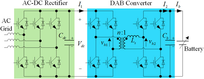
FIGURE 1. Topology of the isolated two-stage AC-DC-DC converter.
However, it is found that this two-stage converter has instability issues. Although the DAB converter and the AC-DC rectifier are stable individually, the instable problem may occur when they are cascaded together. Similar problems have also been reported in other two-stage systems (Radwan and Mohamed 2012; Wu et al., 2012; Liu et al., 2014; Wen et al., 2015). Driven by this issue, a lot of efforts have been made to investigate the stability criterion of the two-stage systems. The concept of the impedance-based stability criterion is first proposed in Literature Middlebrook and Cuk (1976), and later becomes the base for the stability analysis of cascaded systems (Sun 2011; Zhang et al., 2015). A general representation of a two-stage cascaded converter configuration is shown in Figure 2. The stability of the two-stage converter depends on the minor loop gain Tm, expressed as the ratio of the source converter output impedance Zout_S to the load converter input impedance Zin_L. If the impedance ratio Tm satisfies the Nyquist criterion, the two-stage converter will be stable.
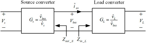
FIGURE 2. Simplified representation of a two-stage converter.
Hence, to analyze the stability of the two-stage converter, it is necessary to derive the impedance models of the AC-DC rectifier and the DAB converter. The impedance model of AC-DC rectifier has been well established. However, the high frequency ac conversion stage brings difficulties to the model generation of the DAB converter. The reduced-order impedance models are derived in Literature (Tian et al., 2016; Tian et al., 2016), based on the “small-ripple” assumption. Since the dc average of the transformer current over a switching period is 0, the dynamics of the transformer current are neglected, thus leading to the sacrifice of accuracy. A full-order discrete-time model, which can obtain higher accuracy compared to the reduced-order model, is developed in Literature Zhao et al. (2010). However, for control design, the continuous model is more desirable. Based on the generalized averaging method, a full-order continuous-time model of the single-phase shift (SPS) modulated DAB converter is proposed and verified to be more accurate than the reduced order models at dc and low frequency (Qin and Kimball 2012). But the model is not extended to the derivation of the DAB converter input or output impedances. In Literature (Mueller and Kimball 2017), the closed-loop impedance of the SPS-DAB converter is calculated based on the Extra Element Theorem with a dummy controller. However, the derivation process is cumbersome and time-consuming for practical use. So far, the existing impedance models are derived from SPS-DAB converters and are not suitable for CTPS-DAB converters. Since the CTPS modulation is drawing increasing attention among the DAB converter applications, the impedance model of the CTPS-based DAB converters should be developed. Moreover, in previous applications, the design of the DAB converter circuit parameters is focused on the steady and dynamic performance (Tan et al., 2012). The influences of the circuit parameters on the stability of the two-stage converter have not been studied yet.
To fill up the gap, the full-order small signal impedance model of the CTPS-based DAB converter is originally derived in this paper. The developed impedance model is used to analyze the stability of the two-stage converter and the influences of the circuit parameters on the stability. Furthermore, the design of the DAB circuit parameters is revisited. The optimization guideline of the DAB circuit parameters is proposed to improve the stability of the two-stage converter.
The rest of this paper is organized as follows. The operation mechanism of the CTPS based DAB converter is analyzed in Section 2. And the small signal impedance models of the two-stage converter are derived in Section 3. The stability of the system and the effects of the filter capacitances are analyzed in Section 4. The simulation and hardware-in-the-loop (HIL) experimental results are presented in Section 5 to verify the theoretical analysis. And Section 6 gives the conclusions of this work.
2 Preliminary: Operation Principle and Stability Assessment of Two-Stage Converters
2.1 Operation Principle of CTPS-DAB Converters
The phase-shift modulation methods are the most widely used to regulate the power transferred in the DAB converters. It has been verified in Literature Wu et al. (2018) that the CTPS modulation can eliminate the dual side flow back currents in the DAB converter and achieve better current characteristics, including the inductor current stress and RMS value. The CTPS-DAB converter is more efficient and reliable compared to other traditional phase-shift control methods. Therefore, the CTPS modulation is applied to the DAB-based two-stage converter in this paper. For the purpose of impedance modeling derivation, the relationship of the three control degrees, i.e., the phase-shift ratios, is given here. The details of the CTPS operation principle is omitted due to space limit but can be found in Literature Wu et al. (2018).
Figure 3 depicts the typical operation waveforms of CTPS-DAB converter. S1–S8 are the driving signals for the switches of the DAB converter. iL is the inductor current. I1 and I2 are the input and output current of the DAB converter, respectively. vh1 and vh2 are the output voltages of the two H-bridges on the primary and secondary side of the transformer, respectively. Ts is the switching cycle of the DAB converter. dφ is the phase-shift ratio between vh1 and vh2. d1 and d2 are the phase-shift ratios of both primary and secondary H-bridges. All the time points t1–t6 can be found in Table 1. The driving signals S4 or S8 is reversed only when the I1 or I2 is zero. Thus, the polarities of vh1 and vh2 can be consistent with that of iL. To meet this requirement, the total increment of iL should be zero during half of a switching cycle, which can be expressed as in Eq. 1. And this constraint can be further simplified as in Eq. 2.
where k = nvdc/vc; vdc is the DC bus voltage; vc is the voltage across the capacitance Cb; n is the turns ratio of the transformer;
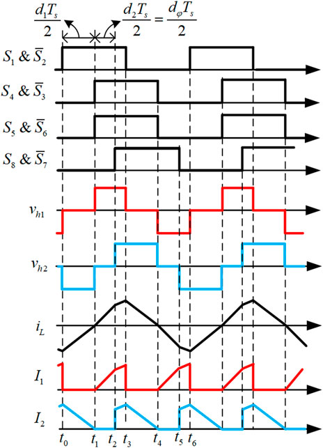
FIGURE 3. Operating waveforms of the CTPS based DAB converter.
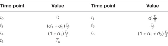
TABLE 1. Mathematical expression of each time point.
The outer phase shift ratio dφ should be equal to d2 to keep the same polarity of vh1 and vh2, namely
2.2 Stability Analysis of Two-Stage Converters
According to Literature Zhang et al. (2015), the stability of the two-stage converter relies on the minor loop gain Tm, which is organized as the ratio of the voltage-controlled converter’s output impedance to the current-controlled converter’s input impedance.
Figure 4 shows the schematic and the control system block diagram of the two-stage AC-DC-DC converter, which is used to connect a battery to the utility grid. Between the DAB converter and the AC-DC rectifier, a DC-bus capacitor Cdc is used to smooth the DC-bus voltage ripple. The control of the two-stage AC-DC-DC converter can be split into two parts: the DC-DC conversion stage and the AC-DC conversion stage. The AC-DC rectifier is responsible for maintaining the DC bus voltage Vdc constant and realizing the grid current closed-loop control. The DAB converter closes the control loop regulating the battery charging current Ib. It should be noted that the control strategy of the two-stage converter keeps the same in bidirectional operation. From Figure 4, Tm can be calculated as:
where Zo_rec is the output impedance of the DC-AC rectifier and Zin_DAB is the input impedance of the DAB converter.
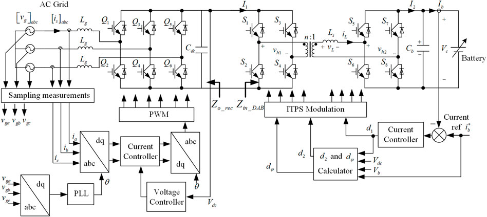
FIGURE 4. The control block diagram of the two-stage AC-DC-DC converter.
The stability analysis of the two-stage converter therefore relies on the model-based determinations of the required impedances in Eq. 4. According to Literature (Tian et al., 2016), two-stage converters have instable problems only when the power is transferred from the voltage-controlled sub-converter to current-controlled sub-converter. Considering the control arrangement in Figure 4, the stability of the two-stage converter in battery charging mode, i.e., the power is transferred from the rectifier to the DAB converter, should be analyzed. Hence, the input impedance of the DAB converter in the battery charging mode are derived in the following section.
2.3 Output Impedance of the AC-DC Rectifiers
The performance and control of the three-phase AC-DC rectifier have been well studied in the existing literature. The derivation process of the small signal model of the rectifier which can be found in Literature Twining and Holmes (2003) is omitted here for conciseness. The output impedance Zo_rec of the rectifier can be expressed as:
where Cdc is the dc-link capacitance; Lg is the input filter inductance of the rectifier; Gci is the controller of the rectifier; ILd is the d-axis component of the inductor current; Dd and Dq denote the d- and q-axes components of the duty ratio of the rectifier, respectively.
3 Impedance Modeling of CTPS-DAB Converters
3.1 Small Signal Impedance Modeling
The impedance model of the CTPS-DAB converter is derived first based on the simplified circuit shown in Figure 5. The voltage-controlled AC-DC rectifier can be regarded as a DC voltage source. Rb is the equivalent load of the battery in the charging operation mode. Rt is the winding resistance of the transformer. The capacitor voltage vc and the inductor current iL are taken as the state variables. The state equations of the CTPS-DAB converter can be expressed as:
where g1 and g2 are the switching functions of the two H-bridges at the primary and secondary sides of the transformer. They can be expressed as follows according to Figure 3.
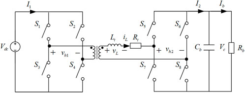
FIGURE 5. The simplified circuit of the DAB converter.
Due to the high-frequency ac link in the DAB converter, the generalized state-space averaging (GSSA) method is applied (Caliskan et al., 1999; Qin and Kimball 2012). The averages of the state variables and the switching functions are approximated by the sum of the index-0 and index-1 coefficient of their Fourier series. This leads to the following state-variable vector,
where the subscripts denote the number of the coefficients of the Fourier series; the superscripts “R” and “I” mean the real and imaginary parts of the first coefficients, respectively. These rules apply in the whole paper.
In Literature Qin and Kimball (2012), the authors show that the dynamics of
Taking the Fourier series of the switching functions, the zeroth coefficients
The resulting GSSA state equations can be obtained as Eq. 15. The output vector
where
The equilibrium point can be derived by solving
The open-loop small signal model of the CTPS-DAB converter is expressed in Eq. 18.
where A, B, C, D are system matrix:
The partial derivatives are given by,
The open-loop transfer functions can be obtained as Eqs 20a–d by solving the open-loop small signal model Eq. 18 using MATLAB.
The battery current is measured in the control loop of the DAB converter. The control block diagram is shown in Figure 6. Gc is the controller of the DAB converter based on PI structure. From Figure 6, the closed-loop input impedance Zin_DAB can be obtained in Eq. 21 based on Mason’s gain formula (Nise 2007).
where T is the loop gain of the DAB converter and
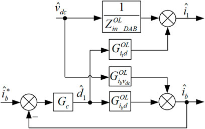
FIGURE 6. Control block of the DAB converter.
And Zin_DAB can be further simplified as Eq. 22.
Eq. 22 can be used to determine the closed-loop input impedance of DAB converters around a certain operating point when the battery voltage changes Vc due to the state-of-charge variations.
It should be mentioned that the battery voltage varies between 270 and 300 V due to the SOC change. Therefore, it is meaningful to investigate the influences of the battery voltage on the DAB input impedance models. Figure 7 shows the bode plots of a set of linearized input impedance models around four different operating points, when Vc is incrementally changed from 270 to 300 V. The magnitude of Zin_DAB is slightly decreased with the increase of Vc, although the phase angles of Zin_DAB are almost the same. According to the Middlebrook criterion, the stability of the two-stage converter requires Zin_DAB larger than Zo_rec. The unstable problem of the two-stage converter most likely happens when the input impedance of the DAB converter presents the lowest magnitude. Therefore, to ensure the stability within the whole operation range, the stability of the two-stage converter should be assessed when the battery voltage is 300 V.
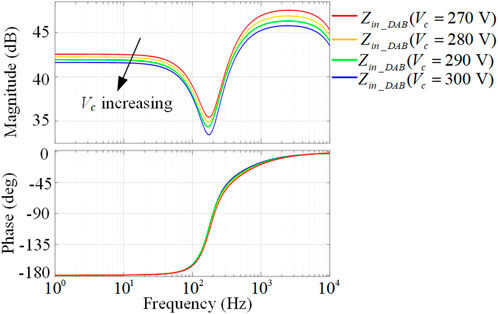
FIGURE 7. Bode plots of Zin_DAB with different Vc.
3.2 Validation of Input Impedance Models
The validity of the developed input impedance model is verified using fully detailed simulation in MATLAB/Simulink environment. The measurement of Zin_DAB is shown in Figure 8. Similar impedance measurement methods have been successfully applied in (Huang et al., 2009; Rygg and Molinas 2017). The parameters of the two-stage converter are shown in Table 2. The deadtime of the switches and the sampling period are set as 0.2 and 250 μs, respectively. The simulation time step is fixed to 0.1 μs. The AC-DC rectifier is replaced by a controllable ripple voltage source connected in series with a 660 V DC voltage source. A sinusoidal perturbation is generated at the DC bus, which is superimposed on steady-state DC voltage as the ripple voltage, vdc_r. The magnitude of vdc_r is set to 1 and the frequency of vdc_r varies logarithmically from 2 Hz to 10 kHz. The corresponding DC bus currents are also measured. The magnitude and phase of the current ripple, idc_r, are extracted by FFT analysis at each frequency. The impedance of the DAB converter at different frequencies can be calculated by Eq. 23.
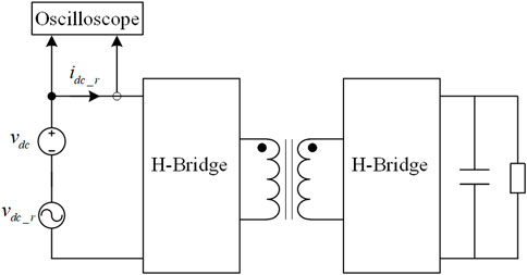
FIGURE 8. Measurement of Zin_DAB.

TABLE 2. Circuit parameters of the two-stage converter.
The bode plots of Zin_DAB with measured values and model predictive values are shown in Figure 9. The impedance model predicted results match well with the measured results from the low frequencies up to the half of the switching frequency fs. Therefore, the developed impedance model can provide fairly accurate prediction for the input impedance of the CTPS-DAB converter. Furthermore, Zin_DAB shows negative resistance characteristics at the low frequencies. Moreover, the magnitude of Zin_DAB is reduced at about 200 Hz. This is the potential threat for stability consideration of the two-stage converter. If the magnitude of Zin_DAB is lower than that of Zo_rec within the low frequency range, the two-stage converter will be unstable. Hence, it is necessary to increase the minimum magnitude value of Zin_DAB. Since the DAB converter circuit parameters are included in the impedance model, the most straightforward method to modify the DAB input impedance is to optimize the DAB circuit parameters. Thus, the effects of the DAB converter circuit parameters on the stability of the two-stage converter should be analyzed.
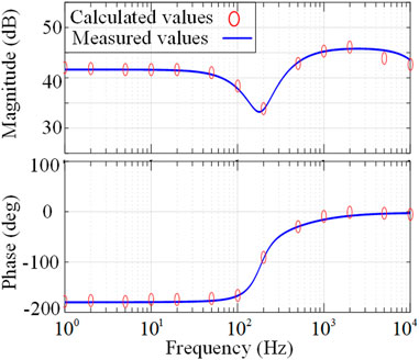
FIGURE 9. Bode plots of the input impedances of the DAB converters. ‘o’ represents the measured values.
4 Stability-Oriented Optimization of Circuit Parameters
For the stability consideration, the magnitude intersection between Zin_DAB and Zo_rec should be avoided. The minimum value of Zin_DAB should be designed in the range above the peak value of Zo_rec. From Eq. 18 to Eq. 22, the inductor Ls and DC side output filter capacitor Cb are included in the impedance model Zin_DAB. Therefore, to improve the stability of the two-stage converter, the most effective and easiest method is to optimize the value of Ls and Cb.
4.1 Stability Improvement by Optimization of Ls
To analyze the effects of Ls on the minimum of Zin_DAB, Figure 10A shows the bode plots of Zin_DAB with different values of Ls. The rest of the circuit parameters are listed in Table 2. The minimum of Zin_DAB increases with the reduction of Ls. When Ls is 200 µH or 100 μH, Zin_DAB intersects with Zo_rec, indicating that the two-stage converter is unstable. However, for Ls smaller than 50 μH, the minimum value of Zin_DAB is larger than the magnitude of Zo_rec within all operation frequencies. According to the Middlebrook criterion, the two-stage converter is stable under such conditions.
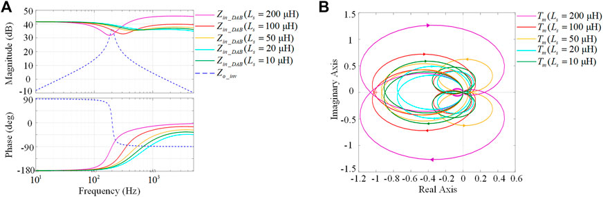
FIGURE 10. (A) Bode plots and (B) Nyquist plots of
The influences of Ls on the stability of two-stage converter can be further illustrated by the Nyquist plots of Tm shown in Figure 10B. The trajectory of Tm encircles the critical point (−1, 0) when Ls is 200 µH or 100 μH, suggesting that there is a right-hand plane pole in the s-plane. The two-stage converter is hence unstable with these two inductors. And the stability of the two-stage converter can be improved by reducing the value of Ls. As seen from Figure 10B, with the reduction of Ls, the gain margin and phase margin are both increased. When Ls is smaller than 50 μH, the trajectory of Tm no longer encircles (−1, 0) anymore. This can also be deduced from Figure 10A, where the minimum value of Zin_DAB is gradually increased with the reduction of Ls. Therefore, for improving the stability of the two-stage converter, a relatively small value of Ls is preferred, although the other factors such as power transfer ability should also be considered.
4.2 Stability Improvement by Optimization of Cb
Similarly, to analyze the influences of Cb on the stability of the two-stage converter, a set of Cb are selected. The relationship between the value of Cb and the minimum magnitude of Zin_DAB is shown in Figure 11A. The minimum magnitude of Zin_DAB keeps decreasing with the reduction of Cb. From Figure 11A, when Cb is larger than 200 μF, Zin_DAB and Zo_rec intersect with each other, which can cause the unstable problem to the two-stage converter.
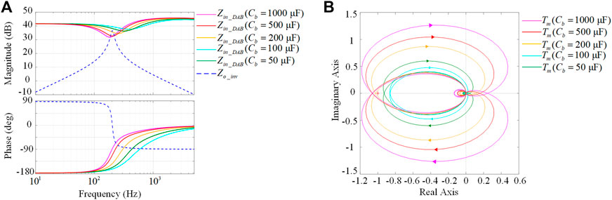
FIGURE 11. (A) Bode plots and (B) Nyquist plots of Tm with decreased Cb.
The effects of Cb on system stability are further illustrated by the Nyquist plots shown in Figure 11B. From Figure 11B, When Cb is larger than 200 μF, the trajectory of Tm encircles the point (−1, 0). This indicates that the two-stage converter cannot maintain its stability. However, with Cb decreasing from 1,000 µF to 50 μF, the gain margin and the phase margin of the two-stage converter increase gradually. And the two-stage converter is stable when Cb is smaller than 100 µF. The conclusion that can be drawn from the Nyquist plot together with the bode plots is that a relatively small value of Cb is good for the stability consideration.
5 Experimental Results and Discussion
The hardware-in-the-loop (HIL) experimental system has been proven to be an effective method for stability analysis of power electronic converters (Zhang et al., 2018). To verify the theoretical analysis, the stability of the two-stage converter is tested based on the OPAL-RT based HIL experimental system. The parameters of the experimental system are shown in Table 2. It should be noted that the waveform of Vdc in Figures 12–15 are only its AC components to show the stability.
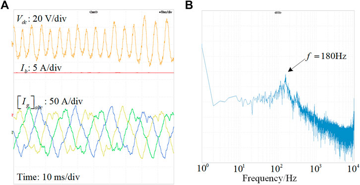
FIGURE 12. (A) Waveforms of the two-stage converter with original parameters; (B) FFT analysis of Vdc with original parameters.
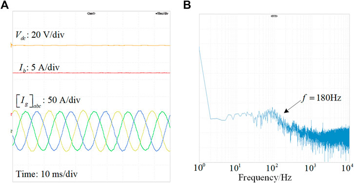
FIGURE 13. (A) Waveforms of the two-stage converter with reduced Ls; (B) FFT analysis of Vdc with reduced Ls.
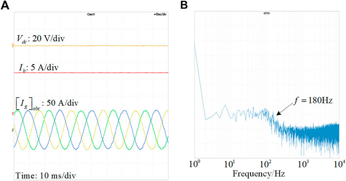
FIGURE 14. (A) Waveforms of the two-stage converter with reduced Cb; (B) FFT analysis of Vdc with reduced Cb.
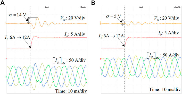
FIGURE 15. (A) Dynamic performance of the two-stage converter with reduced Ls; (B) dynamic performance of the two-stage converter with reduced Cb.
Figure 12A shows the waveforms of the two-stage converter with original circuit parameters (Ls = 200 μH, Cb = 1,000 μF). As seen, the oscillation at Vdc can be found. Moreover, the oscillating frequency is around 180 Hz, which is consistent with the prediction of the bode plot in Figure 10A. The instable problem of the two-stage converter can be more visualized from the FFT spectra of Vdc shown in Figure 12B. The amplitude of the 180 Hz harmonic component is significant. This is the root cause of the waveform oscillation.
Considering the effects of Ls on the minimum magnitude of Zin_DAB, Ls should be reduced to improve the stability. Figure 13A shows the waveforms of the two-stage converter with reduced Ls = 50 µH and other parameters being unchanged. The oscillation at Vdc is mitigated as expected. This is because the minimum magnitude of Zin_DAB is increased and there is no intersection between Zin_DAB and Zo_rec as shown in Figure 10A. It can be also observed from the FFT spectra of Vdc in Figure 13B that the quantities of the 180 Hz harmonic response are suppressed.
Similarly, according to the above-mentioned analysis, Cb should be reduced to for stability consideration. Figure 14A shows the waveforms of the two-stage converter with Cb = 100 µF and other parameters being constant. The waveforms show that the two-stage converter is stable with reduced Cb. According to FFT spectra of Vdc in Figure 14B, the 180 Hz harmonic response is also greatly suppressed.
The dynamic performances of the two-stage converter with reduced Ls and Cb are also tested and shown in Figure 15. When Ib steps up from 6 to 12 A, Vdc can be stabilized with reduced Ls or Cb after a short transient period. However, when reduced Ls is applied, the overshoot of Vdc is about 14 V. When reduced Cb is applied, the overshoot of Vdc is only about 5 V.
Hence, the stability of the two-stage converter can be improved by optimizing Ls or Cb. Furthermore, the dynamic performance of the two-stage converter with reduced Cb is better than that of the two-stage converter with reduced Ls according to the experimental waveforms.
6 Conclusion
The full-order impedance model of the CTPS based DAB converter has been derived in this paper. The developed impedance model can fully represent the dynamics of the ac conversion stage of the DAB converters. Based on the developed impedance model, the stability of two-stage converter has been analyzed. Furthermore, the effects of the DAB circuit parameters on the stability of the two-stage converter have been presented and analyzed. The design of the DAB circuit parameters is revisited. The stability-oriented optimization guideline of circuit parameters is provided for the DAB converter. The stability of the two-stage converter can be improved by reducing the leakage inductance or the DC side output filter capacitance of the DAB converter.
Data Availability Statement
The original contributions presented in the study are included in the article/Supplementary Material, further inquiries can be directed to the corresponding authors.
Author Contributions
FF contributed to the conception of the study and wrote the manuscript; JF performed the data analyses; HG contributed to analysis and manuscript preparation. UM and LW performed the experiment.
Funding
This research was funded by the Special project for marine economy development of Guangdong Province [GDNRC(2022)31], Guangzhou Municipal Science and Technology Bureau (Grant No. 2021020 21161), National Natural Science Foundation of China (Grant No. 52101342), Key-Area Research and Development Program of Guangdong Province (Grant No. 2021B0202070002), and Natural Science Foundation of Guangdong Province (Grant No. 2022A1515010792), Shandong University Distinguished Young Scholars Project grant number 31400012002201.
Conflict of Interest
The authors declare that the research was conducted in the absence of any commercial or financial relationships that could be construed as a potential conflict of interest.
Publisher’s Note
All claims expressed in this article are solely those of the authors and do not necessarily represent those of their affiliated organizations, or those of the publisher, the editors and the reviewers. Any product that may be evaluated in this article, or claim that may be made by its manufacturer, is not guaranteed or endorsed by the publisher.
References
Blaabjerg, F., Chen, Z., and Kjaer, S. B. (2004). Power Electronics as Efficient Interface in Dispersed Power Generation Systems. IEEE Trans. Power Electron. 19 (5), 1184–1194. doi:10.1109/tpel.2004.833453
Caliskan, V. A., Verghese, O. C., and Stankovic, A. M. (1999). Multifrequency Averaging of DC/DC Converters. IEEE Trans. Power Electron. 14 (1), 124–133. doi:10.1109/63.737600
Erika Twining, E., and Holmes, D. G. (2003). Grid Current Regulation of a Three-phase Voltage Source Inverter with an LCL Input Filter. IEEE Trans. Power Electron. 18 (3), 888–895. doi:10.1109/tpel.2003.810838
Feng, F., Zhang, X., Zhang, J., and Gooi, H. B. (2020). Stability Enhancement via Controller Optimization and Impedance Shaping for Dual Active Bridge-Based Energy Storage Systems. IEEE Trans. Industrial Electron. 68 (7), 5863–5874.
Hengsi Qin, H., and Kimball, J. W. (2012). Generalized Average Modeling of Dual Active Bridge DC-DC Converter. IEEE Trans. Power Electron. 27 (4), 2078–2084. doi:10.1109/tpel.2011.2165734
Huang, J., Corzine, K. A., and Belkhayat, M. (2009). Small-signal Impedance Measurement of Power-Electronics-Based AC Power Systems Using Line-To-Line Current Injection. IEEE Trans. Power Electron. 24 (2), 445–455. doi:10.1109/tpel.2008.2007212
Krismer, F., and Kolar, J. W. (2009). Accurate Small-Signal Model for the Digital Control of an Automotive Bidirectional Dual Active Bridge. IEEE Trans. Power Electron. 24 (12), 2756–2768. doi:10.1109/tpel.2009.2027904
Liu, F., Liu, J., Zhang, H., and Xue, D. (2014). Stability Issues of $Z + Z$ Type Cascade System in Hybrid Energy Storage System (HESS). IEEE Trans. Power Electron. 29 (11), 5846–5859. doi:10.1109/tpel.2013.2295259
Middlebrook, R., and Cuk, S. (1976). A General Unified Approach to Modelling Switching-Converter Power Stages. In Power Electronics Specialists Conference. IEEEIEEE. doi:10.1109/pesc.1976.7072895
Mueller, J. A., and Kimball, J. W. (2017). “Model-based Determination of Closed-Loop Input Impedance for Dual Active Bridge Converters,” in Applied Power Electronics Conference and Exposition (APEC), 2017 IEEE (IEEE). doi:10.1109/apec.2017.7930824
Radwan, A. A. A., and Mohamed, Y. A.-R. I. (2012). Assessment and Mitigation of Interaction Dynamics in Hybrid AC/DC Distribution Generation Systems. IEEE Trans. Smart Grid 3 (3), 1382–1393. doi:10.1109/tsg.2012.2201965
Roggia, L., Schuch, L., Baggio, J. E., Rech, C., and Pinheiro, J. R. (2013). Integrated Full-Bridge-Forward DC-DC Converter for a Residential Microgrid Application. IEEE Trans. Power Electron. 28 (4), 1728–1740. doi:10.1109/tpel.2012.2214061
Rygg, A., and Molinas, M. (2017). Apparent Impedance Analysis: A Small-Signal Method for Stability Analysis of Power Electronic-Based Systems. IEEE J. Emerg. Sel. Top. Power Electron. 5 (4), 1474–1486. doi:10.1109/jestpe.2017.2729596
Sun, J. (2011). Impedance-based Stability Criterion for Grid-Connected Inverters. IEEE Trans. Power Electron. 26 (11), 3075–3078. doi:10.1109/tpel.2011.2136439
Tan, N. M. L., Abe, T., and Akagi, H. (2012). Design and Performance of a Bidirectional Isolated DC-DC Converter for a Battery Energy Storage System. IEEE Trans. Power Electron. 27 (3), 1237–1248. doi:10.1109/tpel.2011.2108317
Tian, Y., Loh, P. C., Chen, Z., Deng, F., and Hu, Y. (2016). Impedance Interactions in Bidirectional Cascaded Converter. IET Power Electron. 9 (13), 2482–2491. doi:10.1049/iet-pel.2015.0559
Tian, Y., Loh, P. C., Deng, F., Chen, Z., Sun, X., and Hu, Y. (2016). Impedance Coordinative Control for Cascaded Converter in Bidirectional Application. IEEE Trans. Ind. Appl. 52 (5), 4084–4095. doi:10.1109/tia.2016.2564359
Wen, B., Boroyevich, D., Burgos, R., Mattavelli, P., and Shen, Z. (2015). Small-Signal Stability Analysis of Three-phase AC Systems in the Presence of Constant Power Loads Based on Measured D-Q Frame Impedances. IEEE Trans. Power Electron. 30 (10), 5952–5963. doi:10.1109/tpel.2014.2378731
Wu, F., Feng, F., and Gooi, H. B. (2018). Cooperative Triple-Phase-Shift Control for Isolated DAB DC–DC Converter to Improve Current Characteristics. IEEE Trans. Industrial Electron. 66 (9), 7022–7031.
Wu, F., Li, X., Feng, F., and Gooi, H. B. (2015). Modified Cascaded Multilevel Grid-Connected Inverter to Enhance European Efficiency and Several Extended Topologies. IEEE Trans. Ind. Inf. 11 (6), 1358–1365. doi:10.1109/tii.2015.2486623
Wu, K., de Silva, C. W., and Dunford, W. G. (2012). Stability Analysis of Isolated Bidirectional Dual Active Full-Bridge DC-DC Converter with Triple Phase-Shift Control. IEEE Trans. Power Electron. 27 (4), 2007–2017. doi:10.1109/tpel.2011.2167243
Ye, Q., Mo, R., and Li, H. (2017). Low-frequency Resonance Suppression of a Dual Active Bridge (DAB) DC/DC Converter Enabled DC Microgrid with Constant Power Loads (CPLs) Based on Reduced-Order Impedance Models. IEEE J. Emerg. Sel. Top. Power Electron.
Zhang, X., Ruan, X., and Tse, C. K. (2015). Impedance-based Local Stability Criterion for Dc Distributed Power Systems. IEEE Trans. Circuits Syst. I 62 (3), 916–925. doi:10.1109/tcsi.2014.2373673
Zhang, X., Zhong, Q.-C., Kadirkamanathan, V., He, J., and Huang, J. (2018). Source-side Series-Virtual-Impedance Control to Improve the Cascaded System Stability and the Dynamic Performance of its Source Converter. IEEE Trans. Power Electron.
Keywords: dual active bridge, impedance modeling, stability analysis, two-stage converter, parameter optimization
Citation: Feng F, Fang J, Manandhar U, Gooi HB and Wang L (2022) Impedance Modeling and Stability-Oriented Parameter Optimization of Isolated Dual Active Bridge-Based Two-Stage AC-DC-DC Converter. Front. Energy Res. 10:874467. doi: 10.3389/fenrg.2022.874467
Received: 12 February 2022; Accepted: 10 June 2022;
Published: 30 June 2022.
Edited by:
Sudhakar Babu Thanikanti, Chaitanya Bharathi Institute of Technology, IndiaReviewed by:
Ning Gao, Shanghai Maritime University, ChinaSubhendu Bikash Santra, KIIT University, India
Copyright © 2022 Feng, Fang, Manandhar, Gooi and Wang. This is an open-access article distributed under the terms of the Creative Commons Attribution License (CC BY). The use, distribution or reproduction in other forums is permitted, provided the original author(s) and the copyright owner(s) are credited and that the original publication in this journal is cited, in accordance with accepted academic practice. No use, distribution or reproduction is permitted which does not comply with these terms.
*Correspondence: Jingyang Fang, amluZ3lhbmdmYW5nQHNkdS5lZHUuY24=; Liguo Wang, d2FuZ2xnN0BtYWlsLnN5c3UuZWR1LmNu