 Weikang Wang
 Yang Liu*
- The School of Artificial Intelligence and Automation, Huazhong University of Science and Technology, Wuhan, China
The interleaving technique is required for LLC resonant converters to achieve high power levels, handle higher input/output currents, and reduce output current ripple. However, the high system efficiency and the low output current ripple for the multi-phase LLC resonant converter cannot be achieved at the same time at low and medium power levels. Most methods try to keep the multi-phase LLC resonant converter in load-sharing mode regardless of the power level, which will result in low system efficiency at low and medium power levels. In this paper, an output current ripple and efficiency optimal control method with finite load distribution schemes is proposed for the multi-phase LLC resonant converter to balance the efficiency and output current ripple. The optimal control method improves the efficiency as much as possible while keeping output current ripple low. According to the calculation of output current ripple and efficiency, the optimal load distribution scheme is selected. The pulse-frequency modulation (PFM) and phase-shift modulation (PSM) hybrid control is applied to regulate the load of each phase. An analysis is provided, and a 540-W three-phase interleaved LLC resonant converter is built to verify the superiority.
1 Introduction
Nowadays, with the application and promotion of the third generation wide-bandgap semiconductors such as gallium nitride (GaN) and silicon carbide (SiC), the switching frequency of switching power supplies has risen sharply, promoting the miniaturization and power density of switching power supplies. With advantages of simple structure, zero-voltage switching (ZVS) for MOSFETs, zero-current switching (ZCS) for diodes, low electromagnetic interference (EMI), and high conversion efficiency Li et al. (2020); Park and Jung (2017); Yang et al. (2020); Glitz and Ordonez (2020); Shah et al. (2021); Ta et al. (2020); Menke et al. (2020), LLC resonant converter is suitable for the third generation wide-bandgap semiconductors and widen employed in recent years. However, to achieve ZVS for MOSFETs and ZCS for diodes, LLC resonant converter is operated under the discontinuous-conduction mode (DCM) Liu et al. (2017). In this mode, the ripple of output current is large, which means the capacitance of the output filter capacitor has to be large, and the capacitor faces the reliability challenge. Moreover, the power capacity of the LLC resonant converter is limited. The interleaving technique is usually used on the LLC resonant converter to solve these problems.
Many approaches have been suggested to make multi-phase interleaved LLC resonant converter work together more efficiently and reliably. Researchers mostly prefer the load-sharing method. In Murata and Kurokawa (2016), an interleaved structure of LLC resonant converters without any auxiliary circuit is proposed. The influence of the parameter mismatch is compensated, and the load of each phase is balanced by the effective duty ratio control using PSM. To make the converter suitable for a wide voltage range, the LLC converter in Rehlaender et al. (2020) is operated in full-bridge mode for large gains and in half-bridge mode for low gains. PSM is utilized to balance the output currents during full-bridge mode while asymmetrical duty-cycle mode is proposed for current balancing during half-bridge mode. The converter proposed in Xue et al. (2021) with paralleled half-bridges LLC, the transformers’ secondary sides in reverse series, and shared full bridge rectifier can achieve load sharing by PSM. PSM is utilized in Murata and Kurokawa (2016); Rehlaender et al. (2020); Xue et al. (2021), but the purpose is different. PSM in Murata and Kurokawa (2016) is for balance the output current, while PSM not only regulates the voltage gain but also balances the output current Rehlaender et al. (2020). The PSM control object in Xue et al. (2021) is no longer the different legs in a phase, but two different phases. In Hu et al. (2014b), a switch-controlled capacitor (SCC) is used to control the output voltage by controlling the equivalent resonant capacitance of each LLC stage to balance the output current of each phase, and the converter is operated at a constant switching frequency. In Hu et al. (2014a), a new control strategy with variable switching frequency is proposed for multi-phase LLC resonant converter with SCC. The structure in Sun et al. (2019) using a hybrid rectifier to achieve good load-sharing performance. There are also some passive solutions applied to achieve the same goal. An interleaving LLC resonant converter with a flying capacitor is proposed in Kirshenboim and Peretz (2017). The flying capacitor balances the current distribution between the phases automatically. The common capacitors Wang et al. (2018) or common inductors Wang et al. (2017) are also applied for impedance matching of the phases. Researchers above-mentioned have done much work in the field of multi-phase interleaved LLC resonant converter. They choose the load-sharing method to average the load of each phase. However, the efficiency of LLC resonant converter become low at light load condition, and fully ZVS of MOSFETs is hard to achieve Wen et al. (2020). What is worse, the output voltage cannot be regulated at very light load conditions, although the switching frequency is widely changed Kim et al. (2011). Therefore, if the load-sharing method is applied to multi-phase interleaved LLC resonant converter at light load condition, the system efficiency will be severely affected. Arshadi et al. (2017); Chiba et al. (2020); Arshadi et al. (2021) try to utilize phase shedding to improve the light load performance of three-phase LLC resonant converters. However, because their three-phase structure is not independent, whose three-phase transformer is Y-type connected, their method cannot be directly applied to the multi-phase LLC resonant converter. They turn off one or two phases at light load and turn the converter into a single-phase full-bridge or half-bridge LLC resonant converter to improve the efficiency at light load. Compared with the phase shedding solutions in Arshadi et al. (2017); Chiba et al. (2020); Arshadi et al. (2021), the proposed method comprehensively analyzes the output current ripple and efficiency and selects the optimal distribution scheme according to actual needs, which is more flexible and can achieve multi-objective control. Furthermore, the proposed method can be easily applied to interleaved LLC resonant converters with different phase numbers.
In this paper, a new control method based on optimizing efficiency and output current ripple is proposed. The proposed control method is based on the output current ripple model and system efficiency model, which require output current waveforms and estimated loss model of components. The output current ripple and system efficiency of each load distribution scheme are calculated, and the optimal scheme is selected to apply to the converter. The control method is dedicated to improving efficiency while keeping output current ripple low, especially at low and medium power levels, since the two objectives cannot be both achieved at low and medium power levels. Finally, the proposed control method is applied on a three-phase interleaved LLC resonant converter, and the advantages are verified.
Section 2 discusses the operation principles of the LLC resonant converter and illustrates the output current waveform expression. In Section 3, the estimated loss model of each component is built, and the relationship between output current and efficiency is derived. Section 4 explains the details of the proposed control method. Experimental results are provided in Section 5. Finally, a conclusion is given in Section 6.
2 Output Current Ripple Analysis of LLC Resonant Converter
2.1 Operation Principles and Output Current Ripple Analysis Under PFM Control
The studied multi-phase interleaved LLC resonant converter consists of N parallel converters shown in Figure 1A with only one output filter capacitor Co. The single-phase LLC resonant converter is powered by a DC power supply Vin. The full-bridge circuit consists of switching transistors S1-S4 and freewheeling diodes D1-D4. The resonant tank consists of a resonant inductor Lr, a resonant capacitor Cr, and a magnetizing inductor Lm. The uncontrolled rectifier on the secondary side consists of diodes D5-D8. The output capacitor Co filters the rectified current and outputs it to the load Ro. The converter is operated to regulate the output voltage Vo using PFM.
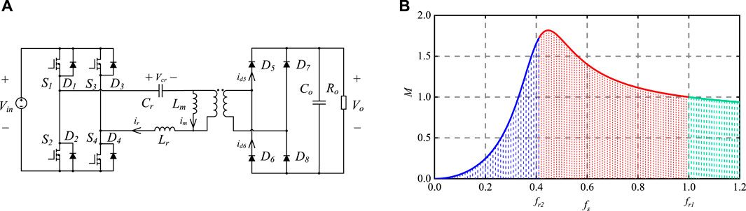
FIGURE 1. (A) Structure of single-phase LLC resonant converter, and (B) input–output voltage gain curve of LLC resonant converter.
Since the ratio of the higher harmonic current of the resonant current to the fundamental harmonic current is very low, the most commonly used analysis method is the fundamental harmonic analysis (FHA) Liu et al. (2017); Sun et al. (2014). Using FHA to analyze the LLC resonant converter, it can be derived that the conversion gain is expressed as follows:
where fr1 and fr2 are the series-resonance frequency and parallel-resonance frequency respectively, Lr is the resonant inductance, Cr is the resonant capacitance, Lm is the magnetizing inductance, ωs is the angular velocity of switching frequency fs, Q is the quality factor of the resonant tank, Req is the resistive load of the resonant network at the FHA model.
Based on Eq. 1, a typical conversion voltage gain M versus switching frequency fs curve is shown as Figure 1B. This conversion gain curve is divided into three regions by fr1 and fr2. To achieve ZVS for MOSFETs and ZCS for diodes, LLC resonant converter is operated in the region fr2 < fs < fr1 Liu et al. (2017). Therefore, the theoretical operating waveforms in this case are analysed with the assumption that the capacitance of the output filter capacitor Co is large enough so that the output voltage Vo remains constant during a switching period.
Theoretical operating waveforms are shown in Figure 2, which are divided into six stages in a switching period. Stages 1–3 are derived from the operation of the switches S1 and S4, while Stages 4–6 are related to the operation of the switches S2 and S3. Stage 1 and Stage 4 show resonance with Lr and Cr. Stage 2 and Stage 5 show resonance with Lm, Lr, and Cr. Stage 3 and Stage 6 represent dead-time durations.
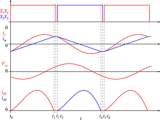
FIGURE 2. Theoretical operating waveforms of LLC resonant converter under PFM control.
Stage 1 [t0 < t < t1]: Since resonant current ir is lower than 0 before t = t0, it flows through diodes D1 and D4, which makes the drain-source voltage Vds of MOSFETs S1 and S4 clamped at − VF1, where VF1 is the forward conduction voltage drop of the freewheeling diode. Therefore, ZVS for MOSFETs S1 and S4 is achieved at t = t0. During this stage, electric power is transferred from the primary side to the secondary side through the transformer. On the secondary side, D5 is forward biased and D6 is reversely biased. The voltage across the transformer secondary side is clamped at the output voltage Vo, so the voltage across the magnetizing inductor Lm remains NVo. Magnetizing current im increases linearly with the slope rate of NVo/Lm. Resonant current ir flows through MOSFETs S1 and S4, fluctuating in sinusoidal form. Therefore, the resonant current ir(t), the resonant capacitors voltage Vcr(t), the magnetizing current im(t), and the secondary current id5(t) can be given as follows:
where I1,ini and V1,ini is the initial value of resonant current ir and resonant capacitor voltage Vcr at t = t0.
Stage 2 [t1 < t < t2]: At t = t1, ir(t) and im(t) become equal, while the energy transmission between the primary side and the secondary side is terminated. Diode current id5 drops to zero in a short time, so ZCS for D5 and D8 is achieved. Magnetizing inductance Lm participates in the resonance between Lr and Cr. Due to Lm is much larger than Lr, resonance angular velocity ωr2 in Stage 2 is much less than ωr1 in Stage 1. Therefore, im and ir are approximately unchanged at this time. The resonant capacitor is charged by the approximately constant current and Vcr rises approximately linearly. Therefore, the resonant current ir(t), the resonant capacitors voltage Vcr(t), the magnetizing current im(t), and the secondary current id5(t) can be derived as follows:
where I2,ini and V2,ini is the initial value of resonant current ir and resonant capacitor voltage Vcr at t = t1. Due to the waveforms of ir, im and Vcr are symmetrical, it can be derived as follows:
where Tr is the resonance period of Lr and Cr (Tr = 1/fr1).
Stage 3 [t2 < t < t3]: At t = t2, MOSFETs S1 and S4 are turned off. The current of resonant tank ir cannot drop to zero immediately because of the inductance. So D2 and D3 start freewheeling. There is still no energy transmission from the primary side to the secondary side, so ir and im remain equal. The conducting of D2 and D3 making S2 and S3 clamped, ready to be turned on with ZVS.
Stage 4–6 [t3 < t < t6]: During these stages, MOSFETs S1 - S4 respectively perform the opposite operation of Stage 1–3. Resonant current ir, magnetizing current im and resonant capacitor voltage Vcr are equal to those in Stage 1–3, but in opposite directions. Diode current id6 repeats the change during Stage 1–3 of id5.
Through the above analysis about steady-state operating process, it can be seen that during the Stage 4–6, energy transmission only happens in the Stage 1 and Stage 4. The average value of the rectifier output current io in a cycle Ts (Ts = 1/fs) is equal to Ioa, which can be expressed as
when the wanted output current Io of LLC resonant converter is determined. V1,ini in Eq. 4 can be derived based on Eq. 13, which is as follows:
I1,ini and V1,ini are derived based on Eq. 12 and Eq. 13, then the ripple of io under steady state can be derived.
2.2 Operation Principles and Output Current Ripple Analysis Under PFM and PSM Hybrid Control
When phase-shift modulation (PSM) control is applied to LLC resonant converters with PFM control together, output characteristics of LLC resonant converter will be changed. According to FHA, the fundamental components of the Vin is related to the effective duty cycle
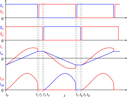
FIGURE 3. Theoretical operating waveforms of LLC resonant converter under PFM and PSM hubrid control.
According to Eq. 1 and Eq. 15, voltage gain ratio using PFM and PSM hybrid control can be modified as
Using Eq. 16, voltage gain of LLC resonant converter can be modified. Meanwhile, PSM have some change on the operation principles and waveforms. The theoretical operating waveforms under PFM and PSM hybrid control can be divided into eight stages in a switching period.
Stage 1 [t0 < t < t1]: Due to the phase shift, S1 has been turned on and S4 is turned on at t = t0. The converter is operated in the same way as Stage 1 under PFM control. Therefore, resonant current ir(t) and magnetizing current im(t) are similar to those under PFM control, which are derived as follows:
where I3,ini is the initial value of resonant current ir, not equal to I1,ini, and V3,ini is the initial value of resonant capacitor voltage Vcr.
Stage 2 [t1 < t < t2]: At t = t1, S1 is turned off. This is the dead-time duration. Due to t1 < Tr/2, energy transmission has not been terminated and ir(t) is larger than im(t), which means the voltage across the transformer secondary side is still clamped at the output voltage Vo. The resonant inductor transfers energy to the power supply and load until im(t) = ir(t). Thus, im(t) remains rises linearly and ir(t) drops quickly. It is a very short period, so it is ignored to simplify the calculation. Assuming ir(t) becomes equal to im(t) as soon as S1 is turned off at t = t1, energy transmission is also terminated.
Stage 3 [t2 < t < t3]: Since in Stage 2, energy transmission has been terminated, and ir(t) becomes equal to im(t). Magnetizing inductance Lm participates in the resonance between Lr and Cr. Magnetizing current im and resonant current ir are approximately unchanged at this time. Meanwhile, id5 becomes zero. Due to the waveforms of ir, im and Vcr are symmetrical, it can be obtained as follows:
where I4,ini and V4,ini is the initial value of resonant current ir and resonant capacitor voltage Vcr at t = t2. Due to the waveforms of ir, im and Vcr are symmetrical, it can be derived as follows:
Stage 4 [t3 < t < t4]: Stage 4 is the dead-time duration. S4 is turned off at t = t3. The operating condition is the same as Stage 2.
Stage 5–8 [t4 < t < t8]: During these stages, MOSFETs S1 - S4 respectively perform the opposite operation of Stage 1–4. Resonant current ir, magnetizing current im and resonant capacitor voltage Vcr are equal to those in Stage 1–4, but in opposite directions. Diode current id6 repeats the change during Stage 1–4 of id5.
Through the above analysis of the operating process under PFM and PSM hybrid control, a conclusion that energy transmission only happens in Stage 1 and Stage 5 can be made by assuming ir(t) drops to im(t) quickly at t = t1 in Stage 2. Thus Eq. 13 still holds and V3,ini can be derived. As long as the waveform of io(t) is determined, the output current ripple can be calculated easily.
3 Estimated Loss Analysis of LLC Resonant Converter
3.1 MOSFETs Loss Analysis and Formula
The loss caused by MOSFETs can be divide into switching loss, on-state loss, and dead-time loss. The switching loss constitutes a significant portion of the power loss in the semiconductor devices Kindl et al. (2015); Hruska et al. (2014); Sojka et al. (2019), which can be further divided into turn-on loss and turn-off loss.
Considering the fact that the on-state resistance Ron of GaN HEMTs is extremely low, only a few tens of milliohms, the on-state loss accounts for a small proportion of MOSFETs loss. The on-state loss WCT of PFM control and hybrid control can be derived as follows:
During dead-time duration, current ir flows through GaN HEMTs’ intrinsic diodes. Unlike silicon MOSFETs, the forward conduction voltage drop of GaN HEMTs’ intrinsic diodes is much larger. Moreover, long-term use of intrinsic diode freewheeling may cause stability risks Sørensen et al. (2015). Therefore, anti-parallel Schottky diodes are often used for GaN HEMTs to reduce primary-side freewheeling diode loss during the dead-time duration. No matter GaN HEMTs’ intrinsic diode or Schottky diodes, the reverse recovery current is zero or very small. The reverse recovery loss can also be ignored. Thus, the dead-time loss is able to be expressed as a freewheeling loss. According to Figure 2 and Figure 3, the dead-time duration of PFM control and hybrid control begins at t2 and t1, respectively. The dead-time loss of two stages is expressed as Eq. 23, where VF1 is the forward conduction voltage drop of the freewheeling diode.
Figure 4 shows the approximated waveforms of the drain-source voltage Vds and current ids under hard switching. The turn-on loss and turn-off loss can be derived as follows:
where td(on) and td(off) are the turning-on delay time and turning-off delay time respectively. Generally, manufacturers and developers provide these parameters.
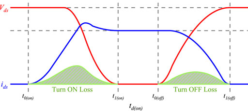
FIGURE 4. Switching loss of MOSFETs under hard switching.
However, according to the analysis of operation principles in Section 2, the current flows through the freewheeling diode before the MOSFET is turned on. The voltage drop on the MOSFET maintains − VF1 during the turning-on delay time. Thus, the turn-on loss under ZVS can be obtained as Eq. 26.
By collecting Eqs 22, 23, 25, 26, the overall power loss for the MOSFETs by multiplying the energies by the switching frequency:
3.2 Parasitic Resistance Loss Analysis and Formula
To make the efficiency model more accurate, the influence of parasitic resistance cannot be ignored. For this purpose, ANSYS Q3D Extractor is a proper choice. Using ANSYS Q3D Extractor to analyze the PCB structure, the Q3D model in Figure 5 can be obtained. Based on the Q3D model, the parasitic resistance can be analyzed, especially the one in the resonant tank Rrt and in the rectifier circuit Rrc. Therefore, the loss caused by parasitic resistance can be obtained as Eq. 28.
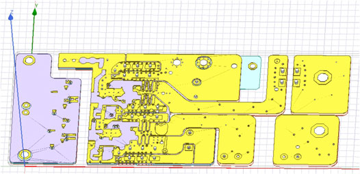
FIGURE 5. Q3D model of the PCB structure.
3.3 Magnetic Component Loss Analysis and Formula
The magnetic components of the LLC resonant converter consist of resonant inductor and transformer. They make up a large part of volume and weight. To improve the power density, sometimes the leakage inductance of transformer is used for resonant inductance and an individual resonant inductor is not needed. Core loss of magnetic components comprises hysteresis and eddy current losses. They are expressed in terms of geometry, material, winding and excitation parameters. The classical core loss can be calculated by
where D is the effective duty cycle. Also, Cm, CT, α, and β are constants provided by the manufacturer.
In addition, the winging losses of the magnetic components are also taken into account. Due to the flowing high-frequency current, the current density in the winding changes, so the impedance becomes larger, and the skin effect cannot be ignored. The skin depth Δ can be obtained as
where μ is the magnetic permeability, and σ is electrical conductance. It is worth mentioning that the parasitic resistance of the wires on the PCB should also consider the skin effect.
3.4 Rectifier Diode Loss Analysis and Formula
In case of high output current, the effect of rectifier diodes becomes significant. Schottky diodes are usually applied in high switching frequency converter for its low forward conduction voltage drop, low reverse current leakage and almost no reverse recovery charge. The reverse recovery time of the Schottky diode is short, and the reverse recovery charge is small. Therefore, the loss of the reverse recovery is very small. In addition, the LLC converter can achieve ZCS on the rectifier diodes, which further reduces the reverse recovery loss of the diodes. Therefore, the reverse recovery loss is ignored and the loss of rectifier diodes is mainly the forward conduction loss. Each rectifier diode works half the time in a cycle and the forward conduction loss of a rectifier diode can be expressed as
where VF2 is the forward conduction voltage drop of the rectifier diode and id is the forward current. Usually, the forward conduction voltage drop VF2 is not a constant, but positively related to forward current id. Hence, the conduction loss can be more accurately expressed as
4 Output Current Ripple and Efficiency Optimal Control Method With Finite Load Distribution Schemes
The system block diagram of the three-phase interleaved LLC resonant converter is shown in Figure 6. To decrease the output current ripple, when the number N of operated phases is more than 1, the phase difference between each phase is
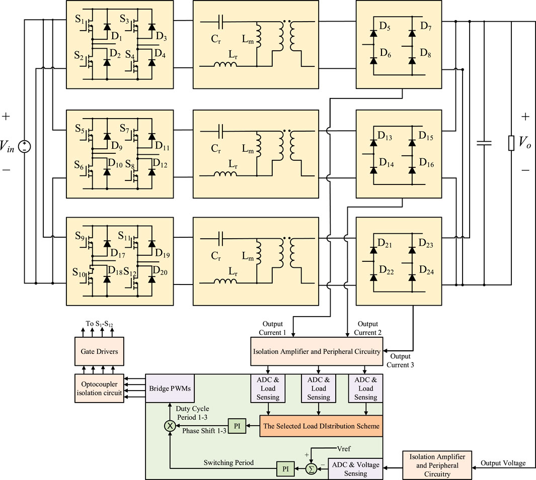
FIGURE 6. Three-phase interleaved LLC resonant converter with a feedback controller.
PFM control is widely applied in LLC resonant converter to regulate the output voltage. According to Eq. 1, in the operation region, the longer the switching period Ts is, the larger voltage gain is. To ensure that the phase difference is stable between the phases in each control cycle, the switching period Ts of each phase remains the same. PSM control is applied to adjust the characteristics of each phase by regulating the duty ratio Murata and Kurokawa (2016); Rehlaender et al. (2020); Yuen et al. (2018). The adjustment of output gain characteristics eventually brings about the adjustment of each phase load, which provides a theoretical basis for load distribution. In addition, although there may be a parameter mismatch between the different phases in practical, the PSM can compensate for the impact.
In Figure 6, the output voltage Vo and output current of each phase Ion (n = 1, 2, 3) are detected. Vo is scaled-down and measured by the analog-to-digital converter (ADC) of the digital signal processor (DSP). The measured Vo is compared with the reference voltage Vref, and the difference is sent into a single-loop PI controller to regulate the switching period Ts. Because Ion changes at a very high frequency, Ion is filtered into Iofn and transformed into a voltage signal. The three filtered voltage signals are measured by ADC, used for load sensing and distribution. Through a single-loop PI controller, the phase shift for each phase is calculated. With the same switching period and different phase shifts, load distribution can be achieved.
Figure 7 shows the control flowchart of the proposed optimal control method, including the optimal load distribution scheme selection algorithm emphasized with the dotted red rectangle in the figure. The converter starts with a soft start, while PFM and PSM hybrid control is applied to regulate the voltage and balance the load of each phase Murata and Kurokawa (2016). During this period, load sensing is to balance the current of each phase and determine whether the load is stable. After the load has stabilized, DSP begins to calculate the efficiency and output current ripple of nos load distribution schemes (nos is the number of the schemes). For the phase with the heaviest load and the largest output current, the parameters such as the equivalent load, circuit parameters, voltage gain ratio M, etc., are substituted into Eq. 1, and the theoretical switching frequency
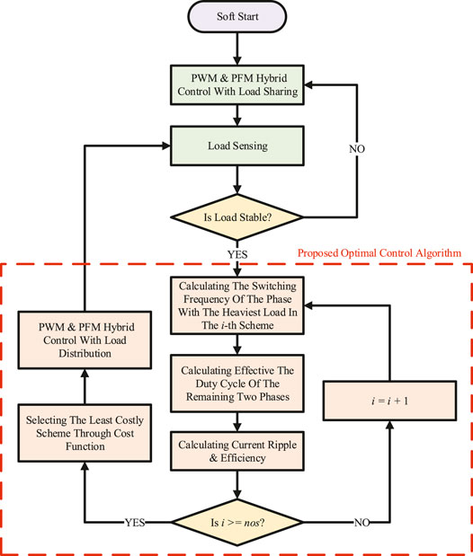
FIGURE 7. The proposed current ripple and efficiency optimal control method.
The cost function is usually expressed as Eq. 33, where λn is the weight coefficient of the n − th term, r* is the effective value of the ripple, and e* is the ratio of power loss to output power Po. The weight coefficient λn determines the focus of the scheme selection. By selecting suitable λn, the preferred control result can be obtained.
It is worth noting that, in order to reduce the amount of calculation, many complex calculations such as output current ripple can be obtained by looking up the table after offline calculation. However, the calculation including the cost function should be performed online, which can better realize the online adjustment of the weight parameters. The output current ripple usually increases as the number N of the operated phases decreases and the equivalent load difference of each phase increases. The output current curves under different load distribution schemes with 120-W output power are obtained by simulation shown as Figure 8. From top to bottom are five load distribution schemes under the same load. Io1, Io2 and Io3 are the output currents of each phase, and Io is the output current of three phases, i.e., Io = Io1 + Io2 + Io3. The first is a three-phase load-sharing scheme. The output current ripple of this scheme is the smallest. The current peak-to-peak value is 11.5% of the average value. The effective value of the current ripple is 3.3% of the average value of the output current, while the effective value of the estimated current ripple accounts for 5.0%. The second is a two-phase load-sharing scheme. The current peak-to-peak value is 28.1% of the average value, and the effective value of the current ripple is 9.2% of the average value, while the effective value of the estimated current ripple accounts for 8.7%. The third scheme is to be operated with 60% load and 40% load respectively for the two phases. The current peak-to-peak value is 102.3% of the average value. The effective value of the current ripple is 32.7% of the average value, while the effective value of the estimated current ripple accounts for 36.8%. The fourth scheme is to be operated with 70% load and 30% load respectively for the two phases. The current peak-to-peak value is 131.9% of the average value. The effective value of the current ripple is 42.4% of the average value, while the effective value of the estimated current ripple accounts for 48.7%. The fifth is a single-phase operation scheme. The current peak-to-peak value is 191.4% of the average value. The effective value of the current ripple is 68.4% of the average value, while the effective value of the estimated current ripple accounts for 62.7%. The time-domain simulation results verify the accuracy of the output current ripple model.
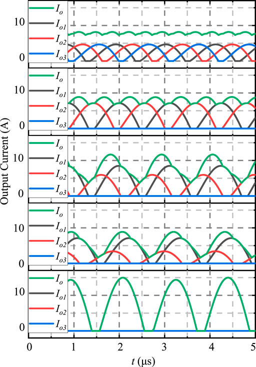
FIGURE 8. The output currents under different load distribution schemes with 120-W output power in simulation.
The system efficiency of single-phase LLC resonant converter usually increases first and then decreases as output power increases, making it possible to achieve efficiency optimization at low and medium power levels. In addition, the higher the accuracy of the efficiency model, the better the efficiency optimization effect will be, but this may result in a larger amount of calculation and a longer calculation time. Further, after calculating the current ripple and output efficiency of a large number of load distribution schemes under various output powers through theoretical models, many load distribution schemes are excluded because they are not practical, and there are few schemes with high practicability. This conclusion is verified by the experiment result. Therefore, excluding impractical load distribution schemes in advance will help reduce the amount of calculation.
5 Experiment Verification
A 540-W three-phase interleaved LLC resonant converter is implemented to verify the feasibility and the advantages of the proposed control method. The converter is shown in Figure 9 and the parameters are shown in Table 1. The full bridge is composed of GaN HEMTs EPC2032 and freewheeling diodes VSS8D5M10. A DSP TMS320F28377D is used to implement the digital controller.
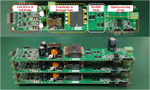
FIGURE 9. The proposed current ripple and efficiency optimal control method.
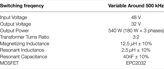
TABLE 1. Converter parameters.
Figure 10 shows the comparison between the estimated efficiency curve based on the analysis in Section 3 and the practical efficiency curves of two different phases of LLC resonant converter. The efficiency curves are measured by ZLG PA5000H power analyzer. It is seen that the matching degree between the estimated curve and the practical curves is high, which can reflect the practical efficiency changes under different loads. When the output power is low than about 60-W, as the output power increases, the system efficiency will increase sharply. At this stage, distributing the load to a certain phase as much as possible can greatly increase the efficiency, but also increase the output current ripple. When the power further increases, especially when the range is greater than about 70-W and lower than about 140-W, the efficiency of the single-phase starts to decline at this stage, while the efficiency of the two-phase is still rising. Therefore, from the perspective of efficiency, the efficiency of two-phase operation is higher. When the power is greater than 170-W, the three-phase load-sharing scheme becomes the optimal one in terms of efficiency and output current ripple. The other load distribution schemes have no advantages in all aspects. Therefore, current ripple and efficiency optimal control method mainly improves the performance of the converter when operated at low and medium power and has little effect on the performance at high power.
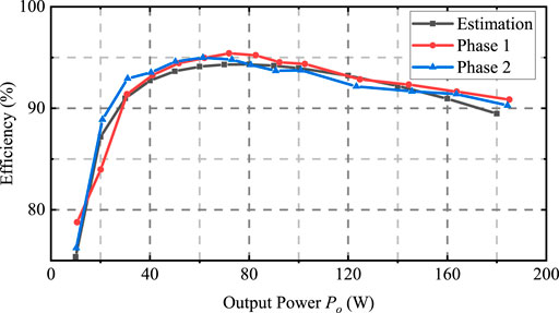
FIGURE 10. Difference between the estimated efficiency curve and the practical efficiency curves.
According to the ripple and efficiency experiments, the effective value of the output current ripple r* of the single-phase mode increases from 0 to 3.5-A as the output power increases, and the efficiency rises rapidly when Po is from 0 to 60-W and slowly decreases when Po is larger than 80 W. Setting λ1 = 0 means that the system will focus on efficiency improvement. In this case, the converter maintains a single-phase mode when the output power is below 110-W, maintains a two-phase current sharing mode in the range from 110 to 190-W, and maintains a three-phase current sharing mode in the range from 190 to 540-W. In order to improve the efficiency at light load and take into account the output current ripple, the experiment chooses λ1 = 2.4 and λ2 = 100. In this case, the converter keeps a single-phase mode below 70-W. In the range from 70 to 160-W, a two-phase current sharing mode is selected. And in the range from 160 to 540-W, a three-phase current sharing mode is selected. At the same time, the steady-state output ripple effective value r* is less than 1-A. However, the cost function is adjusted under the same experimental conditions to show different distribution schemes, and multiple experiments are carried out for comparison.
Figure 11 shows the voltage fluctuations and the current changes of each phase after a step load is applied in three different situations. The voltage in Figure 11 is the converter output voltage measured by ADC, and the current Iofn (n = 1, 2, 3) is the measured value of each phase output current after filtering. In Figure 11A, The first orange dotted line represents the moment when the step load is applied. Vo starts to drop and Io1 increases due to the PI control. At t = 2 ms, the second orange dotted line represents the moment when the system detects the load change and starts to change the load distribution scheme. As described in Section 4, no matter what load distribution scheme the multi-phase LLC resonant converter is operated with, as long as the load changes beyond a certain range, the converter will return to the three-phase load-sharing mode. Therefore, Io2 and Io3 rises rapidly to catch up with Io1. Then, Vo rises to 32.3V until Io is equal to the required load current. The output current stabilizes in 0.95 ms. In Figure 11B, the step load is applied at t = 1.66 ms, highlighted by the first orange dotted line. The system detects the load change at t = 2 ms, and the phase 3 starts working. The system quickly returned to stability in 0.72 ms. In Figure 11C, the step load is applied at t = 1.66 ms. Since the system originally operates in the three-phase load-sharing mode, the load distribution scheme does not change. The system returns to stability in 0.76 ms by PI control. The experimental results show that the controller can capture the load change in a short time (less than 0.5 ms) and make the converter response.
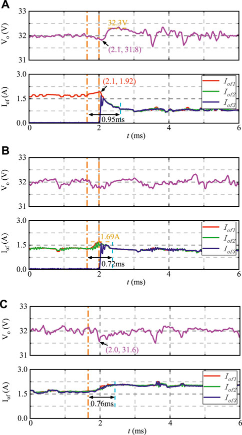
FIGURE 11. Experimental waveforms of the step load response: (A) from 60 to 90-W step load change with single-phase scheme, (B) from 90 to 130-W step load change with two-phase load-sharing scheme, and (C) from 180 to 220-W step load change with three-phase load-sharing scheme.
Figure 12 shows the process of voltage fluctuation and current variation caused by load distribution scheme switching when the output power is 50-W. Firstly, the converter is operated in three-phase load-sharing mode. Then, the load distribution scheme switches at t = 4 ms. Phase 2 and phase 3 are shedding and Io1 starts to rise due to the drop of Vo. Vo drops to 31.59V at t = 0.87 ms and finally stabilizes in 0.87 ms. The efficiency after the scheme switch is improved significantly from 83.1% to 94.5% although the output current ripple of Io become larger. The ratio of the effective value of the ripple to the average value of output current changes from 9.37% to 58.90%. At this power level, single-phase mode is preferred.

FIGURE 12. Experimental waveforms of the load distribution scheme switching at 50-W.
Figure 13A–C show the process of voltage fluctuation and current variation caused by load distribution scheme switching when the output power is 70-W. In Figure 13A, the final load distribution scheme becomes a two-phase load-sharing scheme. In Figure 13B, one phase outputs 60% of the power, and the other phase outputs 40%. In Figure 13C, the converter starts with a three-phase load-sharing mode and switches to a single-phase mode. The output current ripple of these three load distribution schemes increases in turn. The three load distribution schemes change the efficiency from 86.1% to 93.4%, 93.6%, and 95.2%, respectively. Meanwhile, the ratio of the effective value of the ripple to the average value of output current changes from 10.12% to 20.09%, 35.61%, and 57.76%, respectively. At this power level, the efficiency of the single-phase mode is a little higher than that of the two-phase mode but still much higher than that of the three-phase mode. As the output power continues to increase, the single-phase mode will be overall inferior to the two-phase mode, which is in line with the theoretical analysis.
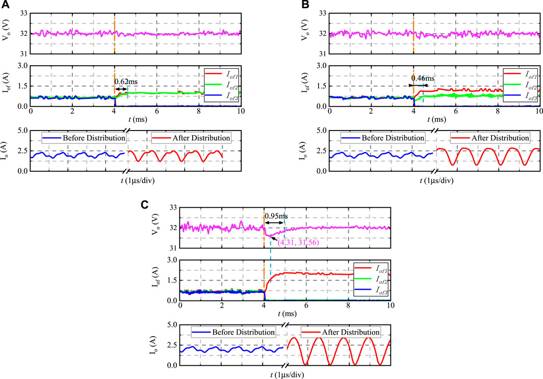
FIGURE 13. Experimental waveforms of the load distribution scheme switching at 70-W: (A) each of the two phases outputing 50% of the power, (B) one phase outputing 60% of the power, and the other phase outputing 40%, and (C) one phase outputing 100% of the power.
Figure 14A and Figure 14B show the process of voltage fluctuation and current variation caused by load distribution scheme switching when the output power is 200-W. At this power level, single-phase mode is excluded and The efficiency of the three-phase mode begins to exceed the efficiency of the two-phase mode. In Figure 14A, the final load distribution scheme becomes a two-phase load-sharing scheme. In Figure 14B, one phase outputs 60% of the power, and the other phase outputs 40%. The two load distribution schemes change the efficiency from 95.1% to 93.9%, and 93.1%, respectively. The ratio of the effective value of the ripple to the average value of output current changes from 11.40% to 18.55%, and 24.09%, respectively. If the output power is further increased, the three-phase load-sharing scheme will undoubtedly become the optimal scheme, and other schemes are ignored.
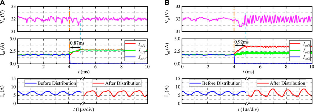
FIGURE 14. Experimental waveforms of the load distribution scheme switching at 70-W: (A) each of the two phases outputing 50% of the power, (B) one phase outputing 60% of the power, and the other phase outputing 40%.
6 Conclusion
The load-sharing control method for the multi-phase interleaved LLC resonant converter leads to a decrease in system efficiency and even affects the normal operation of the converter under light load conditions. In this paper, an output current ripple and efficiency optimal control method for multi-phase interleaved LLC resonant converter is proposed. This optimal control method can adjust the load distribution according to the practical operating conditions of the converter to optimize the current ripple and efficiency. Although the high efficiency and low output current ripple cannot be achieved at the same time in light load, the optimal control method has obvious improvement in efficiency under medium and low load conditions while keeping a low output current ripple. The optimal control method is verified with the 540-W three-phase interleaved LLC resonant converter operated at the 500-kHz switching frequency. Further, the optimal control method can be applied in two-phase converter or multi-phase interleaved LLC resonant converter.
Data Availability Statement
The original contributions presented in the study are included in the article/Supplementary Material, further inquiries can be directed to the corresponding author.
Author Contributions
All authors listed have made a substantial, direct and intellectual contribution to the work, and approved it for publication.
Funding
This work was supported by National Science Foundation of China (NSFC) under Grant 62073147.
Conflict of Interest
The authors declare that the research was conducted in the absence of any commercial or financial relationships that could be construed as a potential conflict of interest.
Publisher’s Note
All claims expressed in this article are solely those of the authors and do not necessarily represent those of their affiliated organizations, or those of the publisher, the editors and the reviewers. Any product that may be evaluated in this article, or claim that may be made by its manufacturer, is not guaranteed or endorsed by the publisher.
References
Arshadi, S. A., Ordonez, M., Eberle, W., Craciun, M., and Botting, C. (2021). Three-Phase LLC Battery Charger: Wide Regulation and Improved Light-Load Operation. IEEE Trans. Power Electron. 36, 1519–1531. doi:10.1109/TPEL.2020.3006422
Arshadi, S. A., Ordonez, M., Mohammadi, M., and Eberle, W. (2017). “Efficiency Improvement of Three-phase LLC Resonant Converter Using Phase Shedding,” in 2017 IEEE Energy Conversion Congress and Exposition, ECCE 2017, 2017-January, 3771–3775. doi:10.1109/ECCE.2017.8096666
Chiba, A., Aoyagi, Y., and Takagi, K. (2020). “Current Balancing and Phase Shedding by Split Capacitor for a Three-phase LLC Resonant Converter,” in ECCE 2020 - IEEE Energy Conversion Congress and Exposition, 377–384. doi:10.1109/ECCE44975.2020.9235978
Glitz, E. S., Hsu, J.-D., and Ordonez, M. (2020). Power Loss Estimation in LLC Synchronous Rectification Using Rectifier Current Equations. IEEE Trans. Ind. Electron. 67, 3696–3704. doi:10.1109/tie.2019.2917372
Hruska, K., Kindl, V., Pechanek, R., and Skala, B. (2014). “Determination of Critical Thermal Operation for Small Squirrel Cage Motor,” in IECON Proceedings (Industrial Electronics Conference), 502–507. doi:10.1109/IECON.2014.7048547
Hu, Z., Qiu, Y., Liu, Y.-F., and Sen, P. C. (2014a). A Control Strategy and Design Method for Interleaved LLC Converters Operating at Variable Switching Frequency. IEEE Trans. Power Electron. 29, 4426–4437. doi:10.1109/TPEL.2014.2300165
Hu, Z., Qiu, Y., Wang, L., and Liu, Y.-F. (2014b). An Interleaved LLC Resonant Converter Operating at Constant Switching Frequency. IEEE Trans. Power Electron. 29, 2931–2943. doi:10.1109/TPEL.2013.2273939
Kim, J.-H., Kim, C.-E., Kim, J.-K., and Moon, G.-W. (2011). “Analysis for LLC Resonant Converter Considering Parasitic Components at Very Light Load Condition,” in 8th International Conference on Power Electronics - ECCE Asia: ”Green World with Power Electronics”, ICPE 2011-ECCE Asia, 1863–1868. doi:10.1109/ICPE.2011.5944387
Kindl, V., Kavalir, T., and Pechanek, R. (2015). “Key Construction Aspects of Low Frequency Wireless Power Transfer System Using Parallel Resonance,” in 2015 17th European Conference on Power Electronics and Applications, EPE-ECCE Europe 2015. doi:10.1109/EPE.2015.7311758
Kirshenboim, O., and Peretz, M. M. (2017). “Two-phase LLC Converter Using a Flying Capacitor for High Output Current Applications,” in 2017 IEEE 18th Workshop on Control and Modeling for Power Electronics, COMPEL 2017. doi:10.1109/COMPEL.2017.8013292
Li, Z., Xue, B., and Wang, H. (2020). An Interleaved Secondary-Side Modulated LLC Resonant Converter for Wide Output Range Applications. IEEE Trans. Ind. Electron. 67, 1124–1135. doi:10.1109/TIE.2019.2897507
Liu, J., Zhang, J., Zheng, T. Q., and Yang, J. (2017). A Modified Gain Model and the Corresponding Design Method for an LLC Resonant Converter. IEEE Trans. Power Electron. 32, 6716–6727. doi:10.1109/TPEL.2016.2623418
Menke, M. F., Duranti, J. P., Roggia, L., Bisogno, F. E., Tambara, R. V., and Seidel, A. R. (2020). Analysis and Design of the LLC LED Driver Based on State-Space Representation Direct Time-Domain Solution. IEEE Trans. Power Electron. 35, 12686–12701. doi:10.1109/TPEL.2020.2995942
Murata, K., and Kurokawa, F. (2016). An Interleaved PFM LLC Resonant Converter with Phase-Shift Compensation. IEEE Trans. Power Electron. 31, 2264–2272. doi:10.1109/TPEL.2015.2427735
Park, H.-P., and Jung, J.-H. (2017). PWM and PFM Hybrid Control Method for LLC Resonant Converters in High Switching Frequency Operation. IEEE Trans. Ind. Electron. 64, 253–263. doi:10.1109/TIE.2016.2599138
Rehlaender, P., Tikhonov, S., Schafmeister, F., and Bocker, J. (2020). “Dual Interleaved 3.6 kW LLC Converter Operating in Half-Bridge, Full-Bridge and Phase-Shift Mode as a Single-Stage Architecture of an Automotive On-Board DC-DC Converter,” in 2020 22nd European Conference on Power Electronics and Applications, EPE 2020 ECCE Europe, 1–10. doi:10.23919/EPE20ECCEEurope43536.2020.9215736
Shah, S. S., Rastogi, S. K., and Bhattacharya, S. (2021). Paralleling of LLC Resonant Converters. IEEE Trans. Power Electron. 36, 6276–6287. doi:10.1109/TPEL.2020.3040621
Sojka, P., Pipiska, M., and Frivaldsky, M. (2019). “GaN Power Transistor Switching Performance in Hard-Switching and Soft-Switching Modes,” in Proceedings of the 2019 20th International Scientific Conference on Electric Power Engineering, EPE 2019. doi:10.1109/EPE.2019.8778060
Sorensen, C., Fogsgaard, M. L., Christiansen, M. N., Graungaard, M. K., Norgaard, J. B., Uhrenfeldt, C., et al. (2015). “Conduction, Reverse Conduction and Switching Characteristics of GaN E-HEMT,” in 2015 IEEE 6th International Symposium on Power Electronics for Distributed Generation Systems, PEDG 2015. doi:10.1109/PEDG.2015.7223051
Sun, J., Tang, X., Xing, Y., Chen, B., Wu, H., and Sun, K. (2019). “Current Sharing Control of Interleaved LLC Resonant Converter with Hybrid Rectifier,” in Conference Proceedings - IEEE Applied Power Electronics Conference and Exposition - APEC, 2019-March, 2223–2227. doi:10.1109/APEC.2019.8721810
Ta, L. A. D., Dao, N. D., and Lee, D.-C. (2020). High-Efficiency Hybrid LLC Resonant Converter for On-Board Chargers of Plug-In Electric Vehicles. IEEE Trans. Power Electron. 35, 8324–8334. doi:10.1109/TPEL.2020.2968084
Wang, H., Chen, Y., Liu, Y.-F., Afsharian, J., and Yang, Z. (2017). A Passive Current Sharing Method with Common Inductor Multiphase LLC Resonant Converter. IEEE Trans. Power Electron. 32, 6994–7010. doi:10.1109/tpel.2016.2626312
Wang, H., Chen, Y., Qiu, Y., Fang, P., Zhang, Y., Wang, L., et al. (2018). Common Capacitor Multiphase LLC Converter with Passive Current Sharing Ability. IEEE Trans. Power Electron. 33, 370–387. doi:10.1109/tpel.2017.2661066
Wen, H., Jiao, D., and Lai, J.-S. (2020). “Light Load Operation Analysis for MHz GaN Based LLC Resonant Converter,” in 2020 IEEE 9th International Power Electronics and Motion Control Conference, IPEMC 2020 ECCE Asia, 1087–1090. doi:10.1109/IPEMC-ECCEAsia48364.2020.9368085
Wenjin Sun, W., Hongfei Wu, H., Haibing Hu, H., and Yan Xing, Y. (2014). “Design Considerations and Experimental Evaluation for LLC Resonant Converter with Wide Battery Voltage Range,” in IEEE Transportation Electrification Conference and Expo, ITEC Asia-Pacific 2014 - Conference Proceedings, 1–6. doi:10.1109/ITEC-AP.2014.6940766
Xue, B., Wang, H., Liang, J., Cao, Q., and Li, Z. (2021). Phase-Shift Modulated Interleaved LLC Converter with Ultrawide Output Voltage Range. IEEE Trans. Power Electron. 36, 493–503. doi:10.1109/TPEL.2020.3001126
Yang, Y., Yao, J., Li, H., and Zhao, J. (2020). A Novel Current Sharing Method by Grouping Transformer's Secondary Windings for a Multiphase LLC Resonant Converter. IEEE Trans. Power Electron. 35, 4877–4890. doi:10.1109/TPEL.2019.2944835
Keywords: interleaved, LLC resonant converter, output current ripple, efficiency, PFM and PSM hybrid control, finite load distribution schemes
Citation: Wang W, Liu Y, Zhao J, Yin Q, Lv Q and Zhang P (2022) Output Current Ripple and Efficiency Optimal Control Method for Multi-Phase Interleaved LLC Resonant Converter. Front. Energy Res. 10:870760. doi: 10.3389/fenrg.2022.870760
Received: 07 February 2022; Accepted: 18 May 2022;
Published: 13 June 2022.
Edited by:
Yongheng Yang, Zhejiang University, ChinaReviewed by:
Qi Zhang, Xi’an University of Technology, ChinaTohid Rahimi, Carleton University, Canada
Copyright © 2022 Wang, Liu, Zhao, Yin, Lv and Zhang. This is an open-access article distributed under the terms of the Creative Commons Attribution License (CC BY). The use, distribution or reproduction in other forums is permitted, provided the original author(s) and the copyright owner(s) are credited and that the original publication in this journal is cited, in accordance with accepted academic practice. No use, distribution or reproduction is permitted which does not comply with these terms.
*Correspondence: Yang Liu, eWFuZ2xpdTMwQGh1c3QuZWR1LmNu