 Xiaolin Zheng
 Xiaoxiao Huang
95% of researchers rate our articles as excellent or good
Learn more about the work of our research integrity team to safeguard the quality of each article we publish.
Find out more
ORIGINAL RESEARCH article
Front. Energy Res. , 12 January 2023
Sec. Process and Energy Systems Engineering
Volume 10 - 2022 | https://doi.org/10.3389/fenrg.2022.1124523
This article is part of the Research Topic Advances in Flexibility Exploration and Utilization for Low Carbon Power Systems View all 6 articles
The three-level active neutral-point-clamped (3L-ANPC) inverters have been widely used in medium-voltage high-power electrical drives. The purpose of this paper is to achieve the reliable operation for 3L-ANPC inverters by reliability analysis and optimal switching and control strategies, while the performance of output waveforms of inverters is maintained. This paper starts by analyzing the power loss and the reliability of power semiconductor devices. On this basis, a mathematical model is derived for online condition monitoring of semiconductor devices. Then, the modulation strategies of the passive commutation mode and the active commutation mode are designed for the 3L-ANPC inverter, and the power loss distributions are analyzed among different semiconductor devices accordingly. Finally, three optimized strategies are designed to improve the reliability of the 3L-ANPC inverter under different load conditions based on different commutation modes and the developed reliability model. Both the simulation using MATLAB Simulink as well as PLECS have been conducted to verify the validity of analysis and control for improving reliability of 3L-ANPC inverters in this paper.
Multilevel inverters have been widely used in medium-voltage high-power electrical applications. With multilevel inverters, low rating power devices can be applied to high-voltage and high-power area, and the problem that output voltage is limited by rated voltage of semiconductor devices can be solved (Wang et al., 2017; Zhang et al., 2019; Quan and Li, 2020). At the same time, as the number of levels increases, the electromagnetic interference as well as the harmonic components of output voltage and output current are reduced. Therefore, the innovation of topologies and control strategies of voltage-source multilevel inverters have drawn a lot of interests. A lot of research work have been devoted to several popular multilevel topologies, including neutral-point-clamped (NPC) inverter (Wang et al., 2018), flying capacitor inverter (Wu et al., 2022), cascaded H-bridge inverters (Song and Huang, 2010) and so on.
In the 1980s, Nabae et al. (1981) proposed the three-level neutral-point-clamped (3L-NPC) inverter topology, as shown in Figure 1A. Compared with the two-level inverter topology, each phase leg is connected to the neutral point “O” by two clamping diodes for the 3L-NPC inverter. This enables each phase leg to output the third voltage level through these clamping diodes, and increases the number of voltage levels. In particular, the 3L-NPC inverter can be used for medium-voltage (MV) applications with the rated voltage from 2.3 kV to 6.6kV, such as the MV wind energy conversion and grid-connected inverters for photovoltaic (PV) generation as well as energy storage. Besides, the 3L-NPC inverters can also be employed in high-power motor drives for compressors, fans, propulsion, etc (Gu et al., 2021).
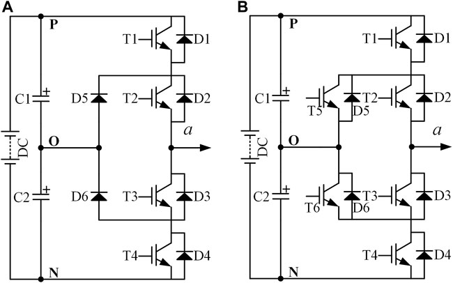
FIGURE 1. Topologies of 3L-NPC inverters. (A) Diode-clamping 3L-NPC inverter. (B) 3L-ANPCinverter.
However, the 3L-NPC inverters have problems in terms of reliability. This topology suffers from the drawback of unequal loss and junction temperature distribution among the semiconductor devices, which limits the increase in switching frequency and capacity of the inverter (Bruckner et al., 2005; Bruckner et al., 2007). In 2001, the topology of the three-level active neutral-point-clamped (3L-ANPC) inverter is proposed, which overcomes the defects of 3L-NPC inverters, as shown in Figure 1B (Bruckner and Bemet, 2001). The clamping diodes connected to the neutral point of 3L-NPC inverters are replaced by the clamping insulated gate bipolar transistors (IGBTs) in the 3L-ANPC inverters. The 3L-ANPC inverter topology increases the switching states and current commutation types. Thus, the junction temperature of semiconductor devices can be balanced to improve the reliability of the system by using different commutation processes (Andler et al., 2014).
Many research works have been performed on control strategies for 3L-ANPC inverters. Jiao and Lee (2015) proposed a new modulation scheme for the 3L-ANPC phase leg. This method takes advantage of the neutral path configuration and balances the loss distribution through a reasonable selection of neutral current paths. Zhang et al. (2016) also proposed a method to balance the conduction loss and the switching loss of semiconductor devices by adopting different control strategies. However, neither of the two methods considers the effect of device junction temperature on loss and lifetime. Bruckner et al. (2005) established an electrothermal model to calculate the junction temperature of the device. It could balance the junction temperature of the 3L-ANPC inverter through different commutation actions and zero states. However, there is no clear classification of different commutation actions, and the evaluation of loss distribution is not sufficient.
To achieve reliable operation for 3L-ANPC inverters, the optimal control strategies of the 3L-ANPC inverter are studied, and an online estimation method is established for reliability and lifetime of 3L-ANPC inverter based on the real time electrical characteristics in this paper. In particular, two different commutation modes are designed for the 3L-ANPC inverter, and the loss distribution of each commutation mode is analyzed accordingly. An electrothermal network as well as a loss prediction model of a 3L-ANPC inverter is developed for the lifetime evaluation. On this basis, the control strategies are proposed to improve the system reliability under different types of loads, while maintaining the output waveform performance of the 3L-ANPC inverter. Simulation has been given to verify the effectiveness of the proposed reliability analysis and reliable operation strategies for 3L-ANPC inverters.
In recent years, power electronics has penetrated into many industrial applications. Due to economic or safety considerations, the system reliability is an issue that cannot be ignored. In the literatures, the studies have been focused on several aspects of reliability for power electronics, including formal reliability assessment, design of fault-tolerant topologies, prognostics and health management approaches, and so on (Hanif et al., 2019). These approaches can evaluate and improve the system reliability in the design stage. However, they are usually proceeded offline and thus cannot prevent the system failure based on the real time conditions. For this reason, this paper aims at proposing an online estimation method for reliability and lifetime of semiconductor devices based on the real time electrical characteristics, and improving the reliability of the 3L-ANPC inverter by using optimal control strategies. At first, the junction temperature calculation process is utilized to evaluate the junction temperature of devices in 3L-ANPC (Zhang et al., 2021).
The relationship between deterioration of semiconductor devices and junction temperature is revealed by the LESIT Study (Held et al., 1997). As expressed in Eq. 1, the number of thermal cycles to failure Nf depends on the thermal swing ΔTj. Tm represents junction temperature in Kelvin, whereas R represents the gas constant, and A, α, and Q are fitting parameters.
On the basis, Miner’s rule can be utilized to calculate the damage effect of semiconductor devices (Raveendran et al., 2019).
where the accumulated damage D can be linearly calculated by the thermal cycles Ni in the ith stress range and the number of thermal cycles to failure Nfi in the ith stress range. When D becomes 1, the device will fail.
The main IGBT losses are conduction losses and switching losses, whereas the main diode losses are conduction losses and turn-off losses (Zhang et al., 2021). Drofenik and Kolar (2005) provided a general scheme for calculating conduction loss, where characteristic parameters can be taken directly from manufactures’ datasheet. Wintrich et al. (2015) provided the formula for switching loss calculation, and the calculation results represents the energy in a switching action. By summing up the conduction loss and the switching loss, the total loss of a power device can be calculated. The calculation methods above are sufficient for estimating the expected power dissipation during converter operation mode in practice.
In general, the thermal characteristics of a system can be described by the thermal equivalent circuits consisting of power sources and thermal impedances (Wintrich et al., 2015), as shown in Figure 2A. Foster network and Cauer network are commonly used as the equivalent thermal circuit, as shown in Figure 2B. In Cauer network, the intermediate points within a block represents system temperatures, while the intermediate points of Foster network do not represent the actual physical location in the system. Thus, this paper uses Cauer network to simulate the thermal impedance. In this way, the junction temperature can be obtained by applying the total losses to the Cauer network. The parameters of the thermal model are obtained from the datasheet of semiconductor devices studied in this paper.
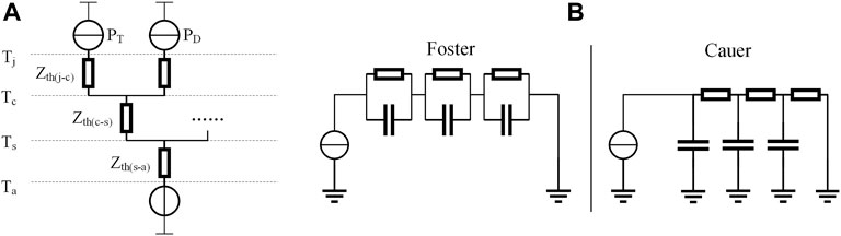
FIGURE 2. (A) Simplified thermal equivalent circuit of IGBT and diode. (B) Two thermal equivalent circuit diagrams.
It should be noted that there are some other methods to measure the junction temperature online besides prediction of junction temperature with thermal model. Actually, the junction temperature of the semiconductor devices can be carried out with some sensitive properties. For example, the on-state Vce of IGBT, the on-state resistance RDS-on of MOSFET and the turn-off delay of devices can be monitored to detect the junction temperature of semiconductor switching devices online (Niu and Lorenz, 2018). These methods are not dependent of the parameters in thermal model, but the additional monitoring hardware are required in the gating drivers or auxiliary detection circuits.
Once junction temperature and thermal swing are known, the lifetime of the device can be estimated by combining Eq. 1, 2. It is possible to calculate the accumulated damage of the device when the power converter is working under a periodic mission profile. However, a random mission profile will generate a random junction temperature profile for the converter, and it is difficult to extract thermal cycles directly. An effective cycle counting algorithm is needed to identify thermal cycles from the load history. The rainflow algorithm can extract thermal cycles from random temperature profile and is widely used for fatigue analysis (Andresen et al., 2018).
The IGBT junction temperature profile in Figure 3A is considered as an example to illustrate the rainflow algorithm. Define the point at which the first derivative from positive to negative as “peak”, and define the point at which the first derivative from negative to positive as “valley”. According to the first three points, X and Y are generated, which represent the algebraic difference between the consecutive peak points and the valley points. The range Y is the algebraic difference between the first and the second points, and the range X is the algebraic difference between the second and the third points. The following are the procedures to determine the thermal cycles according to temperature profile. Set the starting point as S, and start from step 2.
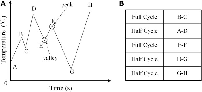
FIGURE 3. Example of the rainflow algorithm. (A) IGBT junction temperature profile. (B) Equivalent thermal cycles according to temperature profile.
Step 1: Find the next peak or valley. If there is no next peak or valley, go to step 5.
Step 2: If there are less than 3 points, go back to step 1. Regenerate X and Y with the 3 latest points that have not been discarded.
Step 3: Compare the absolute values of X and Y. If X < Y, go back to step 1; if X ≥ Y, go to step 4.
Step 4: If Y contains the starting point S, go to step 5. If not, count Y as a full cycle, then discard the peak and the valley contained in Y, and go back to step 2.
Step 5: Count Y as a half cycle, discard the first point in Y, and move the starting point S to the second point in Y. Then, go back to step 2.
Step 6: Define all the ranges that have not been counted as a half cycle.Thus, the results of equivalent thermal cycles are shown in Figure 3B. Based on the equivalent thermal cycles, the device lifetime can be calculated according to Eq. 1, 2.
According to the aforementioned calculation methods of loss, junction temperature and lifetime, an optimal control strategy is presented based on the real-time electrical characteristics. The steps are given as follows.
Step 1: Voltage sensors and current sensors are given to measure the device’s voltage and current. The characteristic curves of devices can be fit from the manufacturer’s datasheet, and power loss can be calculated by the real-time electrical characteristics.
Step 2: Apply the calculated loss to the Cauer network, and the junction temperature of the device can be estimated.
Step 3: The rainflow algorithm is used to extract thermal cycles from the junction temperature profile history. These thermal cycles are used for fatigue analysis, and the device lifetime can be calculated by using lifetime prediction methods.
Step 4: According to the model for online condition monitoring, an optimized control strategy is designed to improve the operation performance and the reliability of the system in real time.
Figure 4 shows the topology of a 3L-ANPC inverter. Each bridge consists of 4 IGBTs in series with antiparallel freewheeling diodes, and the bridge is connected to neutral point O by clamping IGBTs. 3 types of terminal voltage are generated by DC voltage source and DC-link capacitors C1 and C2. The 3L-ANPC inverter has 6 effective switching states, which are given in Table 1.
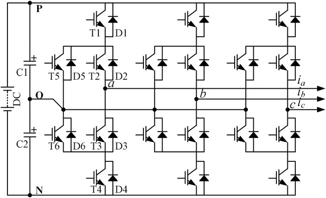
FIGURE 4. Topology of a 3L-ANPC inverter.
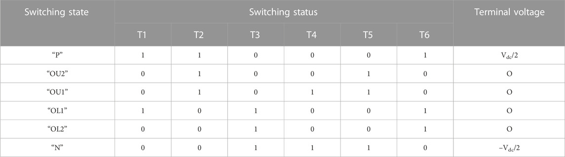
TABLE 1. Switching states of a 3L-ANPC inverter.
There are 16 different commutations in the 3L-ANPC inverter, as shown in Table 2. Zhang et al. (2021) proposed a classification method based on current flow paths to balance loss distribution of power devices. 16 different commutations are divided into passive commutation mode and active commutation mode, while different commutation processes and different loss distributions are reflected directly. Here is a brief introduction of two commutation modes.
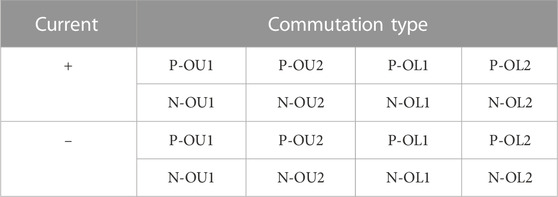
TABLE 2. 16 commutation types in the 3L-ANPC inverter.
Figure 5A shows the loss distribution of passive commutation mode. For 4 quadrants generated by the voltage and current of devices, passive commutation mode is further subdivided into 2 commutation processes of each quadrant. The difference between 2 commutation processes in the same quadrant is switching state “O”. Compared with OU2 and OL2, OU1 and OL1 can prevent turn-off losses caused by antiparallel diodes D1/D4. Therefore, OU1 and OL1 are selected as the optimal states.
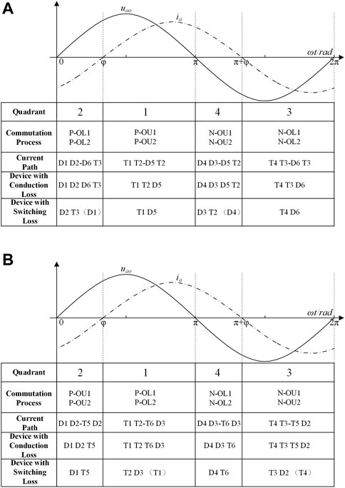
FIGURE 5. Loss distributions. (A) Passive commutation mode. (B) Active commutation mode.
In passive commutation mode, the current paths flow through D5/D6, as shown in the third row of the table in Figure 5A. The power devices that generate losses are shown in the fourth and fifth rows of the table in Figure 5A. By calculating the dwell times in a switching period, the conduction loss of each device within a switching cycle can be calculated accurately. The calculation of switching losses requires the information of the switching state of each device and current flow path in a switching period, then the switching loss of each device in a switching period can be calculated accurately.
Figure 5B shows the loss distribution of active commutation mode. Similarly, active commutation mode is further subdivided into 2 commutation processes of each quadrant Compared with passive commutation mode, current flow path is related to T5/T6 rather than D5/D6, which shows different loss distributions of 2 commutation modes. The power devices that generate losses are shown in the fourth and fifth rows of the table in Figure 5B. The calculation methods of conduction loss and switching loss is the same as that of the passive commutation mode.
Due to different current flow paths in active and passive commutation modes, the loss distribution of 2 commutation modes is completely different. However, an IGBT and a diode will be turned on in any switching state “O”, thus the total loss of passive and active commutation mode is very close. Therefore, it is possible to design control strategies to optimize the loss distribution of devices by using two commutation modes of the 3L-ANPC inverter without affecting system efficiency. Compared to the passive commutation mode, the difference of active commutation mode is to utilized different switching vectors, and the conduction loss and the switching loss will occur in different devices. Consequently, the power loss could be distributed more evenly among different devices in the same inverter leg. The total power loss is almost unchanged by using the active commutation method compared to the passive commutation method.
According to different types of loads, the control strategy of the 3L-ANPC inverter will be different. For constant load, this paper proposes a loss balancing strategy based on comparing loss variance. The implementation of balanced loss distribution is shown in Figure 6A. Combined with the characteristic curves from the manufacturer’s datasheet, the conduction loss and switching loss of each device are estimated by real time voltage and current measurement. On one side, the total loss is applied to Cauer network of the system to calculate the semiconductor junction temperature, and the junction temperature affects the calculation results of total power losses. On the other side, the loss is used to compare two commutation modes of the 3L-ANPC inverter, and the commutation mode with the lower loss variance is selected as the optimal commutation mode. Finally, according to the optimal commutation mode and the reference voltage, the control signal of 18 IGBTs will be generated, which will further determine the switching states of IGBTs in the 3L-ANPC inverter.
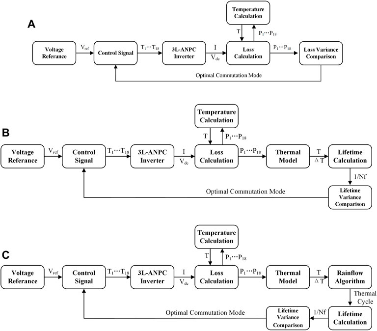
FIGURE 6. Control diagram based on balancing loss and lifetime distribution. (A) Constant load. (B) Periodic load. (C) Random load.
The loss for variance comparison consists of two parts. One part is the cumulative loss, which sums up the conduction loss and the switching loss of each device from the whole load history. The other part is the instantaneous loss, which represents the loss from different commutation modes in the next switching period. However, different commutation modes result in different loss distributions in the same switching period. Therefore, continuously selecting the optimal commutation mode with the lower variance will balance the cumulative loss distribution of all devices.
For periodic loads, this paper proposes a lifetime balancing strategy based on lifetime variance. The implementation of balanced lifetime distribution is shown in Figure 6B. The calculation method of power loss and junction temperature is the same as the control strategy based on loss variance. However, the difference is that the periodic load will produce higher junction temperature fluctuations, so that the lifetime of each device can be calculated. According to the junction temperature and the thermal swing, the remaining lifetime of each IGBT module can be calculated and saved after a load period by combining Eq. 1, 2. The remaining lifetime variance of all IGBT modules is compared under different commutation modes, and the commutation mode with the lower life variance is selected as the optimal commutation mode, which is used to run in the next load cycle. Finally, according to the optimal commutation mode and reference voltage, the control signal of 18 IGBTs will be generated.
The lifetime balancing strategy intuitively demonstrates the system reliability by the lifetime estimation model. The time until the device fails can be calculated, thus device lifetime can be predicted. But for aging devices that have experienced fatigue, the initial damage of devices is still required.
Taking consideration of a more irregular mission profile, the random loads will be tested for the proposed method. For random loads, this paper proposes another lifetime balancing strategy based on lifetime variance, and its control diagram is shown in Figure 6C. The control strategy is similar to the lifetime balancing strategy for periodic load shown in Figure 6B. The difference is that as the load profile is random, and the junction temperature of devices changes irregularly over time. The rainflow algorithm is applied to extract the thermal cycles of devices from the device junction temperature history.
According to the loss balancing strategy based on constant load, a circuit model as well as thermal model of the 3L-ANPC inverter is built on MATLAB Simulink platform. The simulation parameters are shown in Table 3 and the inductive load (R = 4Ω and L = 10 mH) is used as the constant load.
TABLE 3. System parameters.
Figure 7A and Figure 7B shows the distributions of cumulative loss and junction temperature under three different working conditions. It can be seen that the cumulative loss of each power device using the proposed commutation mode is between that using the passive commutation mode and the active commutation mode separately. This is due to the optimal commutation mode can utilize the passive commutation mode and the active commutation mode in an optimal way, which has been as shown in Figure 7C. In Figure 7A and Figure 7B, it also can be observed that the junction temperature distribution and the loss distribution using different commutation modes are consistent, which verifies the analysis in Section 3.
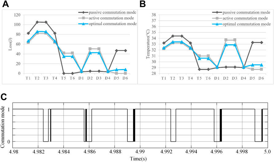
FIGURE 7. Simulation results for constant load (simulated from 0 to 5 s). (A) Cumulative loss distribution. (B) Junction temperature distribution. (C) Selection of optimal commutation mode (0 represents passive commutation mode and 1 represents active commutation mode).
For summarization, Table 4 lists the cumulative loss, the loss variance, the highest junction temperature and the junction temperature variance of different commutation modes. As shown in Table 4, the cumulative losses of different commutation modes remain the same. However, the loss variance and the junction temperature variance of the proposed commutation mode are lower than those of the other two commutation modes. In addition, compared with the other two commutation modes, the highest junction temperature of devices using optimal commutation mode becomes smaller. This indicates that the commutation mode proposed in this paper can facilitate avoiding the premature damage caused by the excessive junction temperature of some devices, so as to prolong the lifetime of the system and improve the system reliability.
TABLE 4. Loss and temperature comparison of different commutation modes.
For periodic loads, this paper proposes a lifetime balancing strategy based on lifetime variance. The simulation parameters are also presented in Table 3. The load shifts between condition R = 9Ω, L = 6 mH and R = 2.25Ω, L = 1.5 mH. The load period TL is 4s. The periodic load is connected to the terminal of the 3L-ANPC. In simulation, we assume that the initial damage of all the devices is zero and the system initially operates in passive commutation mode.
With the aforementioned periodic setting of resistive and inductive load, the power of 3L-ANPC inverter is changed periodically as shown in Figure 8A, where the mission profile changes from 0.2p.u to 0.8p.u. And the power cycle is 4s. The step change from the output power leads to the junction temperature fluctuation of power devices. The accumulated damage of IGBT modules in Figure 8B is calculated from the junction temperature history of power devices. It can be seen from Figure 8B that the accumulated damage will step up after each power cycle, and the selection of the optimal commutation modes is based on the lifetime variance of devices. According to the simulation results from Figure 8C, the optimal commutation mode selected by the strategy is always active commutation mode, rather than commutation modes alternating, except that the system is initially set as passive commutation mode.
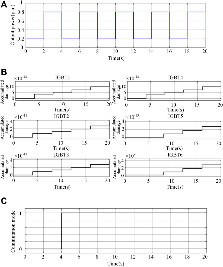
FIGURE 8. Simulation results for periodic load. (A) Mission profile. (B) Accumulated damage of IGBT modules. (C) Selection of optimal commutation mode (0 represents passive commutation mode and 1 represents active commutation mode).
In order to verify the results, further studies are carried out by using the PLECS software, which can combine electrical and thermal quantities in simulation. The simulation parameters remain the same as above. The simulation results are shown in Figure 9 when the system works in the stable operation for 20s, in the passive commutation mode and the active commutation mode respectively. Figure 9 shows the thermal fluctuation ΔT from light load operation to heavy load operation. According to the junction temperature waveforms, the consumed lifetime 1/Nf of devices after a thermal cycle is calculated with Eq. 1 and 2, as shown in Figure 10A and Figure 10B. The data analysis and comparison of different commutation modes are summarized in Figure 10C.
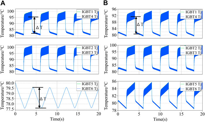
FIGURE 9. Junction temperature of IGBT modules for periodic load. (A) Passive commutation mode. (B) Active commutation mode.
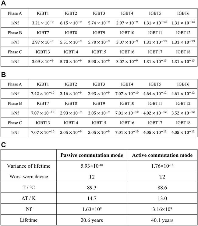
FIGURE 10. (A) Accumulated damage in a load period in passive commutation mode. (B) Accumulated damage in a load period in active commutation mode. (C) Lifetime estimation of different commutation modes.
It can be seen from Figure 10C that the variance of consumed lifetime of active commutation mode is significantly lower than that of passive commutation mode in a load period. The commutation mode with the minimum lifetime variance is continuously selected as the best commutation mode according to the data in Figure 10A and Figure 10B. It is found that no matter how many load periods passed, the consumed lifetime variance of active commutation mode is always with the minimum life variance. In addition, as the most severe worn device in different commutation modes, T2 in passive commutation mode suffers ftrom higher junction temperature and higher junction temperature swing rather than it in active commutation mode. Thus, the system operated in the active commutation mode has longer lifetime, and the active commutation mode is the optimal mode in terms of reliability for the periodic load condition.
The proposed optimal control strategy for reliability is further tested for the random load condition by simulation, and the simulation parameters are also shown in Table 3. The rated load is set as R = 1.8Ω and L = 1.2mH, and the system operates randomly below the rated power. The calculation period of rainflow algorithm is 4s. It is also assumed that the initial damage of all the devices is zero and the system initially operates in passive commutation mode.
Figure 11A shows the irregular mission profile of the inverter system in a time period. The random mission profile generates random junction temperature profile for the converter, and a calculation period is considered to calculate the accumulated damage of devices by using rainflow algorithm and lifetime model. Figure 11B shows the consumed lifetime of all IGBT modules in phase A under random load. It can be seen that the consumed lifetime of IGBT modules steps up after each calculation cycle of rainflow algorithm, and the increment of consumed lifetime is different in each calculation cycle due to the random load profile. Figure 11C shows the commutation mode with the minimum residual lifetime variance. It is found that the optimal commutation mode is always with the active commutation, except that the system initially operates in the passive commutation mode. It can be concluded that the active commutation mode is the optimal mode in terms of reliability for random loads.
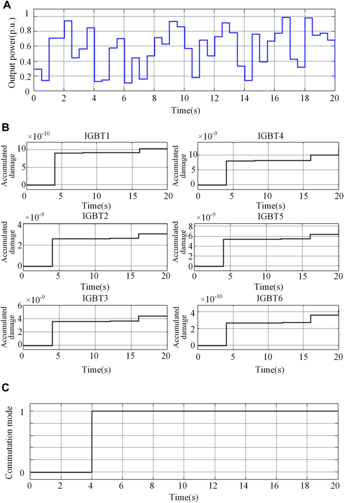
FIGURE 11. Simulation results for random load. (A) Mission profile. (B) Accumulated damage of IGBT modules. (C) Selection of optimal commutation mode (0 represents passive commutation mode and 1 represents active commutation mode).
In this paper, the analysis and optimal control strategies have been presented to achieve the reliable operation for the 3L-ANPC inverter. The conclusions can be drawn as follows.
1. A reliability model has been established for online condition monitoring of the 3L-ANPC inverter, which includes power loss, junction temperature and lifetime calculation of power devices. This reliability model provides the theoretical basis for design of optimal control strategies of reliability for the 3L-ANPC inverter.
2. Two commutation modes, i.e., the active commutation mode and the passive commutation mode have been designed for the 3L-ANPC inverter. The working principle and the power loss distribution have been investigated for the 3L-ANPC inverter. By combining use of the active commutation mode and the passive commutation mode, the power loss can be distributed more evenly among different semiconductor devices.
3. Based on different commutation modes and the reliability model, three optimal strategies have been proposed for improving reliability of the 3L-ANPC inverter under different load conditions. In the case of constant load, the optimal strategy aims at power loss balancing among different devices, while the optimal strategies are developed for the periodic load and the random load based on lifetime estimation.
It should be noted that the ANPC inverter needs two more active switches to clamp the mid-point voltage in DC link compared to the diode-clamping NPC inverter. But ANPC can offer more flexibility in selecting the switching vectors. Both the passive commutation mode and the active commutation mode could be used by ANPC to limit the junction temperatures of difference semiconductor devices. Moreover, more redundant switching vectors can be provided by ANPC inverter than the diode-clamping NPC inverter. Accordingly, higher fault-tolerant capability is owned by ANPC. From both normal operation and faulty operation, the ANPC inverter has higher reliability than the diode-clamping NPC inverter with proper control strategies.
The reliability analysis method is also suitable for monitoring the junction temperatures of semiconductor devices in other power converters. The reliable operation method based on choice of commutation mode is applicable to other power converters with redundant power routes, e.g., multiphase converters and paralleled converters.
The original contributions presented in the study are included in the article/supplementary material, further inquiries can be directed to the corresponding author.
Conceptualization, XZ and XH; methodology, XZ, XH, and PC; simulation validation, ZC and ZY; writing, XZ and XH. All authors have read and agreed to the published version of the manuscript.
This research was funded by State Grid Tianjin Electric Power Company Science and Technology Project with the grant number of KJ22-1–50.
The authors declare that the research was conducted in the absence of any commercial or financial relationships that could be construed as a potential conflict of interest.
All claims expressed in this article are solely those of the authors and do not necessarily represent those of their affiliated organizations, or those of the publisher, the editors and the reviewers. Any product that may be evaluated in this article, or claim that may be made by its manufacturer, is not guaranteed or endorsed by the publisher.
Andler, D., Álvarez, R., Bernet, S., and Rodríguez, J. (2014). Switching loss analysis of 4.5-kV–5.5-kA IGCTs within a 3L-ANPC phase leg prototype. IEEE Trans. Ind. Appl. 50 (1), 584–592. doi:10.1109/TIA.2013.2267331
Andresen, M., Raveendran, V., Buticchi, G., and Liserre, M. (2018). Lifetime-based power routing in parallel converters for smart transformer application. IEEE Trans. Ind. Electron. 65 (2), 1675–1684. doi:10.1109/TIE.2017.2733426
Bruckner, T., and Bemet, S. (2001). Loss balancing in three-level voltage source inverters applying active NPC switches. IEEE 32nd Annu. Power Electron. Spec. Conf. 2, 1135–1140. doi:10.1109/PESC.2001.954272
Bruckner, T., Bernet, S., and Guldner, H. (2005). The active NPC converter and its loss-balancing control. IEEE Trans. Ind. Electron. 52 (3), 855–868. doi:10.1109/TIE.2005.847586
Bruckner, T., Bernet, S., and Steimer, P. K. (2007). Feedforward loss control of three-level active NPC converters. IEEE Trans. Ind. Appl. 43 (6), 1588–1596. doi:10.1109/TIA.2007.908164
Drofenik, U., and Kolar, J. W. (2005). “A general scheme for calculating switching and conduction-losses of power semiconductors in numerical circuit simulations of power electronic systems,” in 5th International Conference on Power Electronics (Niigata, Japan: Institute of Electrical Engineers of Japan), 488–S52.
Gu, M., Wang, Z., Yu, K., Wang, X., and Cheng, M. (2021). Interleaved model predictive control for three-level neutral-point-clamped dual three-phase PMSM drives with low switching frequencies. IEEE Trans. Power Electron 36 (10), 11618–11630. doi:10.1109/TPEL.2021.3068562
Hanif, A., Yu, Y., DeVoto, D., and Khan, F. (2019). A comprehensive review toward the state-of-the-art in failure and lifetime predictions of power electronic devices. IEEE Trans. Power Electron 34 (5), 4729–4746. doi:10.1109/TPEL.2018.2860587
Held, M., Jacob, P., Nicoletti, G., Scacco, P., and Poech, M. -H. (1997). “Fast power cycling test of IGBT modules in traction application,” in Proceedings of Second International Conference on Power Electronics and Drive Systems, Singapore, 26-29 May 1997 (IEEE), 425–430. doi:10.1109/PEDS.1997.618742
Jiao, Y., and Lee, F. C. (2015). New modulation scheme for three-level active neutral-point-clamped converter with loss and stress reduction. IEEE Trans. Ind. Electron. 62 (9), 5468–5479. doi:10.1109/TIE.2015.2405505
Nabae, A., Takahashi, I., and Akagi, H. (1981). A new neutral-point-clamped PWM inverter. IEEE Trans. Ind. Appl. IA-17 (5), 518–523. doi:10.1109/TIA.1981.4503992
Niu, H., and Lorenz, R. D. (2018). Real-time junction temperature sensing for silicon carbide MOSFET with different gate drive topologies and different operating conditions. IEEE Trans. Power Electron. 33 (4), 3424–3440. doi:10.1109/TPEL.2017.2704441
Quan, Z., and Li, Y. (2020). Multilevel voltage-source converter topologies with internal parallel modularity. IEEE Trans. Ind. Appl. 56 (1), 378–389. doi:10.1109/TIA.2019.2941924
Raveendran, V., Andresen, M., and Liserre, M. (2019). Improving onboard converter reliability for more electric aircraft with lifetime-based control. IEEE Trans. Ind. Electron. 66 (7), 5787–5796. doi:10.1109/TIE.2018.2889626
Song, W., and Huang, A. Q. (2010). fault-tolerant design and control strategy for cascaded H-bridge multilevel converter-based STATCOM. IEEE Trans. Ind. Electron. 57 (8), 2700–2708. doi:10.1109/TIE.2009.2036019
Wang, Z., Wang, Y., Chen, J., and Cheng, M. (2017). fault-tolerant control of NPC three-level inverters-fed double-stator-winding PMSM drives based on vector space decomposition. IEEE Trans. Ind. Electron. 64 (11), 8446–8458. doi:10.1109/TIE.2017.2701782
Wang, Z., Wang, Y., Chen, J., and Hu, Y. (2018). Decoupled vector space decomposition based space vector modulation for dual three-phase three-level motor drives. IEEE Trans. Power Electron 33 (12), 10683–10697. doi:10.1109/TPEL.2018.2811391
Wintrich, A., Nicolai, U., Tursky, W., and Reimann, T. (2015). Application manual power semiconductors SEMIKRON. Available at: https://www.semikron-danfoss.com/dl/service-support/downloads/download/semikron-application-manual-power-semiconductors-english-en-2015.pdf.
Wu, M., Tian, H., Wang, K., Konstantinou, G., and Li, Y. (2022). Generalized low switching frequency modulation for neutral-point-clamped and flying-capacitor four-level converters. IEEE Trans. Power Electron 37 (7), 8087–8103. doi:10.1109/TPEL.2022.3147258
Zhang, B., Zou, Z. -X., and Wang, Z. (2021). “Analysis and comparison of three-level ANPC with different commutation modes,” in 2021 IEEE 19th International Power Electronics and Motion Control Conference (PEMC), Gliwice, Poland, 25-29 April 2021 (IEEE), 867–873. doi:10.1109/PEMC48073.2021.9432581
Zhang, D., He, J., and Pan, D. (2019). A megawatt-scale medium-voltage high-efficiency high power density “SiC+Si” hybrid three-level ANPC inverter for aircraft hybrid-electric propulsion systems. IEEE Trans. Ind. Appl. 55 (6), 5971–5980. doi:10.1109/TIA.2019.2933513
Zhang, G., Yang, Y., Iannuzzo, F., Li, K., Blaabjerg, F., and Xu, H. (2016). “Loss distribution analysis of three-level active neutral-point-clamped (3L-ANPC) converter with different PWM strategies,” in 2016 IEEE 2nd Annual Southern Power Electronics Conference (SPEC), Auckland, New Zealand, 05-08 December 2016 (IEEE), 1–6. doi:10.1109/SPEC.2016.7846157
Keywords: three-level active neutral-point-clamped (3L-ANPC) inverter, loss calculation, electrothermal network, reliability, commutation
Citation: Zheng X, Huang X, Chen P, Chong Z and Yuan Z (2023) Reliability analysis and reliable operation of three-level ANPC inverter. Front. Energy Res. 10:1124523. doi: 10.3389/fenrg.2022.1124523
Received: 15 December 2022; Accepted: 28 December 2022;
Published: 12 January 2023.
Edited by:
Yu Liu, Southeast University, ChinaCopyright © 2023 Zheng, Huang, Chen, Chong and Yuan. This is an open-access article distributed under the terms of the Creative Commons Attribution License (CC BY). The use, distribution or reproduction in other forums is permitted, provided the original author(s) and the copyright owner(s) are credited and that the original publication in this journal is cited, in accordance with accepted academic practice. No use, distribution or reproduction is permitted which does not comply with these terms.
*Correspondence: Xiaolin Zheng, Nzg2MTI4MzA4QHFxLmNvbQ==
Disclaimer: All claims expressed in this article are solely those of the authors and do not necessarily represent those of their affiliated organizations, or those of the publisher, the editors and the reviewers. Any product that may be evaluated in this article or claim that may be made by its manufacturer is not guaranteed or endorsed by the publisher.
Research integrity at Frontiers
Learn more about the work of our research integrity team to safeguard the quality of each article we publish.