 Ning Li
 Zhuang Li1
95% of researchers rate our articles as excellent or good
Learn more about the work of our research integrity team to safeguard the quality of each article we publish.
Find out more
ORIGINAL RESEARCH article
Front. Energy Res. , 10 January 2023
Sec. Process and Energy Systems Engineering
Volume 10 - 2022 | https://doi.org/10.3389/fenrg.2022.1087775
This article is part of the Research Topic Planning and Operation of Hybrid Renewable Energy Systems, Volume II View all 12 articles
The Buck circuit is a common topology in DC-DC converter. The existing control strategies have the advantages of short modulation time and high dynamic performance, but they also have the disadvantages of poor active modulation of the working mode of the converter and large current stress. In response to the above problems, an improved frequency/amplitude modulation control strategy is proposed in this paper. The relationship between the output power and the peak inductor current in three modes, namely, Discontinuous Conduction Mode Critical Conduction Mode (CRM) and Continuous Conduction Mode is derived. The precise control strategy of the inductor peak current is introduced based on the traditional voltage loop control strategy to realize the free control of the system working mode and reduce the current stress during the working process. Finally, the experimental platforms of 100V/12V and 220/80V are established respectively. The experimental results show that the flexible switching circuit operating mode in the full load range can be realized under the new control method. In the 100/12V experimental platform, the current stress of the switch tube is optimized by at least 10.7%, and the average system efficiency is improved by 2.21%, with the same main circuit parameters.
DC/DC power conversion is an important research field of power electronics technology, and the Buck circuit is widely used as a step-down converter (Wang et al., 2019a; Chen et al., 2021; Kim et al., 2022a; Liu et al., 2022a; Asad et al., 2022; Talebian et al., 2022; Zhao et al., 2022). With the rapid development of modern information science, how to optimize the performance of the Buck circuit has become a research hot spot in the field of DC/DC power converters.
The circuit control strategy is one of the focuses of current researches, which can be divided into the variable amplitude control and the variable frequency control (Lin et al., 2022; Ripamonti et al., 2019; Liu et al., 2022b; ul Ain et al., 2021). The variable amplitude control is to complete the control target by changing the amplitude of the controlled variable. The variable frequency control modulates the output of the circuit by changing the operating frequency of the switch tube. Both types of control strategies can achieve the goal of regulated output, but they have their own advantages and disadvantages (Nguyen et al., 2019; Hwang et al., 2021; Kim et al., 2022b).
The variable amplitude control strategy controls the output voltage by changing the amplitude of the reference voltage in the single voltage loop, and realizes the control of the system by adding the adjustment of the inductor current amplitude in the voltage and current double closed loop (Nan et al., 2018; Al-Baidhani et al., 2021; Kim and Shin, 2021). The peak current control collects the inductor current as an input signal of the comparator, which feeds back not only the output voltage but also the inductor current to improve the transient response characteristics of the converter (Alexandru and Mircea, 2019; Chen and Lai, 2019). Corresponding to the peak current control, the valley current collects the lowest value of the inductor current as the input signal of the comparator, which is symmetrical with each other in some specific cases (Abdelhamid et al., 2019). The peak current control is more suitable for the case of long conduction time, while the valley current control solves the deficiency that the peak current modulation is not suitable for the short conduction time of the switch tube. Compared with the traditional voltage loop control, the dynamic response speed of the valley current control has been improved, and the control accuracy has also been improved (Wang et al., 2019b), but when the duty cycle is less than 0.5, the valley current control will generate sub-harmonics oscillation. To solve the problem of sub-harmonic oscillation, the average current control (Yang et al., 2018) was proposed. The average current control method has strong anti-noise ability, so it has been widely used. In addition, the current loop is stable over a wide range of input voltages. Several methods were proposed to calculate the average inductor current, using an approach based on average small signal modeling to capture the dynamics of the inner current loop. However, the design of closed-loop parameters in application was more complicated, which increased the complexity of its application. The charge control (Sun et al., 2019) was a special current control, which used the integral value of the inductor current in one cycle as the input of the control loop to control the amount of charge entering the loop in one cycle. Under this control method, the current flowing into the system could be controlled more effectively, with better transient performance and good modulation accuracy, which could meet the high requirements of the power supply. However, its sensitivity to dynamic parameter changes was weak, and harmonic oscillation would occur under light load conditions.
There are also some researches for the variable frequency control at home and abroad. The variable frequency control under the constant on-time is to change the frequency of the control quantity to control the energy transfer under the condition of ensuring a certain conduction time of the switch tube, and finally realize the follow-up of the system expectations. (Calam et al., 2019). realized the modulation of the output voltage under this control method. Compared with the traditional variable amplitude control, the transient performance of the system was improved, but the steady-state accuracy of its control was still insufficient. Compared with the variable frequency control with constant on-time, (Fang and Redl, 2015), proposed a variable frequency control based on a constant off-time. Under the normal working range, for the disturbance of the inductor current, the transient control effect was faster and more stable than the traditional ones, but the steady-state accuracy of the system was still insufficient. Hysteresis control was also a kind of variable frequency control, which changed the frequency of the collected objects by changing the loop width, so as to ensure the stability of the system. (Redl and Sun, 2009). adopted the current hysteresis tracking control method, which had fast current tracking speed and high precision, but the switching frequency was not constant, which increased the switching loss in practical applications and was prone to make noise.
Although the traditional control strategies can improve the dynamic response speed of the converter, the operability and accuracy of the mode switching involved in both the variable frequency control and the variable amplitude control needs to be improved. In practical applications, the Buck converter needs to work in different modes according to the actual working conditions. When the circuit is under light load conditions, the energy demand is low. To reduce the loss in the energy transfer process, the circuit needs to work in the DCM or CRM; in the case of high power, in order to reduce the stress and loss of the switch tube and reduce the ripple of the output voltage and current, the circuit needs to work in the CRM or CCM.
To further improve the working performance of the Buck converter, this paper proposes a Buck circuit variable frequency and amplitude control strategy based on the inductor current. This strategy combines the advantages of the variable amplitude control with those of the variable frequency control. By establishing the relationship of the peak current of the inductor, the output power and the switching frequency, the proposed strategy realizes the function of the system to follow the load change and adjust the working mode. At the same time, the control strategy proposed in this paper ensures that the switch tube works in the mode of the minimum current stress in the full load range, which reduces the stress requirement of the switch tube and improves the average efficiency of the system.
In this paper, the design process of control parameters is discussed based on the variable frequency and amplitude strategy of the Buck circuit with inductor current, and the optimal condition of the switch tube stress is analyzed. The accuracy and effectiveness of this control strategy are verified by the simulation and experiments.
This paper is organized as follows: Section 2 discusses the shortcomings of traditional control strategies. Section 3 proposes the variable frequency and the amplitude control strategy. Section 4 conducts tests on the experimental platforms of 100/12V and 220/80V, respectively, to demonstrate the effectiveness of the proposed control strategy. Section 5 is the conclusion.
The single-voltage control is the most basic switch converter control method in the variable amplitude control, and it is also one of the most widely used control methods.
Figure 1 is the schematic diagram and control waveforms of the variable amplitude control under single voltage feedback.
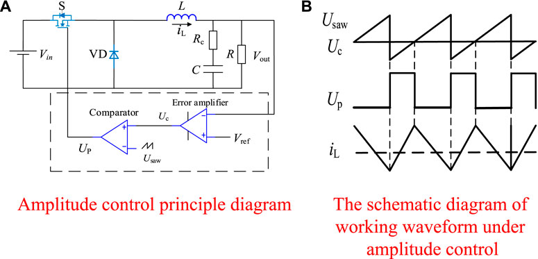
FIGURE 1. Buck converter variable amplitude control.
It can be seen from Figure 1A that the voltage-type control used the output voltage sampling as the input signal of the control loop. The direct proportional relationship between its input and output can be represented by (1):
where D is the duty cycle.
As shown in Figure 1B, the duty cycle of the switch tube drive signal Up was adjusted by changing the amplitude, and finally the purpose that the output follows the given was achieved.
The design and analysis of the traditional variable amplitude control is relatively simple. It can only be detected when the output voltage changes and feedback for correction, so the dynamic response speed is slow; due to the voltage amplitude control alone, only the voltage can be fed back. If there is a sudden current change in the circuit, the over-current situation has no protective effect; and it is impossible to set the working mode of the converter under the traditional control.
The single-voltage control is the most basic switch converter control method in the variable amplitude control, and it is also one of the most widely used control methods.
The variable frequency control principle of the Buck converter is shown in Figure 2. It was adjusted by changing the operating frequency of the switch tube. Its control principle can be represented by (2):
where ton is the on-time of the switch tube, and f is the operating frequency of the switch tube. ton remains unchanged.
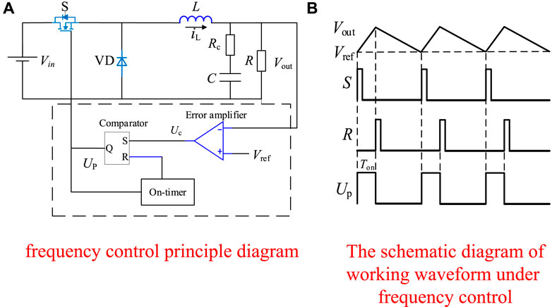
FIGURE 2. Buck converter variable frequency control.
Compared with the traditional variable amplitude control, the Buck variable frequency control has better dynamic performance; however, the control stability of this control method is not good, and it is affected by the equivalent series resistance of the output capacitor; at the same time, the control accuracy of the output voltage is poor, it is also impossible to accurately set the working mode of the converter.
In view of the shortcomings of the above methods, in order to further improve the system performance, this paper proposes a variable amplitude/frequency control method with the controllable mode, the control principle diagram is shown in Figure 3, and the control block diagram is shown in Figure 4.
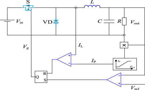
FIGURE 3. Schematic diagram of the variable amplitude/frequency control.
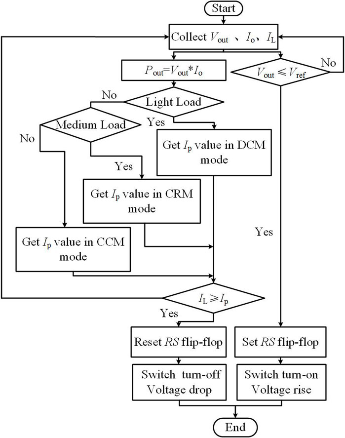
FIGURE 4. Block diagram of the variable amplitude/frequency control.
Under this control method, while realizing the fast dynamic response of the system, the operating mode of the converter could be precisely controlled according to the size of the load, and the current stress of the switch tube could be reduced.
In the schematic diagram shown in Figure 3, Vin and Vout are the input voltage and output voltage of the Buck converter respectively, IL is the inductor current, Io is the output current, Vg is the driving signal, S is the switch tube, VD is the diode, and L is the Inductor, C is the output capacitance, and R is the load resistance. In the outer loop control, the output voltage Vout and the reference voltage Vref passed through the voltage comparator to generate a driving signal to control the conduction of the switch tube; In the inner loop control, the output voltage Vout and the output current Io passed through the multiplier to obtain the output power Pout of the load, and Pout was converted by the function editor to obtain the corresponding inductor peak current Ip. Finally, the inductor peak current Ip and the inductor current IL passed through the current comparator to generate a driving signal to control the turn-off of the switch tube.
Based on the control strategy shown in Figure 4, the function of adjusting the system output could be achieved, and the system working mode could be precisely controlled. When the output voltage Vout dropped to the reference voltage Vref, the voltage comparator output a high level, the RS flip-flop was set, the Q terminal output a high level, a driving signal was generated, the switch S was controlled to turn on, and the output voltage Vout began to rise; At the same time, the output power Pout passed through the function editor, and the reference value Ip of the current comparator was generated according to the relationship between the output power and the peak current of the inductor. When the inductor current IL rose to the peak current Ip, the current comparator output a high level, the flip-flop was reset, the Q terminal output a low level, and the switch S was controlled to turn off.
Under the control method in this paper, when the inductor was determined, the circuit could work in the best operating mode under different loads, thereby reducing the current stress of the switch tube. Under a certain working condition, the on-off time of the switch tube was adjusted corresponding to different loads, and the frequency of the control signal was changed. At the same time, the peak reference value of the inductor current was also adjusted according to the load changes to ensure that the entire circuit worked under the set conditions.
The Buck converter with the variable amplitude and frequency control could realize the switching design of the circuit working mode and met the strict requirements of the system average efficiency and no-load standby. In this paper, according to the relationship between the peak inductor current Ip and the output power Pout, the function editor was used to design and change the parameters to adjust the operating frequency of the switch tube, and finally realize the selection and switching of the working mode of the Buck converter with the load change.
When the circuit inductor was fixed, if the circuit was to work in this mode, it needed to meet the conditions of (2):
where T represents the period of the switch tube, D is the duty cycle, L is the inductor, and R is the load.
The size of R indirectly reflected the size of the output power. When the output power satisfied Equation 2, the circuit would work in the CRM.
The output current can be expressed duty cycle D as (3):
toff is the turn-off time of the switch tube.
By combining the above equations, the relationship of the output power and the peak value of the inductor current can be derived as shown in (4):
From Equation 4, the relationship of the peak current Ip of the inductor current, the output power Pout, and the output voltage Vout could be obtained, thus, the curve of the relationship of Ip, Pout and Vout could be obtained, as shown in Figure 5. When the output voltage remained constant, the peak current Ip and the output power Pout had a linear relationship. Based on this, the design of the working conditions could be realized. When the relationship between the peak current Ip and the output power Pout satisfied Equation 4, the circuit worked in the critical mode; when the peak current Ip was constant, the output power Pout was lower than the corresponding peak current, the circuit would work in the discontinuous mode; when the peak current Ip was constant and the output power Pout was higher than the corresponding peak current Ip, the circuit would work in the continuous mode.
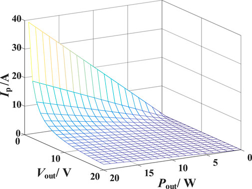
FIGURE 5. Relationship diagram of Ip, Pout, and Vout in the CRM.
The conditions for the circuit to operate in this mode are
When the output power satisfied the above, the circuit would work in the CCM. The control loop would adjust the inductor current peak value according to the load change to ensure that the circuit worked in the CCM.
The relationship between Ip and Pout in the CCM can be obtained as follows:
Figure 6 shows the relationship of Ip, Pout and Vin in the CCM. When the input voltage remained unchanged, when the output power increased, the peak value of the inductor current would increase accordingly. When the output power remained unchanged, the increase in the input voltage would cause the peak value of the inductor current to increase.
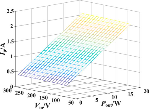
FIGURE 6. Relationship diagram of Ip, Pout, and Vout in the CCM.
The analysis showed that the conditions for the circuit to work in this mode are
In this mode, when the duty cycle D and the input voltage Vin met the constraints of the above, the circuit would work in the DCM.
When the circuit worked in the DCM, according to the Buck principle, the following can be obtained:
where δ is the duty cycle of the inductor current falling time, and δT is the continuation time for the switch tube to disconnect the inductor. Thus, the relationship between Ip and Pout in the DCM can be obtained as follows:
Figure 7 shows the relationship of Ip, Pout and Vin in the DCM. It can be seen from Figure 6 that when the input voltage remained unchanged, the peak value of the inductor current would make the same change with the output power; when the output power remained unchanged, the inductor current was inversely proportional to the input voltage.
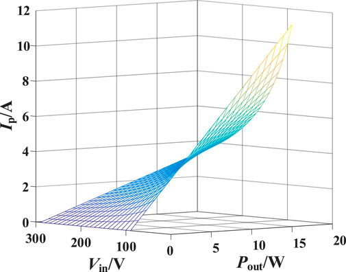
FIGURE 7. Relationship of Ip, Pout, and Vin in the DCM
When considering the influence of the parasitic parameters, the above control method is also applicable. The main circuit with the parasitic parameters is shown in Figure 8. Rs is the on-resistance of the switch tube, Rc is the equivalent resistance of the output capacitor, RL is the on-resistance of the inductor, and VD is the on-voltage drop of the diode.
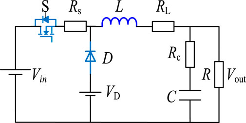
FIGURE 8. Buck converter topology of parasitic parameters.
Considering the parasitic parameters, the relationship between the inductor peak current and output power can be expressed by the following equation:
Where
Taking the CCM as an example, when the input voltage was constant, the relationship between the inductor current and the output power with the parasitic parameters is as follows:
Ip1 is the peak value of the inductor current with the parasitic parameters, and Ip2 is the peak value of the inductor current in the rational circuit.
It can be seen from Figure 9 that the influence of the circuit with the parasitic parameters on the relationship between the peak value of the inductor current and the output power could be approximately ignored.
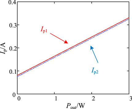
FIGURE 9. Relationship of Ip and Pout.
The control strategy proposed in this paper could change the peak value of the current and the working frequency by improving control degrees of freedom, which reduced the current stress of the switch tube controlled by the duty cycle alone.
Figure 9 shows that the optimal working mode under different conditions was selected to achieve the control effect of the lowest current stress of the switch tube.
In Figure 10A, with the output voltage being 12V, when the output power was less than 1.51W, the control circuit worked in the CRM; when the output power was greater than 1.51W, the control circuit worked in the CCM. In this control mode, the current stress of the switch tube could be reduced to the minimum, and its current stress could be expressed by the following:

FIGURE 10. Working condition diagram.
In Figure 10B, with the output voltage being 3V, when the output power is less than 0.21W, the control circuit worked in the DCM; when the output power was greater than 0.21W, the control circuit worked in the CCM. In this control mode, the current stress of the switch tube could be reduced to the minimum, and its current stress can be expressed by the following:
Through the variable amplitude and frequency control, the optimal working mode could be selected according to different circuit conditions, thereby reducing the current stress of the switch tube and accurately controlling the switching of circuit modes.
In this paper, the parameters of the Buck converter under the variable amplitude and frequency control were designed and verified by the simulation and experiments. Firstly, the circuit was designed to work in the single mode with the full load range, so that the feasibility of the control method in this paper could be verified. Secondly, the system was controlled to work in the optimal current stress mode in the full load range to improve the working performance of the converter. Finally, this paper conducted simulation through Matlab/Simulink, and built the experimental platform as shown in Figure 11 to verify the validity of this theory. The experimental parameters are shown in Table 1. The operating frequency of the traditional variable amplitude control circuit was set to 60kHz, and the period of the switch tube and the output voltage were stable and unchanged. The new control strategy improved the accuracy of the output voltage by changing the frequency and amplitude of the inductor current, while ensuring that the circuit could work in the set mode.
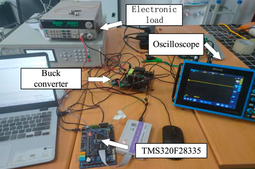
FIGURE 11. Photograph of experimental setup.
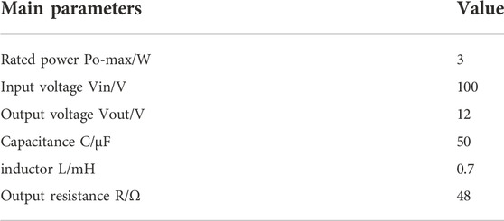
TABLE 1. Main parameters of the Buck converter with rated power of 3W
The simulation in Figure 12 verified that the circuit worked in the CCM, and the inductor current was in continuous mode under different loads. Under different loads, the circuit could work in the continuous mode under the full load and the heavy load, which showed the feasibility of the proposed control strategy. The peak value of the inductor current was adjusted for different loads. The simulation results were in line with the theoretical derivation. Different output powers generated the corresponding reference value of the peak current, and then control the peak value changes of the inner loop of the current.
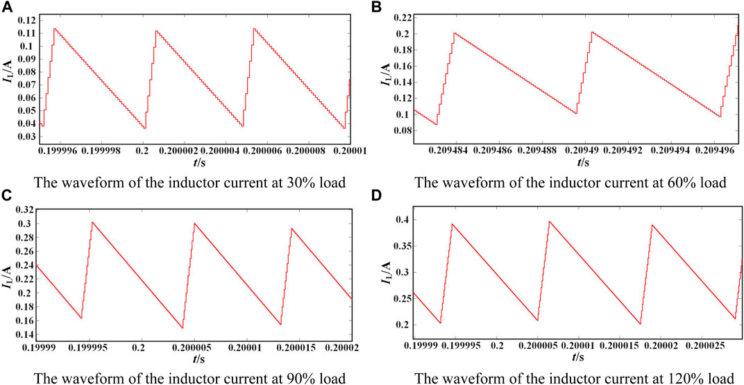
FIGURE 12. Inductor current waveforms with different loads in CCM at 3W rated power.
Figure 13 verified the precise switching control of the circuit operating modes. Figure 13A shows the circuit works in the DCM with 49% load. Figure 13 (b) shows that the circuit works in the CRM with 50% load. Figure 13 (c) shows that the circuit works in the CCM with 51% load. The working mode of the circuit could be accurately controlled by the variable frequency and the variable amplitude in this paper. The experimental results were in line with the theoretical derivation.
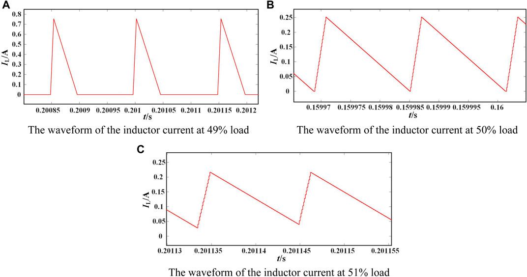
FIGURE 13. Inductor current waveforms with the mode switching at 3W rated power.
In order to verify the effectiveness of this method, the experimental verification with a power of 100W was added. The experimental parameters are shown in Table 2. In the case of the same hardware circuit, the current stress of the switch tube was compared with the traditional voltage single loop.
TABLE 2. Main parameters of the Buck converter with rated power of 100W
Figure 14 and Figure 15 are the waveforms diagram of the inductor current under the traditional control and the proposed control strategy of this paper with different loads, 3W and 100W respectively. Using the control strategy in this paper, it could be found that with 20% and 40% load, the circuit worked in the CRM, and with 60% and 80% load, the circuit worked in the CCM. The control circuit of the new method worked in the optimal working mode of the current stress, and the current stress was obviously optimized compared with the results under the traditional voltage loop. The current stress comparison results of the control strategy in this paper and the traditional control strategy under the rated power of 3W and 100W are shown in Table 3 and Table 4, respectively.
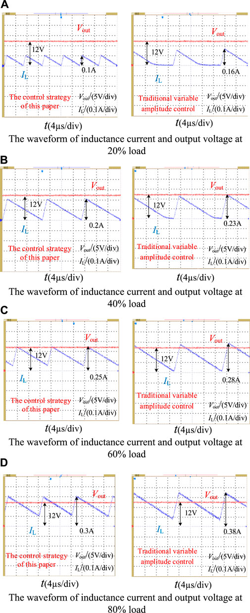
FIGURE 14. Waveforms under different loads at 3W rated power.
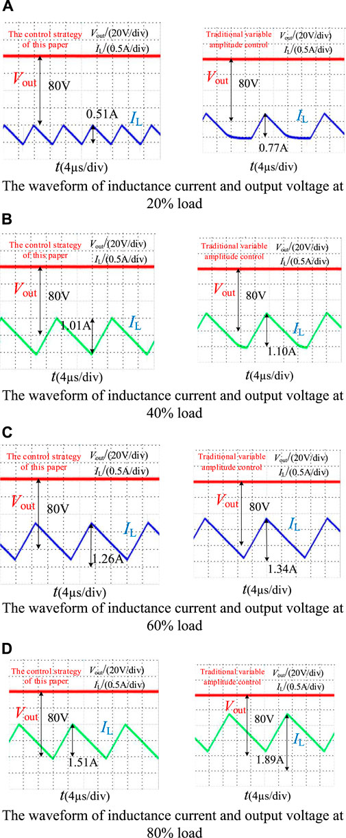
FIGURE 15. Waveforms under different loads at 100W rated power.
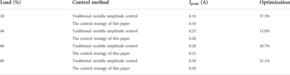
TABLE 3. Comparative analysis of current stress with rated power of 3W
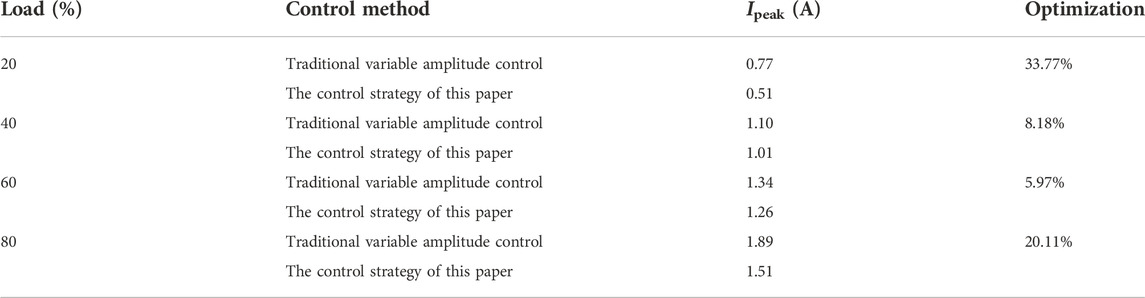
TABLE 4. Comparative analysis of current stress with rated power of 100W
Table 5 shows a comparison of experimental data and theoretical values to demonstrate the effectiveness of the new method. No matter the output power is 3W or 100W, the peak current of the inductor current can match the theoretical value, which can optimize the stress of the device and improve the efficiency of the system.

TABLE 5. Comparative between the theoretical value and the actual Value``
The control circuit of the new method worked in the optimal working mode of the current stress, and the current stress was obviously optimized compared with the results under the traditional voltage loop. The current stress transformation trend under the full load range is shown in Figure 16, from which it can be seen that under the control strategy of this paper, the current stress can be significantly optimized.
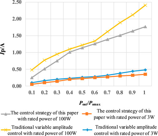
FIGURE 16. Comparative analysis of current stress.
Figure 17 is a comparison diagram of the efficiency under the traditional control and the control strategy of this paper with different loads. The analysis showed that since the circuit worked in the mode with the smallest current stress, the conduction loss was effectively reduced, the average efficiency of the converter was higher than that of the traditional control strategy, and the efficiency could be increased by 0.5% with the full load. Under light load conditions, the efficiency would decrease due to the increased proportion of the system stray losses. Under the control strategy in this paper, the light-load efficiency was significantly improved compared with the light-load efficiency under the traditional control strategy, and the average efficiency of the converter in the full load range was also optimized, and the average efficiency was improved by 2.21%.
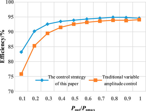
FIGURE 17. Efficiency comparisons under different loads.
In this paper, the variable amplitude and frequency control strategy is proposed to precisely control the working mode of the converter, and the control accuracy of the converter could be improved by adding control degrees of freedom. It solved the problem of large current stress in the traditional variable amplitude control strategy, and meanwhile improved the average efficiency of the system. In this paper, this control strategy was applied to the Buck converter. When the load changes in the full range, when the input power also changes at the same time, how to further ensure that the circuit works in the optimal mode, this can be in the follow-up study in-depth analysis. Through the theoretical analysis and experimental verification, the conclusion is as follows:
1) The established control model of the inductor current peak value and output power could control the working mode of the converter and improved the accuracy of the converter control.
2) The mode with the optimal current stress was selected according to the load changes to ensure the minimum current stress of the switch tube, and the current stress in the full load range was increased up to 37.5%.
3) The light-load efficiency of the converter was significantly improved, and the average efficiency in the full-load range was also optimized, increasing by 2.21%.
The original contributions presented in the study are included in the article/Supplementary material, further inquiries can be directed to the corresponding author.
Conceptualization, NL; methodology, NL, ZL, and YC; software, ZL; validation, ZL; resources, NL; data curation, NL, DW, ZX, and YZ; writing—original draft preparation, ZL; writing—review and editing, NL, ZL, and YC; supervision, DW, ZX, and YZ; funding acquisition, NL. All authors have read and agreed to the published version of the manuscript.
National Natural Science Foundation of China (52177193); Key Research and Development Program of Shaanxi Province(2022GY-182); China Scholarship Council (CSC) State Scholarship Fund International Clean Energy Talent Project (Grant No. [2018]5046,[2019]157). Xi 'an Science and Technology Plan Project (22GXFW0078).
The authors declare that the research was conducted in the absence of any commercial or financial relationships that could be construed as a potential conflict of interest.
All claims expressed in this article are solely those of the authors and do not necessarily represent those of their affiliated organizations, or those of the publisher, the editors and the reviewers. Any product that may be evaluated in this article, or claim that may be made by its manufacturer, is not guaranteed or endorsed by the publisher.
Abdelhamid, E., Bonanno, G., Corradini, L., Mattavelli, P., and Agostinelli, M. (2019). Stability properties of the 3-level flying capacitor buck converter under peak or valley current programmed control. IEEE Trans. Power Electron. 34 (8), 8031–8044. Aug. doi:10.1109/tpel.2018.2877943
Al-Baidhani, H., Salvatierra, T., Ordóñez, R., and Kazimierczuk, M. K. (2021). Simplified nonlinear voltage-mode control of PWM DC-DC buck converter. IEEE Trans. Energy Convers. 36 (1), 431–440. doi:10.1109/tec.2020.3007739
Alexandru, I. C., and Mircea, B. (2019). “Analysis and design of a current mode buck converter with digitally controlled output voltage,” in 2019 International Semiconductor Conference. Sinaia, Romania: CAS, 309–312. doi:10.1109/SMICND.2019.8923781
Asad, M., Singha, A. K., and Rao, R. M. S. (2022). Dead time optimization in a GaN-based buck converter. IEEE Trans. Power Electron. 37 (3), 2830–2844. doi:10.1109/tpel.2021.3116126
Calam, R. C. M., Hora, J. A., Gerasta, O. J. L., Zhu, X., and Dutkiewicz, E. (2019). “A self-calibrating off-time controller for WSN/IoT synchronous non-inverting buck-boost DC-to-DC converter application,” in 2019 IEEE International Circuits and Systems Symposium (ICSyS), 1–4.
Chen, J. -J., Hwang, Y. -S., Ku, Y., Li, Y. -H., and Chen, J. -A. (2021). A current-mode-hysteretic buck converter with constant-frequency-controlled and new active-current-sensing techniques. IEEE Trans. Power Electron. 36 (3), 3126–3134. doi:10.1109/tpel.2020.3017809
Chen, W., and Lai, J. (2019). A novel dynamic ramp valley control in a current-mode adaptive on-time controller for the on-chip buck converter. IEEE Trans. Power Electron. 34 (6), 5830–5841. doi:10.1109/tpel.2018.2866737
Fang, C., and Redl, R. (2015). Subharmonic instability limits for the peak-current-controlled buck converter with closed voltage feedback loop. IEEE Trans. Power Electron. 30 (2), 1085–1092. Feb. doi:10.1109/tpel.2014.2312354
Hwang, Y. -S., Chen, J. -J., Ku, Y. -T., and Yang, J. -Y. (2021). An improved optimum-damping current-mode buck converter with fast-transient response and small-transient voltage using new current sensing circuits. IEEE Trans. Ind. Electron. 68 (10), 9505–9514. Oct. doi:10.1109/tie.2020.3020030
Kim, D., and Shin, J. -W. (2021). Dynamic response of buck converter with auxiliary current control: Analysis and design of practical implementation. IEEE Trans. Power Electron. 36 (12), 13917–13929. Dec. doi:10.1109/tpel.2021.3087607
Kim, J. -S., Yoon, J. -O., and Choi, B. -D. (2022). A high-light-load-efficiency low-ripple-voltage PFM buck converter for IoT applications. IEEE Trans. Power Electron. 37 (5), 5763–5772. doi:10.1109/tpel.2021.3131594
Kim, S. -K., Kim, K. -C., and Ahn, C. K. (2022). Output-voltage-tracking control for buck converters using variable convergence rate mechanism without current feedback. IEEE Trans. Ind. Electron. 69 (3), 2938–2946. doi:10.1109/tie.2021.3065610
Lin, J., Su, M., Sun, Y., Li, X., Xie, S., Zhang, G., et al. (2022). Accurate loop gain modeling of digitally controlled buck converters. IEEE Trans. Ind. Electron. 69 (1), 725–739. doi:10.1109/tie.2021.3050389
Liu, X., Wu, B., and Xiu, L. (2022). A fast positive-sequence component extraction method with multiple disturbances in unbalanced conditions. IEEE Trans. Power Electron. 37 (8), 8820–8824. doi:10.1109/tpel.2022.3161734
Liu, X., Xiong, L., Wu, B., Qian, Y., and Liu, Y. (2022). Phase locked-loop with decaying DC transient removal for three-phase grids. Int. J. Electr. Power & Energy Syst. 143, 108508. doi:10.1016/j.ijepes.2022.108508
Nan, C., Ayyanar, R., and Xi, Y. (2018). A 2.2-MHz active-clamp buck converter for automotive applications. IEEE Trans. Power Electron. 33 (1), 460–472. doi:10.1109/tpel.2017.2672522
Nguyen, M., Tran, T., and Lim, Y. (2019). A family of PWM control strategies for single-phase quasi-switched-boost inverter. IEEE Trans. Power Electron. 34 (2), 1458–1469. Feb. doi:10.1109/tpel.2018.2831674
Redl, R., and Sun, J. (2009). Ripple-based control of switching regulators—an overview. IEEE Trans. Power Electron. 24 (12), 2669–2680. Dec. doi:10.1109/tpel.2009.2032657
Ripamonti, G., Saggini, S., Corradini, L., Rizzolatti, R., Faccio, F., Michelis, S., et al. (2019). A dual-edge pulsewidth modulator for fast dynamic response DC–DC converters. IEEE Trans. Power Electron. 34 (1), 28–32. doi:10.1109/tpel.2018.2836385
Sun, Q., Ma, Y., Ye, Z., Wang, X., and Zhang, H. (2019). A pseudo-constant frequency constant on-time buck converter with internal current ripple injection and output DC offset cancellation. IEEE Access 7, 175443–175453. doi:10.1109/ACCESS.2019.2957784
Talebian, I., Alavi, P., Marzang, V., Babaei, E., and Khoshkbar-Sadigh, A. (2022). Analysis, design, and investigation of a soft-switched buck converter with high efficiency. IEEE Trans. Power Electron. 37 (6), 6899–6912. doi:10.1109/tpel.2021.3132463
ul Ain, Q., Khan, D., Jang, B. G., Basim, M., Shehzad, K., Asif, M., et al. (2021). A high-efficiency fast transient COT control DC–DC buck converter with current reused current sensor. IEEE Trans. Power Electron. 36 (8), 9521–9535. Aug. doi:10.1109/tpel.2021.3052198
Wang, Y., Ruan, X., Leng, Y., and Li, Y. (2019). Hysteresis current control for multilevel converter in parallel-form switch-linear hybrid envelope tracking power supply. IEEE Trans. Power Electron. 34 (2), 1950–1959. doi:10.1109/tpel.2018.2835640
Wang, Y., Xu, J., and Yin, G. (2019). Cross-regulation suppression and stability analysis of capacitor current ripple controlled SIDO CCM buck converter. IEEE Trans. Ind. Electron. 66 (3), 1770–1780. doi:10.1109/tie.2018.2838103
Yang, W. -H., Yang, H. -A., Huang, C. -J., Chen, K. -H., and Lin, Y. -H. (2018). A high-efficiency single-inductor multiple-output buck-type LED driver with average current correction technique. IEEE Trans. Power Electron. 33 (4), 3375–3385. doi:10.1109/tpel.2017.2709039
Keywords: variable frequency control, variable amplitude control, current stress, Buck converter, efficiency
Citation: Li N, Li Z, Cao Y, Wei D, Xiao Z and Zhang Y (2023) Current stress optimization control strategy of the buck topology with the variable frequency/amplitude mode. Front. Energy Res. 10:1087775. doi: 10.3389/fenrg.2022.1087775
Received: 02 November 2022; Accepted: 18 November 2022;
Published: 10 January 2023.
Edited by:
Weihao Hu, University of Electronic Science and Technology of China, ChinaReviewed by:
Zhao Zhihong, Nanjing University of Science and Technology, ChinaCopyright © 2023 Li, Li, Cao, Wei, Xiao and Zhang. This is an open-access article distributed under the terms of the Creative Commons Attribution License (CC BY). The use, distribution or reproduction in other forums is permitted, provided the original author(s) and the copyright owner(s) are credited and that the original publication in this journal is cited, in accordance with accepted academic practice. No use, distribution or reproduction is permitted which does not comply with these terms.
*Correspondence: Ning Li, bGluaW5nODNAeGF1dC5lZHUuY24=
Disclaimer: All claims expressed in this article are solely those of the authors and do not necessarily represent those of their affiliated organizations, or those of the publisher, the editors and the reviewers. Any product that may be evaluated in this article or claim that may be made by its manufacturer is not guaranteed or endorsed by the publisher.
Research integrity at Frontiers
Learn more about the work of our research integrity team to safeguard the quality of each article we publish.