 Shangzhou Zhang1,2*
- 1College of Electronic Information and Electrical Engineering, Shangluo University, Shangluo, China
- 2Research Center of Shangluo Distributed New Energy Application Technology, Shangluo, China
The SiC MOSFET has lower conduction loss and switching loss than the Si IGBT, which helps to improve the efficiency and power density of the converter, especially for those having strict requirements for volume and weight, for example, electrical vehicles (EVs), on-board chargers (OBCs), and traction drive systems (TDS). However, the faster switching speed will cause overshoot and oscillation problems, which will affect the efficiency and security of the SiC devices and power electronic systems. For the SiC MOSFET to be better used, combining a theoretical analysis, the double-pulse test platform is built. The controllable principles of SiC MOSFETs are validated. The turn-on and turn-off delay, switching delay, switching di/dt, switching du/dt, switching overshoot, and switching loss of SiC MOSFETs under different driving and parasitic parameters are explored. Finally, some valuable suggestions for designing are proposed for a better application of the SiC MOSFET.
1 Introduction
The SiC MOSFET is a typical wide-bandgap power semiconductor device (Zeng and Li, 2018). Compared with the Si IGBT, the SiC MOSFET has lower conduction loss and switching loss, which means the efficiency of the converter can be improved, especially in high-frequency applications. At the same time, the operation temperature of the SiC MOSFET is higher than that of the Si IGBT, which reduces the size of the heat sink, so the power density of the converter can be improved too. Therefore, the SiC MOSFET is considered to have potential in electric vehicles, photovoltaic power generation, and high-frequency power supplies (Camacho et al., 2017; Xie et al., 2021). However, due to the high switching speed of the SiC MOSFET, the current and voltage overshoot would reduce the electromagnetic compatibility of the converter. In addition, the overshoots and oscillations will accelerate the aging of the device and eventually cause its failure (Sun et al., 2021).
Various literature works studied the overshoots and oscillations of the SiC MOSFET during the switching transients. The influence of the source inductance and drain inductance on the overshoots is reported in Li et al. (2016) and Yang et al. (2022). Considering different parasitic parameters, Bonyadi et al. (2015), Wang et al. (2019), and Talesara et al. (2020) provided the behavior model of the half bridge applying SiC MOSFETs, and the simulation and experiment results show that the overshoots and oscillations are mainly caused by the parasitic inductance in the loop, which should be reduced as much as possible. The analytical model is proposed in Stark et al. (2021) to characterize the switching behaviors of the SiC MOSFET. Riccio et al. (2018) confirmed that the gate driving resistor can damp the oscillation of the SiC MOSFET. However, comprehensive research about the influence of driving parameters and parasitic parameters on the switching behaviors of the SiC MOSFET is lacking among the existing studies, and there is no conductive guidance about designing the gate driver.
In this study, comprehensive research about the influence of driving parameters and parasitic parameters on the switching behaviors of the SiC MOSFET is carried out, which includes the gate resistance Rg, the gate–source capacitance Cgs, the gate–drain capacitance Cgd, the drain–source Cds, the gate inductance Lg, the source inductance Ls, and the loop inductance Lloop. The measured results show that the switching behavior of the SiC MOSFET is controlled by these parameters from different aspects and should be given special attention during the designing period.
This paper is organized as follows. In Section 2, the switching behavior of the SiC MOSFET is studied. The dynamic characteristics of the SiC MOSFET with different driving and parasitic parameters are explained in Section 3. Finally, the conclusion is drawn in Section 4.
2 Switching behavior
2.1 Comparison between SiC and Si devices
The SiC MOSFET is considered a good substitute for the Si IGBT because better static and dynamic characteristics can be achieved in the SiC MOSFET. Table 1 shows the comparison of the key parameters between the SiC MOSFET and the Si IGBT. The Si IGBT (IXGH20N120B) and SiC MOSFET (C2M0080120D) are selected in the comparison because the power levels of the two devices are similar. In terms of the static characteristic, the on-state resistance of the SiC MOSFET is 80 mΩ, while the on-state voltage drop of the Si IGBT is 2.9 V, so the conduction loss of the SiC MOSFET is lower than that of the Si IGBT when the continuous conducting current is lower than 36.25 A. In terms of the dynamic characteristic, the gate charge and input capacitance of the SiC MOSFET are 62 nC and 950 pF, respectively, while those parameters of the Si IGBT are 72 nC and 1,700 pF, respectively. The lower gate charge and input capacitance of the SiC MOSFET mean that the SiC MOSFET can switch at a higher speed and frequency than those of the Si IGBT. It can be seen in Table 1 that the turn-on and turn-off switching losses of the SiC MOSFET are lower than those of the Si IGBT due to the high switching speed of the SiC MOSFET.
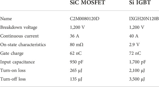
TABLE 1. Comparison of key parameters between the SiC MOSFET and Si IGBT.
The high switching speed of the SiC MOSFET will cause overshoots, oscillations, and EMI during the ns-level switching transient. The driving parameters will influence the charging speed of the input capacitance, and the parasitic parameters will form resonant networks. In order to investigate the dynamic characteristics of the SiC MOSFET in detail, the double pulse test is carried out as follows.
2.2 Double pulse test
The dynamic characteristics of the power device are usually tested on the double pulse test (DPT) platform, which is built into PSpice software. The DPT setting is shown in Figure 1, where VBUS is the bus voltage, CBUS is the bus capacitor, Lload is the load inductor, Df is the body diode of the SiC MOSFET, Lloop is the parasitic inductance in the loop, Lg is the inductance in the gate loop, Ls is the source inductance of the device, Cgs is the gate–source capacitance, Cgd is the gate–drain capacitance, Cds is the drain–source capacitance, Rg is the driving resistance, Vg is the positive driving voltage, and Ve is the negative driving voltage (Duan et al., 2018; Qin et al., 2018). The first driving pulse is used to establish the load current by turning on the SiC MOSFET, and the second pulse is used to observe the dynamic characteristics of the SiC MOSFET. It should be noted that Rg, Cgs, Cgd, and Cds are changeable, and the parasitic inductances Lloop, Lg, and Ls are controllable during the design period.
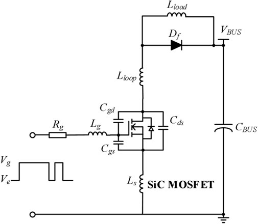
FIGURE 1. Double pulse test setting.
2.3 Switching behaviors
The switching behavior of the SiC MOSFET can be represented by the waveforms of the gate–source voltage ugs, the drain–source voltage uds, and the drain current id (Li et al., 2017; Huang et al., 2021; Xiong et al., 2022a). The key waveforms of the SiC MOSFET are shown in Figure 2.

FIGURE 2. Switching behavior of the SiC MOSFET.
It can be seen from Figure 2 that the turn-on behavior and turn-off behavior of the SiC MOSFET have the similar and symmetrical relationship. Both the turn-on and turn-off periods have five typical transients, namely, the delay period, the di/dt period, the du/dt period, the overshoot and oscillation period, and the state period (As detailed in Appendix A). The slew rate of the drain current is the cause of the overshoot for id and uds. In the turn-on transient, the reverse recovery of the body diode will cause the current overshoot, and it has
where Ipeak is the peak value of id, Qrr is the reverse recovery charge of the body diode, and S is the snappiness factor of the body diode. In the turn-off transient, the parasitic inductance in the loop will cause an obvious overshoot in uds (Wu et al., 2020; Zhao et al., 2020a; Qi et al., 2021), and it has
The slew rate of the drain–source voltage uds is the cause for the crosstalk phenomena. When the SiC MOSFET switches at high switch, the displacement current through Cgd will cause the false turn-on of the synchronization device (Roy and Basu, 2021), and the displacement current igd can be expressed as follows:
The switching behavior of the SiC MOSFET is directly related to the reliability of the device (Chen et al., 2021; Rashid et al., 2021). Therefore, it is important to carry out the comprehensive research about the influence of driving parameters and parasitic parameters on the switching behaviors of the SiC MOSFET.
3 Experiment results
The DPT prototype is applied to investigate the dynamic characteristics of the SiC MOSFET, as shown in Figure 3. The load inductance Lload is equal to 200 μH, the tested device is C2M0080120D of CREE, the bus voltage is equal to 400 V, and the load current is 20 A. The oscilloscope is DPO3054 (500 MHz), the current probe is TCP305 A (30 MHz), and the voltage probe is P6139 A (500 MHz). The bandwidth of the probe is enough for measuring the transients of uds and id.
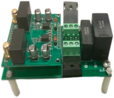
FIGURE 3. DPT prototype.
3.1 Influence of Rg
The gate driving Rg can be selected during the designing period. Figure 4 shows the waveforms of id and uds with different Rg, and Figure 5 presents the dynamic characteristics of the SiC MOSFET with different Rg. It is obvious that with the increase in Rg, the turn-on and turn-off delay of the device will increase because the charging time of the input capacitance increases. The slew rate of id and uds decreases with the increase of Rg, so the overshoot decreases and the device can operate at a slower speed. It is evident that both turn-on and turn-off losses increase with a larger Rg. Therefore, the worst efficiency of the converter occurs when a relatively large Rg is selected.
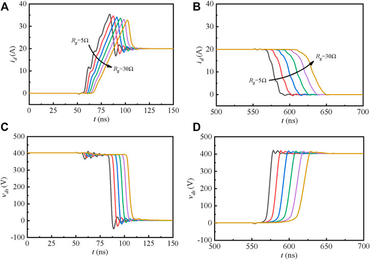
FIGURE 4. Influence of Rg on the switching behavior of the SiC MOSFET. (A) Turn-on id. (B) Turn-off id. (C) Turn-on uds. (D) Turn-off uds.
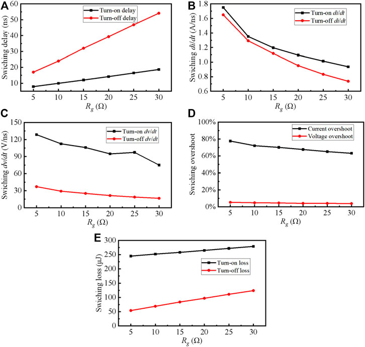
FIGURE 5. Dynamic characteristics of the SiC MOSFET with different Rg. (A) Switching delay. (B) Switching di/dt. (C) Switching du/dt. (D) Switching overshoot. (E) Switching loss.
3.2 Influence of Cgs
The gate–source capacitance Cgs determines the delay time and the value of di/dt. As shown in Figure 6 and Figure 7, the influence of Cgs on the dynamic characteristics of the SiC MOSFET is similar to that of Rg. The switching speed will decrease if a larger Cgs is selected. It should be noted that the value of Cgs has no significant influence on the slew rate of uds.
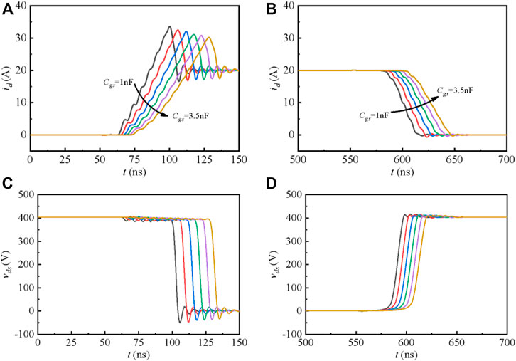
FIGURE 6. Influence of Cgs on the switching behavior of the SiC MOSFET. (A) Turn-on id. (B) Turn-off id. (C) Turn-on uds. (D) Turn-off uds.
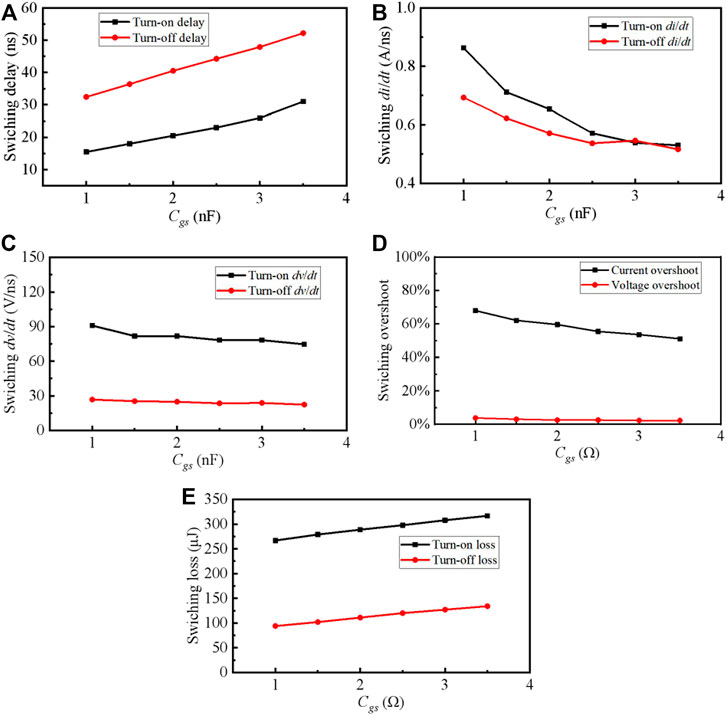
FIGURE 7. Dynamic characteristics of the SiC MOSFET with different Cgs. (A) Switching delay. (B) Switching di/dt. (C) Switching du/dt. (D) Switching overshoot. (E) Switching loss.
3.3 Influence of Cgd
The gate–drain capacitance Cgd determines the value of du/dt, which is also called the “Miller capacitance.” The value of Cgd is far lower than the value of Cgs and Cds, and a little change in Cgd will cause a significant change in the value of du/dt. Figure 8 shows the waveforms of id and uds with different Cgd, and Figure 9 presents the dynamic characteristics of the SiC MOSFET with different Cgd. It can be seen that delay and di/dt have no obvious relationship with the value of Cgd. However, du/dt will decrease with the increase of Cgd, which will cause an increase in switching losses in turn. It should be noted that though the value of du/dt decreases with a larger Cgd, no significant optimization of overshoot occurs, and the risk of false turn-on will increase.
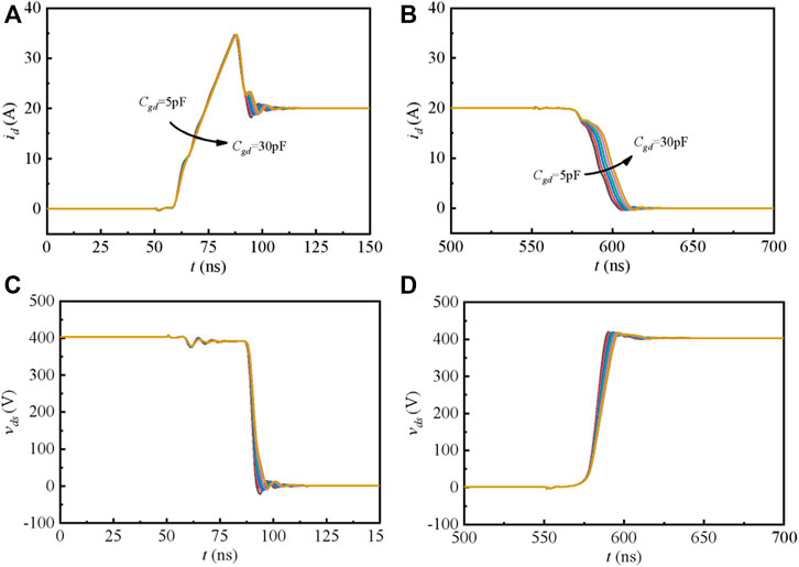
FIGURE 8. Influence of Cgd on the switching behavior of the SiC MOSFET. (A) Turn-on id. (B) Turn-off id. (C) Turn-on uds. (D) Turn-off uds.
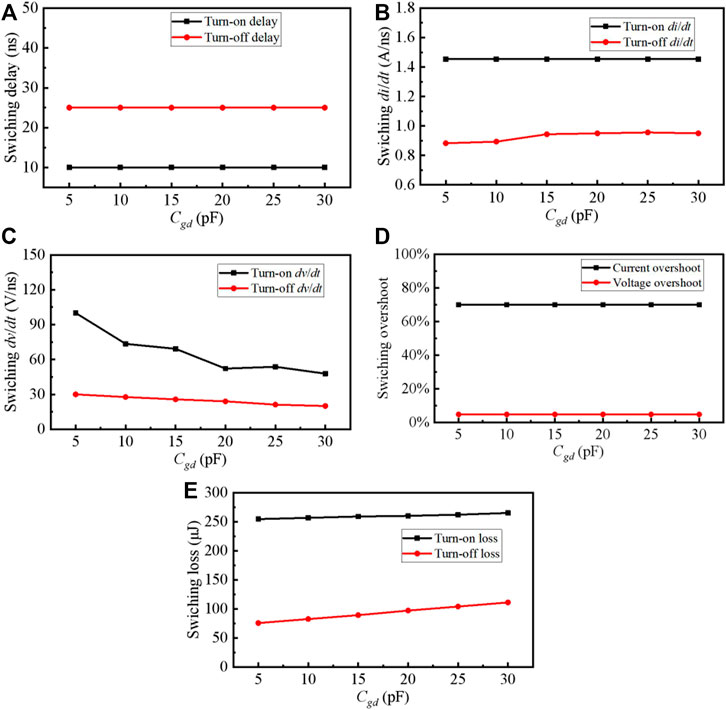
FIGURE 9. Dynamic characteristics of the SiC MOSFET with different Cgd. (A) Switching delay. (B) Switching di/dt. (C) Switching du/dt. (D) Switching overshoot. (E) Switching loss.
3.4 Influence of Cds
The drain–source capacitance Cds can influence the value of du/dt, and there is no necessary relationship between Cds, delay, and di/dt. The additional Cds is applied to achieve the soft turn-off by increasing Cds. As shown in Figure 10 and Figure 11, both turn-on and turn-off du/dt will decrease with the increase of Cds, and the turn-off loss and turn-off voltage overshoot will decrease as a result. However, the energy stored in Cds during the turn-off period will cause a significant current overshoot during the turn-on period, which means an obvious increase in the turn-on loss.
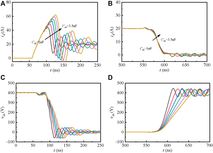
FIGURE 10. Influence of Cds on the switching behavior of the SiC MOSFET. (A) Turn-on id. (B) Turn-off id. (C) Turn-on uds. (D) Turn-off uds.
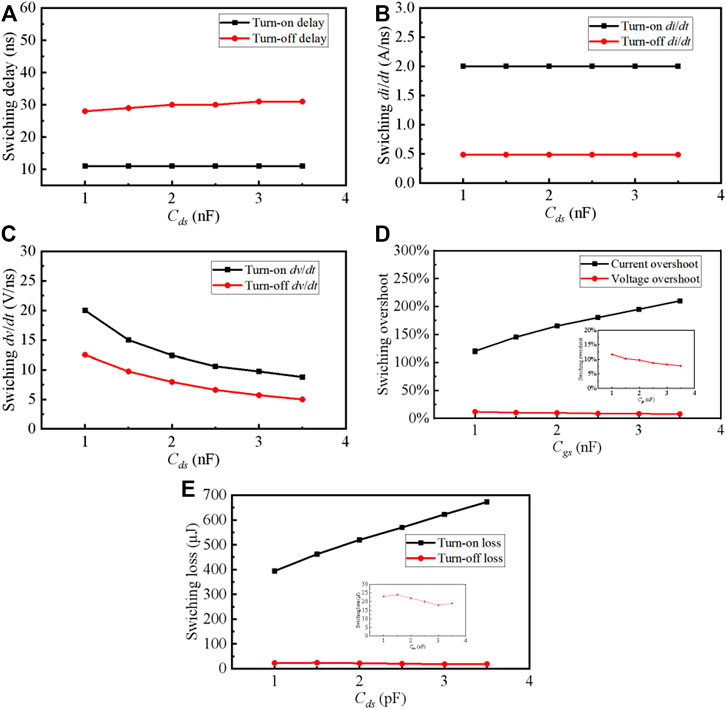
FIGURE 11. Dynamic characteristics of the SiC MOSFET with different Cds. (A) Switching delay. (B) Switching di/dt. (C) Switching du/dt. (D) Switching overshoot. (E) Switching loss.
3.5 Influence of Lg
The gate inductance Lg is caused by the PCB trace of the gate loop. As shown in Figure 12, the value of Lg has a minor influence on the dynamic characteristics of the SiC MOSFET. However, Lg should be reduced as much as possible because Lg will result in the overshoot of ugs, which risks the reliability of the gate.
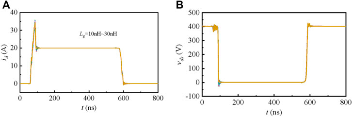
FIGURE 12. Influence of Lg on the switching behavior of the SiC MOSFET. (A) Turn-on and Turn-off of id. (B) Turn-off uds.
3.6 Influence of Lloop
The gate inductance Lloop is caused by the PCB trace of the power loop. It is different to cancel the Lloop, even though the relatively short PCB trace is designed. The most significant drawback brought by Lloop is the larger voltage overshoot, which will cause the device to breakdown. As shown in Figure 13 and Figure 14, the value of Lloop only influences the oscillation frequency and the voltage overshoot. In order to enhance the reliability of the SiC MOSFET, Lloop should be reduced as much as possible. It should be noted that a larger Lloop will result in lower turn-on loss because the drain–source voltage will drop during the di/dt period. At the same time, the turn-off loss will increase with the larger Lloop due to the additional loss from the voltage overshoot.
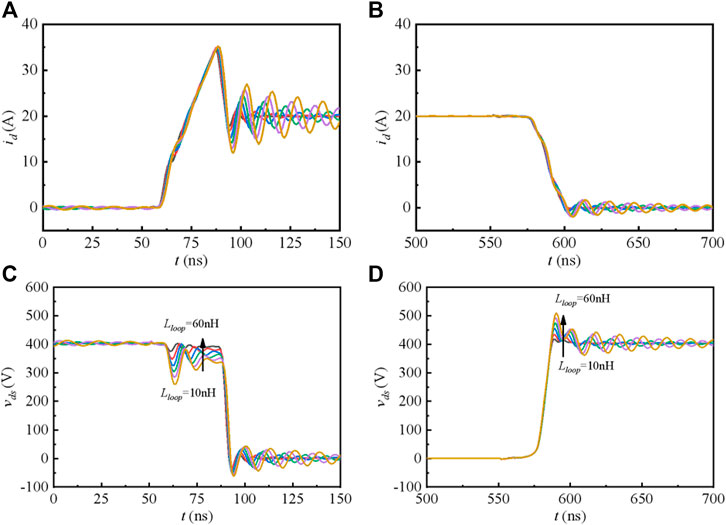
FIGURE 13. Influence of Lloop on the switching behavior of the SiC MOSFET. (A) Turn-on id. (B) Turn-off id. (C) Turn-on uds. (D) Turn-off uds.
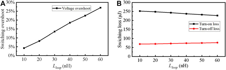
FIGURE 14. Dynamic characteristics of the SiC MOSFET with different Lloop. (A) Switching overshoot. (B) Switching loss.
3.7 Influence of Ls
The source inductance Ls exists in the gate loop and the power loop. As shown in Figure 15 and Figure 16, when the drain current id changes sharply, the induced voltage on Ls will slow down the switching speed as a negative feedback effect. Therefore, the larger Ls will cause lower di/dt during the switching transients. In order to reduce the switching losses, new type packages are provided by manufacturers, such as TO-247-4 and TO-263-7.
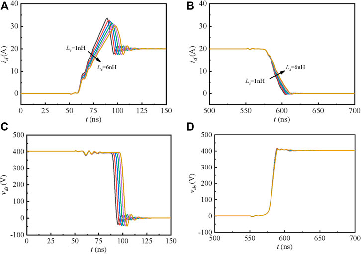
FIGURE 15. Influence of Ls on the switching behavior of the SiC MOSFET. (A) Turn-on id. (B) Turn-off id. (C) Turn-on uds. (D) Turn-off uds.
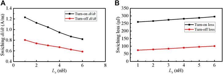
FIGURE 16. Dynamic characteristics of the SiC MOSFET with different Ls. (A) Switching di/dt. (B) Switching loss.
4 Conclusion
The SiC MOSFET is widely used in high-frequency and high-temperature applications, which helps to improve the efficiency and power density of the converter. However, the parasitic parameters will inevitably cause overshoot and oscillation of id and uds, which reduce the reliability of the SiC MOSFET. In this study, comprehensive research about the influence of driving parameters and parasitic parameters on the switching behaviors of the SiC MOSFET is carried out, and some valuable conclusions drawn are as follows:
1) The parasitic inductance should be reduced as much as possible by optimizing PCB traces and applying advanced packages
2) Different driving parameters will cause different dynamic responses of the SiC MOSFET, which should be considered according to special applications, respectively
3) The increase in Cgd is not recommended due to the higher risk of crosstalk
The influences of circuit parameters on the switching behaviors of the SiC MOSFET are listed as shown in Table 2.
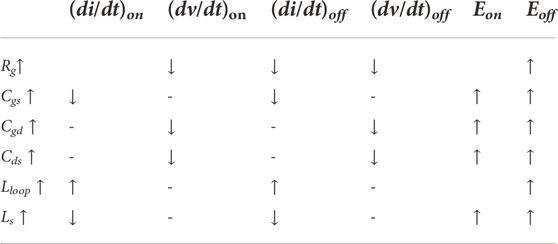
TABLE 2. Influences of circuit parameters on the switching behaviors.
Data availability statement
The original contributions presented in the study are included in the article/Supplementary Material; further inquiries can be directed to the corresponding author.
Author contributions
SZ: conceptualization, formal analysis, data curation, writing—original draft, visualization, and funding acquisition.
Funding
This work was supported by the Education Department Project of Shaanxi Province, China (20JK0614), and the Science and Technology Bureau Project of Shangluo City, China (2021-Z-0016).
Conflict of interest
The author declares that the research was conducted in the absence of any commercial or financial relationships that could be construed as a potential conflict of interest.
Publisher’s note
All claims expressed in this article are solely those of the authors and do not necessarily represent those of their affiliated organizations, or those of the publisher, the editors, and the reviewers. Any product that may be evaluated in this article, or claim that may be made by its manufacturer, is not guaranteed or endorsed by the publisher.
Appendix A:
The turn-on current oscillation and the turn-off voltage oscillation are two critical phenomena when describing the switching behaviors of the SiC MOSFET (Li et al., 2020). The turn-on current resonance angle frequency and the resonance damping of the SiC MOSFET can be expressed as follows:
The turn-off voltage resonance angle frequency and the resonance damping of the SiC MOSFET can be expressed as follows (Liu et al., 2016; Mukunoki et al., 2018):
where CL is the output capacitance of the freewheeling diode and RL is the equivalent on-state resistance of the freewheeling diode.
References
Bonyadi, R., Alatise, O., Jahdi, S., Hu, J., Ortiz Gonzalez, J. A., Ran, L., et al. (2015). Compact electrothermal reliability modeling and experimental characte- rization of bipolar latchup in SiC and CoolMOS power MOSFETs. IEEE Trans. Power Electron. 30 (12), 6978–6992. doi:10.1109/tpel.2015.2388512
Camacho, A. P., Sala, V., Ghorbani, H., and Romeral, L. (2017). A novel active gate driver for improving SiC MOSFET switching trajectory. IEEE Trans. Ind. Electron. 11, 9032–9042. doi:10.1109/TIE.2017.2719603
Chen, X., Chen, W., Yang, X., Ren, Y., and Qiao, L. (2021). Common-mode EMI mathematical modeling based on inductive coupling theory in a power module with parallel-connected SiC MOSFETs. IEEE Trans. Power Electron. 36 (6), 6644–6661. doi:10.1109/TPEL.2020.3046658
Duan, Z., Fan, T., Wen, X., and Zhang, D. (2018). Improved SiC power MOSFET model considering nonlinear junction capacitances. IEEE Trans. Power Electron. 33 (3), 2509–2517. doi:10.1109/tpel.2017.2692274
Huang, H., Wang, N., Wu, J., and Lu, T. (2021). Radiated disturbance characteristics of SiC MOSFET module. J. Power Electron. 21 (2), 494–504. doi:10.1007/s43236.020-00187-4
Li, H., Munk-Nielsen, S., Beczkowski, S., and Wang, X. (2016). A novel DBC layout for current imbalance mitigation in SiC MOSFET multichip power modules. IEEE Trans. Power Electron. 31 (12), 8042–8045. doi:10.1109/tpel.2016.2562030
Li, X., Jiang, J., Huang, A. Q., Guo, S., Deng, X., Zhang, B., et al. (2017). A SiC power MOSFET loss model suitable for high-frequency applications. IEEE Trans. Ind. Electron. 64 (10), 8268–8276. doi:10.1109/tie.2017.2703910
Li, X., Lu, Y., Ni, X., Wang, S., Zhang, Y., and Tang, X. (2020). Novel driver circuit for switching performance improvements in SiC MOSFETs. J. Power Electron. 20 (6), 1583–1591. doi:10.1007/s43236-020-00132-5
Liu, T., Ning, R., Wong, T., and Shen, Z. J. (2016). Modeling and analysis of SiC MOSFET switching oscillations. IEEE J. Emerg. Sel. Top. Power Electron. 4 (3), 1–756. doi:10.1109/jestpe.2016.2587358
Mukunoki, Y., Konno, K., Matsuo, T., Horiguchi, T., Nishizawa, A., Kuzumoto, M., et al. (2018). An improved compact model for a silicon-carbide MOSFET and its application to accurate circuit simulation. IEEE Trans. Power Electron. 33 (11), 9834–9842. doi:10.1109/tpel.2018.2796583
Qi, J., Yang, X., Li, X., Chen, W., Long, T., Tian, K., et al. (2021). Comprehensive assessment of avalanche operating boundary of SiC planar/trench MOSFET in cryogenic applications. IEEE Trans. Power Electron. 36 (6), 6954–6966. doi:10.1109/tpel.2020.3034902
Qin, H., Ma, C., Zhu, Z., and Yan, Y. (2018). Influence of parasitic parameters on switching characteristics and layout design considerations of SiC MOSFETs. J. Power Electron. 18 (4), 1255–1267.
Rashid, A. U., Hossain, M. M., Emon, A. I., and Mantooth, H. A. (2021). Datasheet-driven compact model of silicon carbide power MOSFET including third-quadrant behavior. IEEE Trans. Power Electron. 36 (10), 11748–11762. doi:10.1109/tpel.2021.3062737
Riccio, M., Alessandro, V., Romano, G., Maresca, L., Breglio, G., and Irace, A. (2018). A temperature-dependent SPICE model of SiC power MOSFETs for within and out-of-SOA simulations. IEEE Trans. Power Electron. 33 (9), 8020–8029. doi:10.1109/TPEL.2017.2774764
Roy, S. K., and Basu, K. (2021). Analytical model to study turn-OFF soft switching dynamics of SiC MOSFET in a half-bridge configuration. IEEE Trans. Power Electron. 36 (11), 13039–13056. doi:10.1109/tpel.2021.3072329
Stark, R., Tsibizov, A., Nain, N., Grossner, U., and Kovacevic-Badstuebner, I. (2021). Accuracy of three interterminal capacitance models for SiC power MOSFETs under fast switching. IEEE Trans. Power Electron. 36 (8), 9398–9410. doi:10.1109/tpel.2021.3053330
Sun, J., Yuan, L., Duan, R., Lu, Z., and Zhao, Z. (2021). A semiphysical semibehavioral analytical model for switching transient process of SiC MOSFET module. IEEE J. Emerg. Sel. Top. Power Electron. 9 (2), 2258–2270. doi:10.1109/jestpe.2020.2992775
Talesara, V., Xing, D., Fang, X., Fu, L., Shao, Y., Wang, J., et al. (2020). Dynamic switching of SiC power MOSFETs based on analytical subcircuit model. IEEE Trans. Power Electron. 35 (9), 9680–9689. doi:10.1109/tpel.2020.2972453
Wang, X., Zhao, Z., Li, K., Zhu, Y., and Chen, K. (2019). Analytical methodology for loss calculation of SiC MOSFETs. IEEE J. Emerg. Sel. Top. Power Electron. 7 (1), 71–83. doi:10.1109/jestpe.2018.2863731
Wu, Y., Yin, S., Li, H., and Ma, W. (2020). Impact of $RC$ snubber on switching oscillation damping of SiC MOSFET with analytical model. IEEE J. Emerg. Sel. Top. Power Electron. 8 (1), 163–178. doi:10.1109/jestpe.2019.2953272
Xie, Y., Chen, C., Yan, Y., Huang, Z., and Kang, Y. (2021). Investigation on ultralow turn-off losses phenomenon for SiC MOSFETs with improved switching model. IEEE Trans. Power Electron. 36 (8), 9382–9397. doi:10.1109/tpel.2021.3050544
Xiong, L. S., Liu, X. K., Liu, H. Q., and Liu, Y. (2022a). Performance comparison of typical frequency response strategies for power systems with high penetration of renewable energy sources. IEEE J. Emerg. Sel. Top. Circuits Syst. 12 (1), 41–47. doi:10.1109/jetcas.2022.3141691
Xiong, L. S., Liu, X. K., Liu, L., and Liu, Y. H. (2022b). Amplitude-phase detection for power converters tied to unbalanced grids with large X/R ratios. IEEE Trans. Power Electron. 37 (2), 1–2112. doi:10.1109/tpel.2021.3104591
Yang, P., Ming, W., Liang, J., Lüdtke, I., Berry, S., and Floros, K. (2022). Hybrid data-driven modeling metho- dology for fast and accurate transient simulation of SiC MOSFETs. IEEE Trans. Power Electron. 37 (1), 440–451. doi:10.1109/tpel.2021.3101713
Zeng, Z., and Li, X. (2018). Comparative study on multiple degrees of freedom of gate drivers for transient behavior regulation of SiC MOSFET. IEEE Trans. Power Electron. 33 (10), 8754–8763. doi:10.1109/tpel.2017.2775665
Zhao, C., Wang, L., and Zhang, F. (2020a). Effect of asymmetric layout and unequal junction temperature on current sharing of paralleled SiC MOSFETs with kelvin-source connection. IEEE Trans. Power Electron. 35 (7), 7392–7404. doi:10.1109/TPEL.2019.29547.16
Keywords: SiC MOSFET, parasitic parameter, driving parameter, overshoot, oscillation
Citation: Zhang S (2023) Influence of driving and parasitic parameters on the switching behaviors of the SiC MOSFET. Front. Energy Res. 10:1079623. doi: 10.3389/fenrg.2022.1079623
Received: 25 October 2022; Accepted: 10 November 2022;
Published: 17 January 2023.
Edited by:
Liansong Xiong, Xi’an Jiaotong University, ChinaReviewed by:
Zhang Donghui, Nanjing University of Aeronautics and Astronautics, ChinaYongbin Wu, Southeast University, China
Zaki Ud Din, National University of Sciences and Technology (NUST), Pakistan
Copyright © 2023 Zhang. This is an open-access article distributed under the terms of the Creative Commons Attribution License (CC BY). The use, distribution or reproduction in other forums is permitted, provided the original author(s) and the copyright owner(s) are credited and that the original publication in this journal is cited, in accordance with accepted academic practice. No use, distribution or reproduction is permitted which does not comply with these terms.
*Correspondence: Shangzhou Zhang, emhhbmdzaGFuZ3pob3VAc2x4eS5lZHUuY24=