 Guote Liu
 Yuanhao Ye
 Bing Luo2
95% of researchers rate our articles as excellent or good
Learn more about the work of our research integrity team to safeguard the quality of each article we publish.
Find out more
ORIGINAL RESEARCH article
Front. Energy Res. , 13 January 2023
Sec. Smart Grids
Volume 10 - 2022 | https://doi.org/10.3389/fenrg.2022.1006777
This article is part of the Research Topic Edge Computation and Digital Distribution Networks View all 8 articles
Abstract: In view of the problems of large volume, high energy consumption and difficult maintenance of electric field measurement sensors in existing power systems, non-contact miniature electric field sensors have become a hot topic in current research. In this paper, a MEMS miniature electric field measurement sensor model based on the principle of piezoelectric-piezoresistive coupling is constructed, and the sensor structure is optimized by analyzing the steady-state characteristics of the piezoelectric material and semiconductor membrane of the sensor. The input and output characteristics of the sensor were tested. The test results show that the sensor has excellent mechanical strain capacity, and the output voltage of the sensor has a linear relationship with the electric field strength, thus verifying the feasibility of the sensor measurement in the electric field. The research results will provide some reference for the development of contactless coupled sensors.
Electric field measurement technology is indispensable in the field of the power system. Typical electric field measurement applications in the field of electrical engineering include DC electric field in the valve hall of the converter station (Wang et al., 2015; Zhang et al., 2019), measurement of the power frequency electric field on the surface of the insulator (Liu et al., 2018; Liu et al., 2019), etc. Accurately measuring the electric field changes in the space around the power equipment is of great significance to the design, manufacture, and safe operation of the power equipment. The emergence of the integrated electric field sensor is a major development in electric field measurement. The electric field sensor is a non-invasive voltage measurement device for the primary system. At present, the measurement of electric field is mainly using field-mill sensors (Cui et al., 2017; Yong et al., 2018) and optical electric field sensors, field-mill sensors induce the charge generated in the electric field, and these induced charges are periodically changed in the rotational shielding electrode to obtain a current of induced charge. It is generally used for the measurement of ground-level electromagnetic environment, and the stability is poor in strong electric field environment. Optical electric field sensors mainly include electric field sensors based on the Pockels effect (Zeng et al., 2013; Yang et al., 2015; Aristizabal-Tique et al., 2020) and the Kerr effect (Wu et al., 2012; Qi et al., 2016), which are highly priced and the sensitivity is greatly affected by frequency.
Micro Electro Mechanical Systems (MEMS) is a new type of electromechanical device formed from the processing of traditional semiconductor microelectronic devices. Compared with the above sensors, MEMS sensors have the advantages of small size, lightweight and low cost. Ideal for electric field measurement sensors. MEMS sensors have significant application effects in the fields of temperature detection (Ando et al., 2011; Frantlovic et al., 2016), pressure measurement (Nag et al., 2020; Sahay and Jindal, 2021), and humidity detection (Chen et al., 2016; Zhao et al., 2021), and are gradually becoming the development direction and research focus of electric field sensors. At present, the miniature electric field sensor based on MEMS technology is mainly based on the resonant structure of the charge sensing principle (KAINZ et al., 2018; Shanhong et al., 2021), All induction designs have shield plates moving above the induction electrode and shielding electrode by moving laterally. For example, literature (TORUNBALCI et al., 2015) adopts a vertically moving shutter structure. In the literature (IQBAL and LEE, 2018), the shield plate and the electrode are on the same plane, and the moving shield plate changes its shielding of the edge electric field around the electrode. Unlike conventional sensors, electric field sensing based on the coupling mechanism is an indirect measurement of the conversion of electric field energy into other energy that can be directly measured. Compared with the direct electric field induction measurement, the device size of the interface coupled sensing method can be reduced to the order of millimeters or even microns, which reduces the requirements for the insulation and electromagnetic interference resistance of the test circuit and has high stability.
Therefore, this paper uses the finite element method to build a MEMS micro electric field measurement sensor model based on piezoelectric-piezoresistive coupled, the first part introduces the basic structure and working principle of the sensor. The second part studies the steady-state characteristics of electric field sensors under piezoelectric materials and semiconductor membranes of different sizes, and selects the key parameters of the sensor structure. The third part tests the output characteristics of the sensor in a uniform electric field, thus verifying the feasibility of the sensor in electric field measurement.
The sensor is mainly composed of two parts coupled with piezoelectric material and piezoresistive material. Due to the inverse piezoelectric effect, the dimensional changes in the thickness, length, and width of the piezoelectric material in the electric field will drive the piezoresistive material to deform. Through the piezoresistive effect, the resistance value of the varistor on the piezoresistive material changes, and finally the electric field can be effectively measured by the electrical signal output by the piezo resistor. The internal structure and appearance of the sensor are shown in Figure 1 and Figure 2.
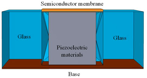
FIGURE 1. Schematic diagram of the sensor interior.
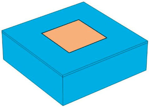
FIGURE 2. The overall appearance of the sensor model.
The sensor coupling system is composed of a piezoelectric-mechanical system and a piezoresistive system. The piezoelectric-mechanical system is in the electric field and mechanical strain. The inverse piezoelectric effect can be expressed as a matrix.
where x is the strain, d is the piezoelectric constant matrix, and E is the applied electric field strength matrix.
where x1 is the strain tensor, X1 is the stress tensor, S is the short-circuit elastic compliance constant, d31 is the free dielectric constant, and d31 is the voltage constant.
Changes in varistor resistance are caused by strain-induced changes in the material’s band structure and associated changes in carrier mobility and number density. The relationship between the electric field E and the current I in the varistor is:
where ρ is the resistivity and Δρ is the induced change in resistivity. In the general case, both ρ and Δρ are rank two tensors. The resistance change is related to the stress X, and the constitutive relationship between the two is:
where Π is the varistor tensor, which is a material property. If resistivity and stress are converted to vectors using simplified subscript notation, then it can be represented as a matrix.
The relationship between the internal electric field and current can also be expressed by a matrix as:
There is shear stress in a varistor, which is a result of the stress of the piezoelectric material in the semiconductor membrane. Through the piezoresistive effect, these shear stresses create an electric field or potential gradient in the varistor bridge arms transverse to the direction of the current flow. In the entire width of the varistor, the potential gradients are added together to generate an induced voltage difference between different bridge arms, and the electric field strength can be inferred from the magnitude of the generated voltage.
Based on the process theory of MEMS micro-sensors, the structure of the piezoelectric-piezoresistive coupled electric field measurement sensor is optimized. To obtain the optimal size of the sensor, the model design needs to meet:
1)The deformation of the piezoelectric material in the electric field is maximized;
2)The piezoresistive membrane can vibrate freely on the device;
3)The piezoelectric material is firmly coupled with the piezoresistive material.
Based on the above points, the conventional sensor parameters were selected, a sensor model with semiconductor membranes edge length of 500 μm, a thickness of 20 μm, piezoelectric material edge length of 350 μm and thickness of 300 μm is established.
The side length of the membrane is larger than the side length of the piezoelectric material so that the surrounding of the membrane is highly coupled with the glass and plays a fixed role. The glass layer has air pockets that provide enough space for the membrane to vibrate. The piezoelectric material is the same height as the glass, embedded in the glass layer, and the pyramid glass fixes the piezoelectric material. The substrate is made of glass, and is reliably fixed with the lower surface of the piezoelectric crystal so that the crystal is deformed along the positive direction of the z-axis, the strain is transmitted to the semiconductor membrane to the maximum extent, and the measurement accuracy of the sensor is improved. The X-Z planar structure of the sensor is shown in Figure 3.
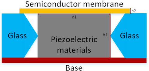
FIGURE 3. Schematic diagram of X-Z plane of sensor structure.
The sensor material parameters are shown in Table 1.
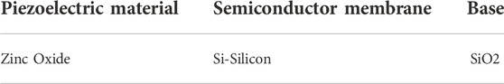
TABLE 1. Material settings of each part of the sensor.
The model sets the substrate, glass, and piezoelectric material as fixed constraints to ensure that the piezoelectric material deforms only in the positive direction of the z-axis. The ground terminal is the lower surface of the piezoelectric material, the voltage terminal is the upper surface of the piezoelectric material, and the voltage value is 1000 V.
The finite element method (FEM) was introduced by Comsol Multiphysics software to optimize the sensor structure.
To improve the calculation accuracy and calculation speed, the research objects are divided into piezoelectric materials, semiconductor membranes, glass, and substrates. The calculation grid is divided by free tetrahedrons. Since the main objects of size optimization are piezoelectric materials and semiconductor membranes, Therefore, more detailed mesh division is performed on piezoelectric materials and semiconductor membranes, as shown in Figure 4.
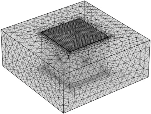
FIGURE 4. Meshing the sensor model.
The main optimization work of the sensor model is the optimization of semiconductor membrane and piezoelectric material. By using the method of control variable, the influence of the edge length and thickness of semiconductor membrane and piezoelectric material on the sensor performance is gradually explored to select the optimal parameters and complete the optimization of the sensor structure.
The side length of the piezoelectric material is studied by parametric scanning, starting from the side length of the piezoelectric material d1 = 350 μm, with a step size of 50 μm, and ending at d1 = 800 μm, the steady state study is carried out, the strain and displacement of piezoelectric materials with different side lengths in the steady electric field are obtained.
Analysis of Figure 5 and Figure 6 shows that the strain component and displacement increase from the center of the membrane at X = 0, reach a peak near the boundary of the piezoelectric material, and then decrease. The displacement peaks of piezoelectric materials with different side lengths differ slightly, but the strains vary greatly. In the material with side length less than 550μm, the strain peak of 400 μm side length is the highest, which is 6 × 10⁻⁵. Compared with the membrane with side length of 600μm–800μm, the strain is reduced by 15%–20%, but the side length is reduced. The piezoelectric material with a side length of 400 μm is selected to reduce the volume of the sensor based on ensuring the sensitivity of the sensor, and the strain performance is better, and it is also conducive to the miniaturization of the sensor design.
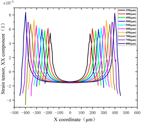
FIGURE 5. Strain situation of different semiconductor membranes.
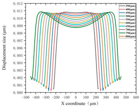
FIGURE 6. Displacement of semiconductor membranes at different d1.
Keep the side length of the piezoelectric material at 400μm, and change the thickness h1 of the piezoelectric material block to conduct steady-state research, starting from h1 = 200μm, with a step size of 50μm, and ending at h1 = 1000 μm. The strain and deformation results of piezoelectric materials with different thicknesses in steady electric field are obtained.
Analysis of Figure 7 and Figure 8 shows that as the thickness of the piezoelectric material increases, the piezoelectric effect becomes more obvious, the overall strain increases, but the distance between the cavities becomes shorter and the strain peak decreases. Therefore, both the strain amount and the maximum deformation displacement on the semiconductor membrane show a downward trend; the average strain amount increases first and then tends to be stable, and the displacement amount first increases and then decreases slowly. The piezoelectric thickness in the range of 300 ≤ h1 ≤ 400 material, the strain component is kept at a high 60 × 10–6, which is better than other piezoelectric materials. Considering the optimal strain and displacement factors, the piezoelectric material with thickness h1 = 350 μm is the best.

FIGURE 7. Strain induced on semiconductor membranes.
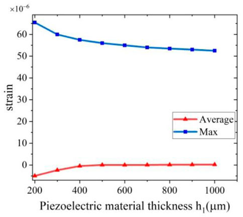
FIGURE 8. Displacement of the semiconductor membrane.
Keep the side length of the piezoelectric material as d1 = 400, the thickness of the piezoelectric material h1 = 350μm, change the thickness h2 of the semiconductor membrane, start from h2 = 5μm, step 5μm, and stop at h2 = 40μm, carry out steady-state research, and obtain different thicknesses strain and deformation results of semiconductor thin-membrane devices in steady-state electric fields.
Analysis of Figure 9 and Figure 10 shows that as the thickness of the semiconductor membrane increases, its strain sensitivity decreases, the maximum strain on the membrane first increases slowly and then decreases, the average value increases slowly, and the displacement decreases. When the membrane thickness is less than 15μm, the average value of the strain is negative. Therefore, when analyzing the semiconductor membrane with a thickness of 20μm–40μm, the maximum displacement and strain decrease with the increase of the membrane thickness, and the maximum strain peak of the 20 μm membrane is 60μm × 10–6, the smaller the thickness, the more obvious the strain, therefore, the semiconductor membrane with thickness h2 = 20 μm is the best.
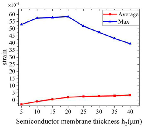
FIGURE 9. Strain of Semiconductor membranes of Different Thickness.
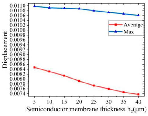
FIGURE 10. Displacement of semiconductor membranes of different thickness.
Based on the above results and combined with semiconductor membrane side length of the initial model, the piezoelectric material with side length d1 = 400μm, thickness h1 = 350μm, and semiconductor membrane with thickness h2 = 20 μm and side length d2 = 500 μm are used as the benchmark model to ensure the sensitivity of the sensor, and consider the design and processing, etc. Factors to meet the optimization needs of electric field measurement sensors.
After obtaining the optimized structural parameters of the sensor, the steady-state response simulation of the sensor structure is carried out on this model to test the performance of the sensor.
By analyzing the strain distribution of the sensor on the surface of the semiconductor membrane under the electric field of 1000V, it is obtained that the strain component σXX along the X axis is almost the same as the strain component σYY along the Y axis, so only σXX will be studied in the future, As shown in Figure 11.
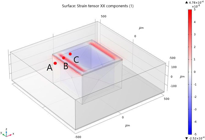
FIGURE 11. Surface strain distribution of semiconductor membranes, strain tensor: XX tensor.
According to previous research, the boundary between the semiconductor membrane and the piezoelectric material is the region with the largest strain, which is the optimal design position of the doped region. Since the strain distribution gradient near the boundary is large, and the positive and negative strains appear alternately, the selection of the appropriate ion doping region has a great impact on the sensor performance.
Through analysis, point A (-230, 0, 150), B (-220, 0, 150), and C (-210, 0, 150) are all located in the area with large boundary strain. Analysis of Figure 11 shows that points B and C are in the positive and negative strain change regions, and the sensitivity is low. Therefore, point A is studied. Figure 12A shows the strain tensor σXX of the membrane along the x-axis, and Figure 12B shows the strain tensor σXX of the membrane along the y-axis. Two regions A and B are taken in Figure 11, corresponding to the regions A and B in Figure 12, and the point A’ is the zero point of the strain tensor σXX at A and B.
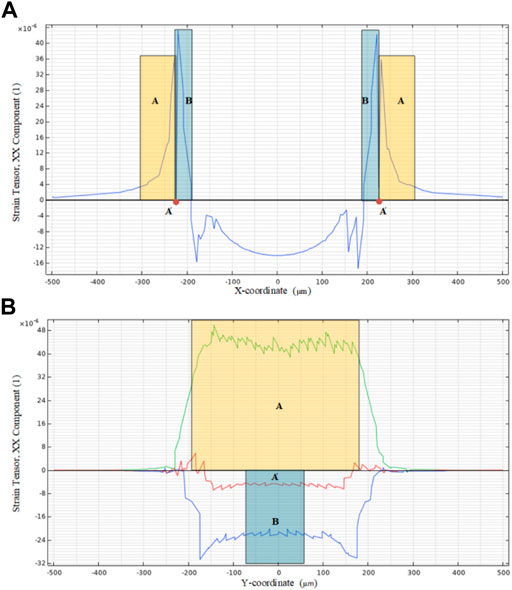
FIGURE 12. Strain tensors along the X-axis (A) and along the Y-axis (B).
Ax is obtained by integrating the strain tensor in the yellow part of Figure 12A and the area enclosed by σXX = 0, and Ay is obtained by integrating the strain tensor in the yellow area in Figure 12B and the area enclosed by σXX = 0, where Ax and Ay are doping area strain tensor. The strain tensors in the blue area are processed in the same way to obtain Bx and By as the strain tensors of the B area. By comparing the integral area, the strain tensor at A is significantly larger than that at B. Therefore, in a comprehensive analysis, the position of A is the best area for ion doping.
After the semiconductor doping area is determined, a piezo resistor patch is placed on the thin membrane of the above-mentioned benchmark model, so that the model has a bridge structure for outputting electrical signals, as shown in the gray part of Figure 13.
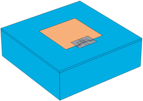
FIGURE 13. Piezoresistive patch setting position (gray part).
Set the X bridge of the varistor at the place where the semiconductor membrane has the greatest strain. As shown in Figure 14, set a 3 V voltage on the upper left arm of the X bridge, and connect the lower right arm to the ground. In the electric field, the piezoelectric material induces deformation, which drives the semiconductor membrane to apply shear stress on the varistor, making the potential distribution uneven, and the bridge arm will generate an induced voltage difference, as shown in Figure 15.
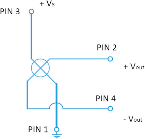
FIGURE 14. Piezoresistive patch Schematic.
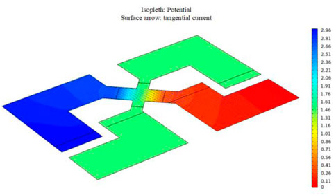
FIGURE 15. Current density and potential distribution of varistor under pressure.
When testing the performance indicators of the electric field sensor, it needs to be carried out in a quantifiable uniform electric field environment. Test methods and platforms for traditional electric field sensors are usually based on a uniform electric field formed by standard parallel metal plates. According to the principle of parallel plate electric field: ideally, a stable voltage of different amplitudes can be loaded on two parallel plate electrodes of infinite size and a certain distance, and a uniform electric field can be formed between the parallel plates, and the electric field direction is perpendicular to the two parallel plates, and the electric field strength can be calculated from Equation 7.
Here, E is the electric field strength of the sensor; U is the difference in DC voltage applied across the sensor; d is the sensor height. The electric field sensor is placed in the middle of the parallel plate electric field device, the voltage applied to both ends of the sensor is changed, the electric field strength E is generated, and the output amount of the electric field sensor is recorded, so that the relationship between the input electric field strength E and Uout can be determined, and the input and output characteristics of the electric field sensor can be obtained.
In Table 2, V1 is the voltage applied to the upper end of the piezoelectric material. In the range of 0 V ∼ -1000V, the electric field strength is 0–2.86 × 10⁻⁶V/m.
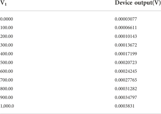
TABLE 2. Working current and output voltage of varistor driven by 3 V applied voltage.
Analysis of Figure 16 shows that the electric field where the piezoelectric material is located is different, and the voltage value output by the patch is also different. The output voltage of the patch has a linear relationship with the applied voltage of the piezoelectric material. Therefore, the electric field intensity of the sensor can be obtained by the voltage signal output from the piezoresistive patch.

FIGURE 16. The output voltage value of the varistor under the driving of the applied voltage.
In this paper, a MEMS electric field measurement sensor model based on the piezoelectric-piezoresistive coupling is constructed by the finite element method, and the steady-state characteristics of the micro electric field sensor under different sizes of piezoelectric materials and semiconductor membranes are simulated and analyzed, and the following conclusions are obtained:
As the side length of the piezoelectric material increases, the difference in peak displacement between different side lengths of the piezoelectric material is small, but the difference in the amount of strain is large. The strain component and the amount of displacement increase from the center of the membrane, and reach the peak value near the piezoelectric material boundary.
As the thickness of the piezoelectric material increases, the piezoelectric effect is more obvious, and the overall strain amount increases, but the distance between the cavities becomes shorter and the strain peak decreases. Therefore, both the strain amount and the maximum deformation displacement on the semiconductor membrane show a downward trend; the average strain amount first increases and then tends to be stable, and the displacement amount first increases and then decreases slowly.
As the thickness of the semiconductor membrane increases, its strain sensitivity decreases. The maximum strain on the membrane first increases slowly and then decreases, the average value is in a slow increasing trend, and the displacements all show a decreasing trend.
The piezoelectric material with side length d1 = 400 μm, thickness h1 = 350 μm, semiconductor membrane thickness h2 = 20 μm, semiconductor side length d2 = 500 μm has high sensitivity, and meets the design requirements for electric field measurement.
By studying the strain on the surface of the membrane, the optimal doping area for placing the varistor patch was designed. Tests the output characteristics of the sensor in a uniform electric field of 0–2.86 × 10⁻⁶ V/m, thus verifying the feasibility of the sensor in electric field measurement.
The original contributions presented in the study are included in the article/Supplementary Material, further inquiries can be directed to the corresponding author.
GL guided the experimental simulation. YY is responsible for writing the paper. Other provided some guidance.
BL was employed by China Southern Power Grid Technology Research Institute Co., Ltd. YG was employed by China Southern Power Grid Co. Ltd EHV Transmission Company Guangzhou Bureau. SC was employed by Guangdong Shuangdian Technology Co., Ltd
The remaining authors declare that the research was conducted in the absence of any commercial or financial relationships that could be construed as a potential conflict of interest.
All claims expressed in this article are solely those of the authors and do not necessarily represent those of their affiliated organizations, or those of the publisher, the editors and the reviewers. Any product that may be evaluated in this article, or claim that may be made by its manufacturer, is not guaranteed or endorsed by the publisher.
Ando, B., Baglio, S., Savalli, N., and Trigona, C. (2011). Cascaded “triple-bent-beam” MEMS sensor for contactless temperature measurements in nonaccessible environments. IEEE Trans. Instrum. Meas. 60 (4), 1348–1357. doi:10.1109/tim.2010.2101310
Aristizabal-Tique, V. H., Gómez-Montoya, N. A., Salazar-Escobar, H., Velez-Hoyos, F. J., and Florez-Velasquez, C. A. (2020). Performance parameters estimation of Pockels high-voltage sensors by means of numerical optimization. IEEE Trans. Instrum. Meas. 69 (4), 1540–1546. doi:10.1109/tim.2019.2912590
Chen, W., Li, B., and Huang, J. (2016). A CMOS MEMS humidity sensor enhanced by a capacitive coupling structure. Micromachines 7 (5), 74. doi:10.3390/mi7050074
Cui, Y., Yuan, H., Song, X., Zhao, L., Liu, Y., and Lin, L. (2017). Model, design, and testing of field mill sensors for measuring electric fields under high-voltage direct-current power lines. IEEE Trans. Ind. Electron. 65 (1), 608–615. doi:10.1109/tie.2017.2719618
Frantlovic, M., Jokic, I., Lazic, Z., Smiljanic, M., Obradov, M., Vukelic, B., et al. (2016). A method enabling simultaneous pressure and temperature measurement using a single piezoresistive MEMS pressure sensor. Meas. Sci. Technol. 27 (12), 125101. doi:10.1088/0957-0233/27/12/125101
Iqbal, F., and Lee, B. (2018). “Measurement uncertainties in electrostatic actuated MEMS resonators[C],” in Symposium on Design,Test,Integration & Packaging of MEMS and MOEMS, Italy, May 22–May 25, 2018.
Kainz, A., Steiner, H., Schalko, J., Jachimowicz, A., Kohl, F., Stifter, M., et al. (2018). Distortion-free measurement of electric field strength with a MEMS sensor. Nat. Electron. 1 (1), 68–73. doi:10.1038/s41928-017-0009-5
Liu, L., Li, X., Wen, T., Zhang, R., Wu, Z., Zhao, J., et al. (2019). Investigation on surface electric field distribution features related to insulator flashover in SF6 gas. IEEE Trans. Dielectr. Electr. Insul. 26 (5), 1588–1595. doi:10.1109/tdei.2019.008194
Liu, L., Li, X., Zhang, Q., Liang, C., Ren, H., Zhao, J., et al. (2018). The influence of electric field distribution on insulator surface flashover[C],” in IEEE Conference on Electrical Insulation and Dielectric Phenomena, Cancun, Mexico, October 21–October 24, 2018
Nag, M., Singh, J., Kumar, A., and Singh, K. (2020). A high sensitive graphene piezoresistive MEMS pressure sensor by integration of rod beams in silicon diaphragm for low pressure measurement application. Microsyst. Technol. 26 (9), 2971–2976. doi:10.1007/s00542-020-04890-x
Qi, B., Zhao, X., and Li, C. (2016). Methods to reduce errors for DC electric field measurement in oil-pressboard insulation based on Kerr-effect. IEEE Trans. Dielectr. Electr. Insul. 23 (3), 1675–1682. doi:10.1109/tdei.2016.005507
Sahay, R., and Jindal, S. K. (2021). Design and analysis of a MEMS pressure sensor with a bossed membrane and ancillary bi-functional frog arm structure for low pressure measurement. J. Comput. Electron. 20 (2), 1012–1019. doi:10.1007/s10825-021-01660-4
Shanhong, X., Hucheng, L., Jun, Liu., Chu, , et al. (2021). Research and development on MEMS based electric field sensor[C]//International conference on solid-state sensors. Actuators Microsystems 12 (7).
Torunbalci, M. M., Alper, S. E., and Akin, T. (2015). “The advanced MEMS process for fabricating wafer level vacuum packaged SOI-MEMS devices with embedded vertical feedthroughs[C],” in 2015 Transducers – 2015 18th International Conference on Solid-State Sensors,Actuators and, Alaska, USA, June 21–June 25, 2015.
Wang, J., Wu, H., Deng, Z., Peng, Z., and Liao, J. (2015). E-field distribution analysis on three types of converter double valve in 800kV valve hall[C],” in 2015 IEEE 11th International Conference on the Properties and applications of Dielectric Materials, Australia, July 19–July 22, 2015
Wu, H., Li, C., Qi, B., Zhao, X., Li, J., and Zhao, L. (2012). The electric field distribution in oil-paper insulation under combined AC-DC voltage[C],” in 2012 IEEE International Conference on Condition Monitoring and Diagnosis, Bali, Indonesia, September 23–September 27, 2012
Yang, Q., Sun, S., Han, R., Sima, W., and Liu, T. (2015). Intense transient electric field sensor based on the electro-optic effect of LiNbO3. AIP Adv. 5 (10), 107130. doi:10.1063/1.4934720
Yong, C., Haiwen, Y., Xiao, S., Luxing, Z., Yumeng, L., and Liwei, L. (2018). Model, design, and testing of field mill sensors for measuring electric fields under high-voltage direct-current power lines[J]. Industrial Electron. IEEE Trans.65 (1), 608.
Zeng, R., Zhuang, C., Niu, B., Yu, Z., and He, J. (2013). Measurement of transient electric fields in air gap discharge with an integrated electro-optic sensor. IEEE Trans. Plasma Sci. IEEE Nucl. Plasma Sci. Soc. 41 (4), 955–960. doi:10.1109/tps.2013.2249669
Zhang, J., Lu, T., Zhang, W., Zhang, X., and Hu, Y. (2019). Calculation of RFI from valve hall in MMC-HVDC converter station. Int. J. Appl. Electromagn. Mech. 59 (1), 27–37. doi:10.3233/jae-171230
Keywords: electric field measurement, MEMS sensor, finite element simulation, piezoelectric effect, piezoresistive effect
Citation: Liu G, Ye Y, Luo B, Gu Y, Zheng W and Chen S (2023) Structural optimization and simulation of piezoelectric- piezoresistive coupled MEMS steady-state electric field sensor. Front. Energy Res. 10:1006777. doi: 10.3389/fenrg.2022.1006777
Received: 29 July 2022; Accepted: 31 October 2022;
Published: 13 January 2023.
Edited by:
Peng Li, Tianjin University, ChinaReviewed by:
Narottam Das, Central Queensland University, AustraliaCopyright © 2023 Liu, Ye, Luo, Gu, Zheng and Chen. This is an open-access article distributed under the terms of the Creative Commons Attribution License (CC BY). The use, distribution or reproduction in other forums is permitted, provided the original author(s) and the copyright owner(s) are credited and that the original publication in this journal is cited, in accordance with accepted academic practice. No use, distribution or reproduction is permitted which does not comply with these terms.
*Correspondence: Yuanhao Ye, MTA1NTA1MTMwNUBxcS5jb20=
Disclaimer: All claims expressed in this article are solely those of the authors and do not necessarily represent those of their affiliated organizations, or those of the publisher, the editors and the reviewers. Any product that may be evaluated in this article or claim that may be made by its manufacturer is not guaranteed or endorsed by the publisher.
Research integrity at Frontiers
Learn more about the work of our research integrity team to safeguard the quality of each article we publish.