 Xiaoyue Chen
 Zeyu He
 Yanze Zhang
 Junjie Si
 Shuang Wang
 Baoquan Wan3
- 1School of Electrical Engineering and Automation, Wuhan University, Wuhan, China
- 2State Grid Shaoxing Power Supply Company, Shaoxing, China
- 3State Key Laboratory of Power Grid Environmental Protection, Wuhan, China
The disconnector switching operation in GIS not only generates very fast transient overvoltage (VFTO) in primary equipment, but also couples to the secondary system, which affects normal operation of the secondary equipment. In this study, aiming at the conducted disturbance caused by the disconnector switching operation of the 1,000-kV UHV GIS test circuit on the secondary cable, a broadband equivalent circuit model of the potential transformer and the grounding grid is proposed based on the vector fitting method and the impedance synthesis method, and the accuracy of the model is tested. On the basis of this model, the conducted disturbance voltage of the secondary cable core is obtained by combining the measured typical disturbance source waveform. The research results of the influencing factors of conducted disturbance show that the amplitude of the disturbance voltage generated by the capacitive conduction is higher than that generated by the resistive conduction, but the main frequency of the resistive conducted disturbance voltage is higher. The amplitude of the conducted disturbance voltage will decrease with the increase of the length of the cable and the length of the grounding wire. The single-ended grounding of the secondary cable shield at the GIS side will cause serious disturbance voltage. The research results of this study will be beneficial to the protection of secondary cable electromagnetic disturbance in the intelligent substation and have reference significance for the implementation of secondary equipment protection measures in the intelligent substation.
Introduction
Gas insulated switchgear (GIS) is widely used in substations due to its high reliability and small footprint. However, very fast transient overvoltage (VFTO) and transient enclosure voltage (TEV) appear when switching in GIS. Simulation and experiment show that the rise time of VFTO is only nanosecond grade, the frequency range mainly includes several to dozens of MHz, up to 100 MHz, and the amplitude range is generally between 1.5 p.u. and 2.8 p.u. The peak value of TEV can reach tens of kV, and it has higher frequency components than VFTO. In the development of a smart grid, there are new requirements for power system protection and control (Bo et al., 2016; Zhang et al., 2016). At present, intelligent equipment is widely used in the power system, especially in relay protection (Nan et al., 2018; Yang et al., 2021). The intelligent equipment on the secondary side is vulnerable to electromagnetic disturbance, and the cable is the key to the transmission of electromagnetic disturbance to the intelligent equipment.
High-frequency and high-amplitude VFTO and TEV not only pose a threat to the insulation of GIS and winding equipment such as transformers and reactors connected to it, but also interfere with the normal operation of secondary equipment in a substation (D’Souza et al., 2020; Moreira et al., 2020). The VFTO and TEV transmitted in the primary equipment will be coupled to the secondary circuit through conduction and radiation. The disturbance voltage is generated on the secondary cable core, which will interfere with the sensitive secondary equipment of the cable terminal and may cause its misoperation. However, since the conducted disturbance in a substation is far more significant than the radiated disturbance, the radiated disturbance can be ignored when calculating the disturbance voltage of the secondary cable (Mahmood et al., 2015).
Some scholars have carried out corresponding research on the problem of electromagnetic disturbance source disturbing secondary equipment when operating a disconnector. The research methods mainly include field test, laboratory test, and numerical calculation (Cai et al., 2018). At the beginning of the 21st century, China has built a large number of GIS substations. In order to explain the mechanism and influencing factors of electromagnetic disturbance caused by disconnector switching operation, the China Electric Power Research Institute has combined several universities to build two disconnector test platforms with different operating speeds at the UHV AC test base of State Grid Corporation in Wuhan. The electromagnetic disturbance caused by the disconnector switching operation in GIS was systematically studied, and a large number of experimental measurement data were obtained (Chen et al., 2011; Zhang et al., 2013; Zhang et al., 2014; Hu et al., 2015; Ma et al., 2017).
Due to the complexity of field measurement and laboratory test method, the numerical calculation method has been widely used. In 1988, CIGRE Working Group 33/13.09 proposed in detail the equivalent circuit models of the main components of GIS equipment such as GIS bus, disconnector, circuit breaker, insulator, and bushing, but these models are only applicable to the calculation of internal transient field at low frequency, without considering the high-frequency response of components (CIGRE Working Group 33/13.09, 1988). Jiao et al. (2016) decomposed the specific structure of bushing into multiple parts, extracted and combined the parameters of different parts, and established the broadband equivalent circuit model of high voltage bushing. The model was in good agreement with the full-wave simulation results. Feng et al. (2014) modeled the specific structure of each component by HFSS (High Frequency Structure Simulator), obtained the parasitic parameters, and constructed the calculation model of conducted disturbance in the GIS substation. The simulation results are consistent with the experimental data. Hu (2016) uses the “black box method” to establish the high-frequency transmission function model of each component and establishes the broadband equivalent circuit model of grounding grid and grounding pillar by vector fitting method and impedance synthesis method, and embeds the data into EMTP to realize the calculation. In Wang and Yang (2016), the high-order Radau method is proposed to simulate the electromagnetic transient (EMT) of the power system. The corresponding high-dimensional linear algebraic equations are decoupled into blocks in time domain, and a multi-stage block recursive method is formed. This method avoids the numerical oscillation in calculation and has achieved good results in VFTO calculation of the 550-kV GIS system.
In summary, a large number of simulation studies have been carried out on the electromagnetic disturbance of the secondary cable caused by disconnector switching operation. However, most of the simulation uses a single numerical lumped parameter to model the components, which cannot reflect the broadband response characteristics of the components. In view of the above problems, this study deeply studies the establishment method of the broadband equivalent circuit model of each component in the simulation analysis of electromagnetic disturbance. The level and influencing factors of conducted disturbance voltage produced by the disconnector switching operation of the secondary cable are analyzed by simulation analysis, and the electromagnetic disturbance suppression measures of secondary cable are proposed. The research results of this study will be beneficial to the reasonable arrangement of secondary cables in the intelligent substation and have reference significance for the implementation of secondary equipment protection measures in the intelligent substation.
Coupling Mechanism of Conducted Disturbance
In terms of the disturbance path, the electromagnetic disturbance caused by GIS disconnector switching operation to the secondary cable is mainly divided into conducted disturbance and radiated disturbance. However, usually the conducted disturbance in a substation far exceeds the radiated disturbance, so the radiated disturbance is often ignored when calculating the disturbance voltage of the secondary cable. The secondary equipment in a substation has low sensitivity to power frequency disturbance, but it has high sensitivity to high-frequency disturbance component, so it is prone to failure or damage under the high-frequency electromagnetic disturbance generated by disconnector switching operation.
Conducted disturbance refers to that in two circuits with electrical connection; the electrical signal (disturbance voltage or current) of one circuit is transmitted to another circuit through the common circuit, which is mainly divided into capacitive conduction and resistive conduction.
Capacitive conduction refers to the electromagnetic transient process in which the VFTO generated by the disconnector switching operation in the GIS bus is directly coupled to the core of secondary cable through stray capacitance between primary winding and secondary winding of a potential transformer. Due to the different response characteristics of the transformer port in case of high frequency, the modeling method using a single numerical lumped element to describe the transformer will inevitably cause errors, so it is necessary to establish the broadband equivalent circuit model of the transformer.
Resistive conduction means that TEV generated by disconnector switching operation propagates along the enclosure in the form of a voltage wave. When it propagates to the grounding point of GIS enclosure, part of the voltage wave will couple to the grounding wire, and flow into the grounding grid along the grounding wire, causing the grounding grid potential to rise. Generally, the shield layer of the secondary cable is grounded at both ends. Therefore, under the effect of TEV, the potential of the shield layer of the secondary cable increases and the shielding effect decreases, and the voltage will be generated between the two grounding points, which will generate transient current on the shield layer of the secondary cable, and then couple to the core wire to generate disturbance voltage.
To sum up, capacitive conduction and resistive conduction are closely related to the potential transformer and grounding grid. The simple lumped element modeling cannot reflect its response characteristics in high frequency, and it will cause considerable errors under the excitation of VFTO and TEV disturbance sources with complex frequency components. Therefore, in order to ensure the accuracy of calculation, the broadband equivalent circuit model of the potential transformer and grounding grid should be established in the simulation of conducted disturbance caused by disconnector switching operation.
Establishment of Broadband Equivalent Circuit Model
The Method of Modeling
The establishment of an equivalent circuit model can be generally divided into two methods: traditional equivalent circuit model and black box model. The traditional equivalent circuit model uses analytical formulas or simulation software to solve complex electromagnetic field problems based on physical factors such as the concrete structure and material of components. Every equivalent circuit element obtained by this method has actual physical meaning. The model meaning is intuitive, but it is necessary to know the detailed physical structure of each component, and the modeling and solving are more complex.
The black box model does not focus on the specific structure of the component to be tested, but obtains the frequency response of the component through actual measurement or simulation, and then determines the circuit expression of the element according to the numerical fitting method. The disadvantage of this method is that each component in the circuit model has no specific significance, but it avoids the complex electromagnetic field problem when using the traditional equivalent circuit model, and does not need to know the specific structure of each component.
In this study, the black box model is used to establish the broadband equivalent circuit model of the potential transformer and grounding grid. The specific method is used to obtain the broadband response characteristics of the potential transformer and grounding grid. Then, the stable and effective vector fitting method is used to fit the broadband response characteristics and the rational function expressions of the broadband response characteristics of the potential transformer and grounding grid are obtained. Finally, based on the analysis of the relationship between the time domain model and the complex frequency domain function, the broadband equivalent circuit model of the transformer and grounding grid is obtained.
Method of Establishing Broadband Equivalent Circuit
Based on the broadband response characteristics of the component, it can be assumed that its rational function expression is of the form of Eq. 1 (Gustavsen and Semlyen, 1998; Deschrijver et al., 2008):
Where n is the order of the pole, and an, cn, d, and h are the unknowns in the expression, which are the poles, residue, constant term, and coefficient of first order term, respectively. These unknowns can be fitted by vector fitting method.
It is assumed that there are K pairs of conjugate complex poles after rational fitting of broadband response by vector fitting method, and the nth pair of conjugate complex poles is expressed as:
Where n = 1,2,…,k, and prn is the real part of the conjugate complex poles, and prn >0. It is assumed that the residue corresponding to the pair of complex poles:
Combining Eq. 2 and Eq. 3, Eq. 1 can be divided into the following three parts:
If f(s) is the expression of impedance, the above three parts can be represented by the circuit form in Figure 1.
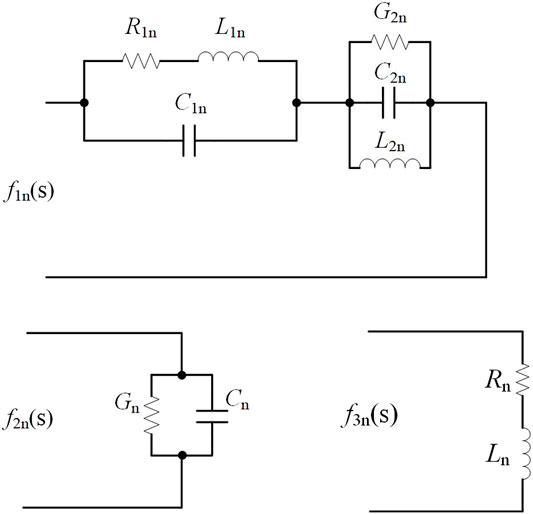
FIGURE 1. Circuit forms of expression.
The elements in the circuit are obtained according to the following formula:
The final broadband equivalent circuit model can be established by connecting the above three parts in series.
If f(s) is the expression of admittance, the corresponding broadband equivalent circuit can be established by parallel connection in the same way.
Broadband Equivalent Circuit of Grounding Grid
This study takes the grounding grid of GIS test circuit at the UHV AC test base in Wuhan as the research object. The cable layout is shown in Figure 2, and the actual geometry of the ground grid is shown in Figure 3. The size of each grid is 0.8 m × 0.8 m, and the size of the small grid is 0.4 m × 0.4 m. It is assumed that the two conductors of the vertical grounding grid are the two grounding wires of the secondary cable shield layer. The grounding grid is set up with steel material, and the relative resistivity ρr is 10, relative permeability μr is 626 (relative to copper), the buried depth of ground grid is 0.8 m, and the conductor radius is 8 mm. Soil modeling is divided into two layers: the top soil resistivity is 28.43 Ω m and the thickness is 39.94 m; the bottom soil resistivity is 240,302 Ω m and the thickness is infinite.
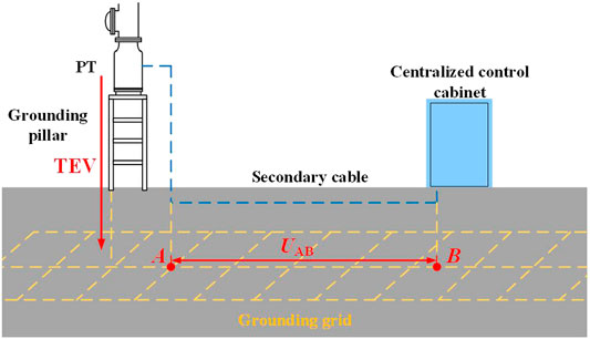
FIGURE 2. The cable layout.
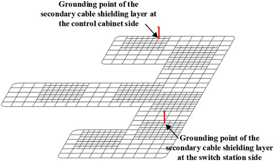
FIGURE 3. Grounding grid structure.
By injecting current of different frequencies into the grounding point and measuring the response of each grounding point, the T-shaped two port equivalent circuit of the whole grounding grid can be established, as shown in Figure 4A.
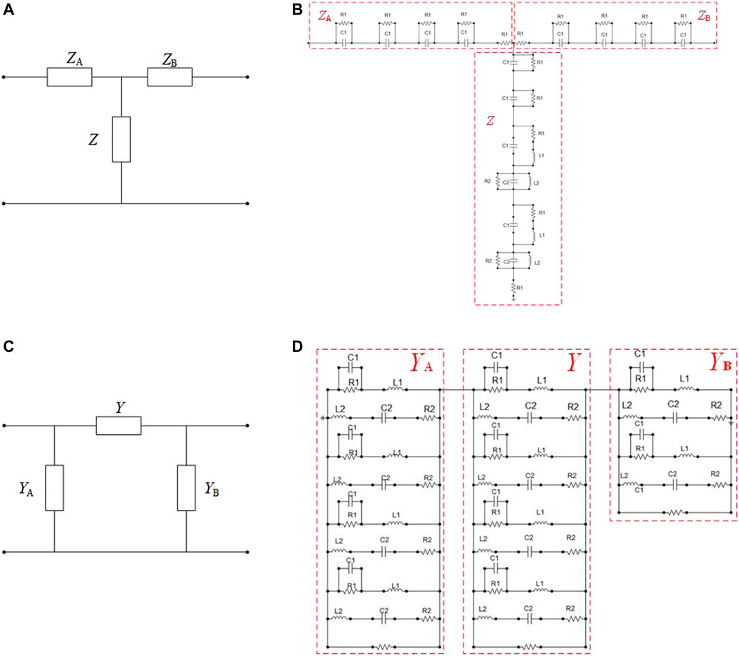
FIGURE 4. Two port equivalent circuit. (A) T-shaped two port equivalent circuit; (B) The broadband equivalent circuit model of grounding grid; (C) π-shaped network of potential transformer. (D) The broadband equivalent circuit model of potential transformer.
Through the comparison of fitting effects of different pole orders, ZA, Z, and ZB are fitted with 4, 6, and 4 poles, respectively, and the fitting results are shown in Figure 5.
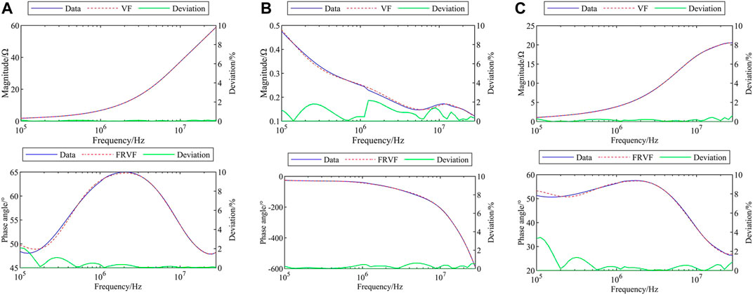
FIGURE 5. Fitting results of grounding grid model. (A) Fitting results of ZA. (B) Fitting results of Z. (C) Fitting results of ZB.
It can be seen from Figure 5 that the error of the amplitude-frequency and phase-frequency errors of the results fitted by vector fitting method is less than 5%, which can meet the needs of calculation accuracy. The results of vector fitting are implemented in the circuit in Figure 1, and the overall broadband equivalent circuit model of the grounding grid can be established. The circuit model of the grounding grid is shown in Figure 4B.
Broadband Equivalent Circuit of a Potential Transformer
In this study, the simulation model of a potential transformer is established by using the measured S parameter matrix of broadband response of the potential transformer in Wang (2010). The measured S parameter matrix is converted into an admittance matrix, and the two-port equivalent π-shaped network of the potential transformer is shown in Figure 4C.
The broadband characteristics of each admittance in the circuit can be rationally fitted by the same method. According to the rational function, the broadband equivalent circuit model of the potential transformer can be established by the same method, as shown in Figure 4D.
Simulation of Conducted Disturbance Caused by Disconnector Switching Operation
Research Objects
In this study, the GIS test circuit of the UHV AC test base (hereinafter referred to as the test circuit) shown in Figure 6 is taken as the research object. The thickened real line represents the GIS bus, and the virtual line represents the secondary cable. DS and ES represent the disconnector and grounding switch in GIS, respectively.
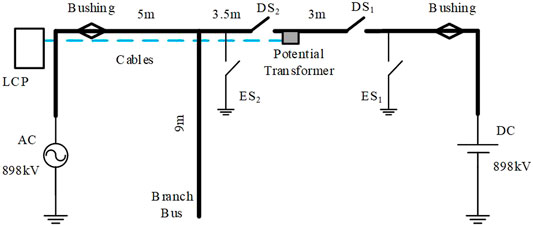
FIGURE 6. UHV GIS test circuit.
The research team led by the China Electric Power Research Institute has conducted thousands of closing and opening tests of disconnectors in the test circuit, and obtained a large number of VFTO, TEV, and space electromagnetic field test data. Therefore, this study considers using the measured data of the test as the excitation to join the simulation model to calculate the disturbance voltage. The typical measurement waveforms of VFTO, TEV, and spatial electromagnetic field provided by the above research team in Chen et al. (2011) and Hu et al. (2015) are selected as the excitation sources of this study, and the waveform of the disturbance source is shown in Figure 7.
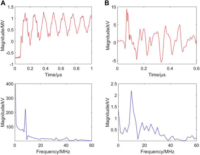
FIGURE 7. Typical measured disturbance source waveform. (A) VFTO. (B) TEV.
Simulation of Conducted Disturbance
KVVP2-22 quad cable is selected as the research object. In the modeling process, the J.Marti model suitable for the frequency conversion problem is used, and the corresponding simulation model is established combined with the geometric structure of the secondary cable.
The simulation model of conducted disturbance can be built in EMTP/ATP electromagnetic transient simulation software, as shown in Figure 8. Because the secondary cable shield layer is connected with the GIS enclosure in the GIS test circuit, the disturbance source TEV is directly loaded on the grounding point at the side of the GIS test circuit in the resistive conducted disturbance. In Figure 8, ZL1 and ZL2 represent the impedance of the grounding wire of the secondary cable shield layer. The terminal impedance R of core wire is 50 Ω.
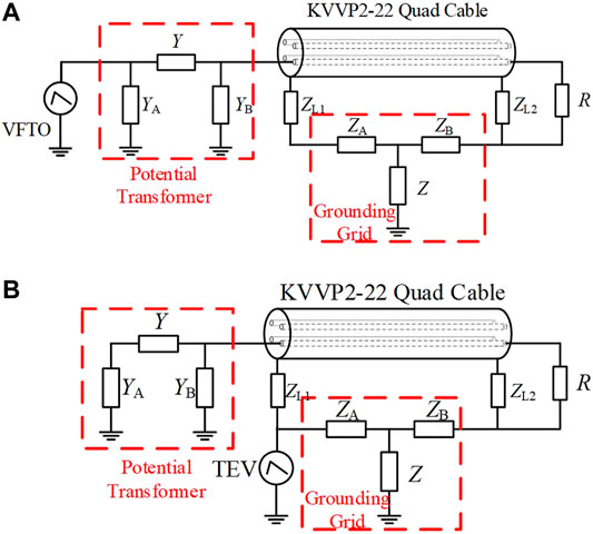
FIGURE 8. Simulation diagram of conducted disturbance. (A) Calculation model of capacitive conducted disturbance voltage. (B) Calculation model of resistive conducted disturbance voltage.
The cable length is set to 20 m, the shield layer is grounded at both ends, the simulation step length is set to 0.5 ns, and the total calculation time is 0.6 μs. In 0.6 µs, the maximum amplitude of the disturbance source has passed, and the waveform has begun to decay, so it can meet the most serious conducted disturbance level in the whole disturbance process. By measuring the potential difference between the two ends of the load, the conducted disturbance voltage level under the action of typical disturbance sources can be obtained. The disturbance voltage level of the secondary cable core under the excitation of typical disturbance source is shown in Figure 9.
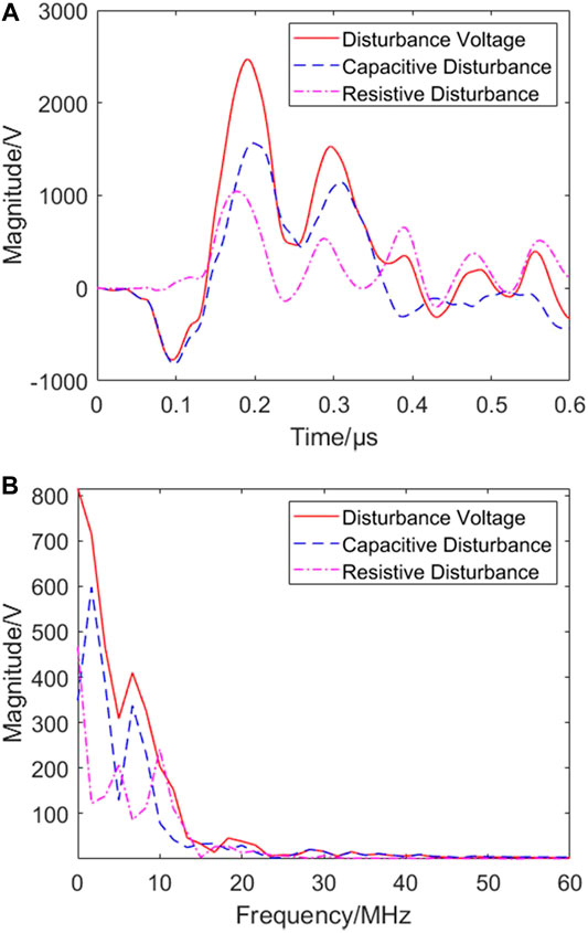
FIGURE 9. Conducted disturbance voltage of secondary cable. (A) Time domain waveform. (B) Spectrogram.
The calculation results show that under the excitation of typical disturbance source, the overall conducted disturbance voltage amplitude of the test circuit is about 2.5 kV, in which the capacitive conducted disturbance amplitude is about 1.5 kV, and the resistive conducted disturbance voltage amplitude is about 1.0 kV. From the perspective of frequency characteristics, the main frequency of the overall disturbance voltage is 6.7 MHz and below 5 MHz, and the main frequency of resistive conducted disturbance is higher than that of capacitive conducted disturbance. It can be seen that the capacitive transmission accounts for the main component in the conducted disturbance, accounting for 64% (Proportion of each disturbance voltage = Voltage area corresponding to each disturbance path/Total disturbance voltage area × 100%).
Analysis of Factors Affecting Conducted Disturbance
Cable Length
The disturbance voltage of the secondary cable also has high-frequency characteristics, so the propagation in the secondary cable needs to be considered by traveling wave. When the disturbance voltage wave propagates to both ends of the cable, the refraction and reflection will occur. The superposition of traveling waves may produce higher amplitude overvoltage, and the cable length directly affects the times of refraction and reflection in the whole transient process. In order to study the influence of cable length on the conducted disturbance voltage, the length L of cable is changed to 10, 20, 30, and 50 m, respectively. The time-domain waveform and frequency spectrum of terminal disturbance voltage under different cable lengths are calculated, as shown in Figure 10.
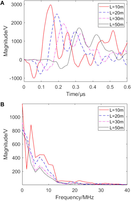
FIGURE 10. Conducted disturbance voltage of secondary cable. (A) Time domain waveform. (B) Spectrogram.
Figure 10 shows that with the increase of cable length, the disturbance voltage amplitude of the secondary cable core shows a downward trend. This is because when the cable length is short, the voltage wave will undergo multiple refraction and reflection in the propagation process. The continuous superposition of the incident wave and the reflected wave increases the disturbance voltage and has more high-frequency components. However, when the cable length is long, the number of refraction and reflection of voltage wave decreases significantly and attenuates continuously in the propagation process, so the amplitude decreases and the high-frequency component decreases significantly.
Grounding Mode of Shield Layer
At present, it is generally recognized that shielded cables are used in GIS substations in the world. However, there are different opinions on the grounding mode of the secondary cable shield layer. IEEE believes that shielded cables should be grounded at one end (IEEE Std 1143™-2012, 2012), while IEC and State Grid believe that shielded cables should be grounded at both ends (IEC 61000, 1997). Therefore, this section studies the influence of three different grounding modes on conducted disturbance, including two-end grounding of the shield layer, single-end grounding of the GIS side, and single-end grounding of the control cabinet side. The calculation results are shown in Figure 11.
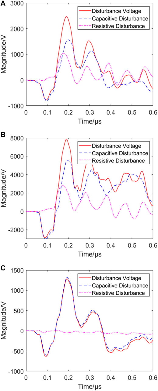
FIGURE 11. Conducted disturbance voltage of secondary cable. (A) Two ends grounding. (B) Grounding of GIS side. (C) Grounding of control cabinet side.
The calculation results show that the shield layer grounding mode has a great influence on the conducted disturbance, especially for the resistive conduction component. When the secondary cable shield layer is only grounded at the GIS side, the disturbance voltage is the most serious, and the amplitude is nearly 8 kV, which will seriously endanger the normal operation of the secondary equipment. When the shield layer is only grounded at the single end of the control cabinet side, the disturbance voltage level is the lowest, and the amplitude is only 1.3 kV. The reason is that TEV will lead to the increase of grounding grid potential. When the shield layer is grounded at the single end of the control cabinet, the grounding potential is low due to the distance from the GIS grounding wire, so it plays a good shielding effect on the core wire, and the resistive conduction component is in a very small value. When the shield layer is grounded at the single end of the GIS, due to the point close to the GIS grounding wire, the TEV will flow into the grid, and have a high potential. At this time, the whole shield layer will be in a high potential state, resulting in poor shielding effect of the cable and serious disturbance voltage on the core line.
Length of Grounding Wire
The grounding wire of secondary cable is usually inductive, and the voltage drop cannot be ignored when the high-frequency current flows. Table 1 shows the level of conducted disturbance voltage when the grounding wire length is 1, 1.5, 2, and 2.5 m, respectively.
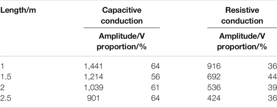
TABLE 1. Influence of grounding wire length on disturbance voltage.
The calculation results show that the disturbance voltage level on the secondary cable will decrease with the increase of the length of the grounding wire. The reason is that the impedance of the grounding wire increases with the increase of the length of the grounding wire. When the resistive conduction source TEV is constant, the increase of the length of the grounding down lead will increase ZL1 and ZL2 in Figure 8B. Therefore, the partial voltage on the cable shielding layer decreases, the shunt of the grounding grid increases, the transient current on the shielding layer decreases, and the conducted disturbance voltage decreases.
Figure 12 shows the relationship between the voltage difference at the grounding point of the secondary cable shield layer and the transient current amplitude of the shield layer flowing through the grounding line length, which also proves the analysis in this study.
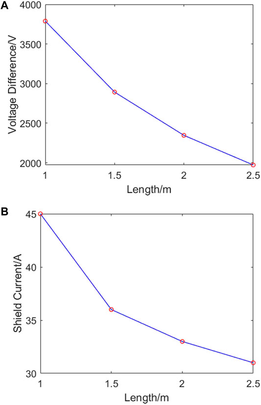
FIGURE 12. Voltage and shield current of shield layer. (A) Voltage of shield layer. (B) Shield current of shield layer.
Terminal Impedance of Secondary Equipment
The terminal impedance of secondary equipment is usually 50 Ω or 100 Ω. The calculation results of the terminal impedance of 50 Ω are given in the preceding section, and the calculation results of the terminal impedance of 100 Ω are shown in Figure 13.
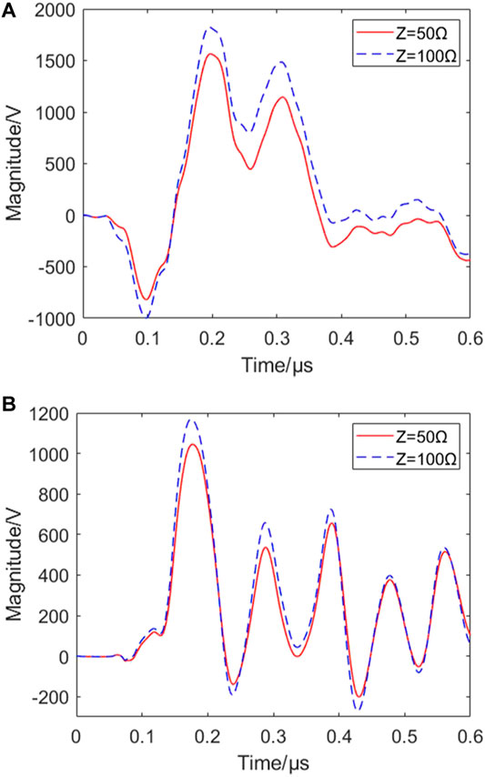
FIGURE 13. Conducted disturbance voltage of secondary cable at different terminal impedance. (A) Capacitive conducted disturbance. (B) Resistive conducted disturbance.
The calculation results show that the amplitude of conducted disturbance voltage increases with the increase of terminal impedance. The reason for the analysis is that when the terminal impedance amplitude increases, the difference between the wave impedance of the secondary cable and the terminal impedance is more significant, resulting in a more intense wave refraction and reflection process. In addition, the increase of terminal impedance has a more significant impact on capacitive conducted disturbance. When the terminal impedance increases from 50 to 100 Ω, the amplitude of capacitive conducted disturbance voltage increases by 0.3 kV, while the amplitude of resistive conducted disturbance voltage increases only by 0.1 kV.
In Zhang et al. (2013), based on the 1000-kV GIS test circuit simulated in this study, UHV VFTO has measured the disturbance voltage of the secondary cable, and compared the disturbance voltage on the secondary cable core under three different grounding modes: grounding at both ends of the secondary cable shield, single-end grounding at the side of the control cabinet, and single-end grounding at the side of the switch station, which are 395, 295, and 4557 V respectively. The following data are obtained during the simulation of the overall disturbance in this study: for the three different grounding methods of the two ends of the secondary cable shielding layer, the single-ended grounding on the control cabinet side, and the single-ended grounding on the switch station side, the overall disturbance voltages are 2.7, 1.5, and 8.0 kV respectively. Comparing the measurement results of the literature with the simulation results of this study, the following two points of analysis can be obtained:
1) Regardless of the measured voltage or the conducted disturbance voltage obtained by simulation in this paper, the disturbance voltage at the end of the secondary cable core is the highest when the shielding layer on the switchyard side is grounded at a single end, and the disturbance voltage is significantly lower than that on the switchyard side under the two methods of grounding at both ends and single-end grounding on the centralized control cabinet side.
2) The simulation results do not correspond to the measured results in the literature. The reasons are as follows: (a) The measured disturbance voltage includes conduction disturbance and radiation disturbance, and the simulation results in this paper only include conduction disturbance. (b) The simulation conditions in this paper are different from the measured conditions in the literature. In this paper, when analyzing the influence of different grounding modes on the conducted disturbance voltage of secondary cable, the cable length is 20 m, while the measured cable length in the literature is 100 m. Theoretically, the disturbance voltage measured at the end of the core wire will decrease with the increase of the cable length. (c) In the calculation, VFTO and TEV as excitation sources are the measured values under the most serious condition of the test circuit, so the simulation results are strictly considered.
Through the above analysis, it can be seen that although this study has some limitations in the verification of the secondary cable disturbance voltage value, the reasons for the difference between the measured value in the existing literature and the simulation value can be analyzed to verify the correctness of the simulation model establishment method in this study.
Conclusion
In this study, the electromagnetic disturbance to secondary cable caused by the disconnector switching operation in GIS is taken as the research object, and the conducted disturbance in the electromagnetic disturbance is mainly studied. The main research results are as follows:
1) The establishment method of the broadband equivalent circuit model based on the vector fitting method is proposed. The error of amplitude-frequency characteristics and phase-frequency characteristics is not more than 5%, which can meet the needs of calculation accuracy.
2) Under the calculation conditions in this study, the amplitude of conducted disturbance voltage is about 2.5 kV when the shield layer of the secondary cable is grounded at both ends. The amplitude of the capacitive component is higher than that of the resistive component, and the main frequency of the resistive component is higher than that of the capacitive component.
3) The research results of influencing factors of conducted disturbance show that with the increase of cable length, the amplitude of disturbance voltage will gradually decrease, and the high-frequency component will significantly decrease. The grounding mode of the cable shield layer has an obvious influence on conducted disturbance, and it has a good shielding effect by way of single-end grounding on the side of the control cabinet or two-end grounding. With the increase of grounding wire length, the potential difference between the grounding point of the secondary cable shield layer and the transient current flowing through the shield layer gradually decreases, and the amplitude of conducted disturbance voltage also decreases.
Data Availability Statement
The raw data supporting the conclusion of this article will be made available by the authors, without undue reservation.
Author Contributions
XC: methodology and conceptualization; ZH: methodology, data analysis, writing original draft, and recording image; YZ: methodology, draft review, and editing; SW: data collection, draft review, and editing; JS: simulation, draft review, and editing; BW: funding acquisition; JL: funding acquisition.
Funding
This research was funded by Open Fund of State Key Laboratory of Power Grid Environment Protection (No. GYW51202001551).
Conflict of Interest
ZH was employed by State Grid Shaoxing Power Supply Company.
The remaining authors declare that the research was conducted in the absence of any commercial or financial relationships that could be construed as a potential conflict of interest.
Publisher’s Note
All claims expressed in this article are solely those of the authors and do not necessarily represent those of their affiliated organizations, or those of the publisher, the editors, and the reviewers. Any product that may be evaluated in this article, or claim that may be made by its manufacturer, is not guaranteed or endorsed by the publisher.
References
Bo, Z. Q., Lin, X. N., Wang, Q. P., Yi, Y. H., and Zhou, F. Q. (2016). Developments of Power System Protection and Control. Prot. Control. Mod. Power Syst. 1 (1). doi:10.1186/s41601-016-0012-2
Cai, Y., Guan, Y., Liu, W., and He, J. (2018). Study of Transient Enclosure Voltage Coupling to Secondary Cables in a Gas-Insulated Substation. IEEE Trans. Power Deliv. 33 (2), 761–768. doi:10.1109/tpwrd.2017.2688406
Chen, W., Li, Z., Sun, G., Dai, M., Liu, W., Li, C., et al. (2011). Experimental Research on the Characteristics of Very Fast Transient Overvoltage in Ultra High Voltage Gas Insulated Switchgear. Proc. Chin. Soc. Electr. Eng. 31 (31), 38–47. (In Chinese). doi:10.13334/j.0258-8013.pcsee.2011.31.009
CIGRE Working Group 33/13.09 (1988). Very Fast Transients Phenomena Associated with Gas Insulated Substations. France: CIGRE.
D'Souza, M., Dhara, R. S., and Bouyer, R. C. (2020). Modularization of High Voltage Gas Insulated Substations. IEEE Trans. Ind. Applicat. 56 (5), 4662–4669. doi:10.1109/tia.2020.3006463
Deschrijver, D., Mrozowski, M., Dhaene, T., and De Zutter, D. (2008). Macromodeling of Multiport Systems Using a Fast Implementation of the Vector Fitting Method. IEEE Microw. Wireless Compon. Lett. 18 (6), 383–385. doi:10.1109/lmwc.2008.922585
Feng, L., Wang, X., Jiang, X., Liu, H., Wang, J., Zhang, X., et al. (2014). Research on the EMC Modeling within the GIS in the EHV Substations. High Voltage Apparatus 50 (4), 97–102. (In Chinese). doi:10.13296/j.1001-1609.hva.2014.04.018
Gustavsen, B., and Semlyen, A. (1998). Application of Vector Fitting to State Equation Representation of Transformers for Simulation of Electromagnetic Transients. IEEE Trans. Power Deliv. 13 (3), 834–842. doi:10.1109/61.686981
Hu, R., Cui, X., Chen, W., Zhang, W., Li, Z., and Dai, M. (2015). Development of the Measuring Device of Transient Enclosure Voltage in Ultra High Voltage Gas Insulated Switchgear. Proc. Chin. Soc. Electr. Eng. 35 (23), 6235–6245. (In Chinese).
Hu, R. (2016). Research on the Characteristics of Electromagnetic Transient Generated During Switching of Disconnector in AC Ultra High Voltage Gas Insulated Switchgear. Beijing: North China Electric Power University Press. (In Chinese). doi:10.13334/j.0258-8013.pcsee.2015.23.032
IEC 61000 (1997). Electromagnetic Compatibility (EMC), Part 5: Installation and Mitigation Guidelines, Section 2: Earthing and Cabling, 1–72. BSI Standards Limited.
IEEE Std 1143™-2012 (2012). “IEEE Guide for the Design and Installation of Cable Systems in Substations,” in IEEE STD 525-2007 (Revision of IEEE Std 525-1992/Incorporates IEEE Std 525-2007/Cor1:2008), 1–138. doi:10.1109/IEEESTD.2008.7752756
Jiao, C., Li, M., and Cui, X. (2016). Broadband Equivalent Circuit Model of Bushing for Gas Insulated Switchgear in Ultra High Voltage Substation. Trans. China Electrotechn. Soc. 31 (20), 64–72. (In Chinese). doi:10.19595/j.cnki.1000-6753.tces.2016.20.006
Ma, G.-M., Li, C.-R., Li, X., Zhou, H.-Y., Chen, W.-J., Wang, H., et al. (2017). Time and Frequency Characteristics of Very Fast Transient Overvoltage in Ultra High Voltage Substation. IEEE Trans. Dielect. Electr. Insul. 24 (4), 2459–2468. doi:10.1109/tdei.2017.005687
Mahmood, F., Okamoto, K., and Takaya, K. (2015). “A Study on Conducted Disturbance below 150 kHz from Commercial Power-Conditioning System,” in IEEE International Telecommunications Energy Conference (INTELEC)), Osaka, Japan, October 18–22, 2015.
Moreira, D. C., Nunes, M. V. A., Moreira, D. D. C., and Costa, D. K. D. (2020). Analysis of VFTO during the Failure of a 550-kV Gas-Insulated Substation. Electric Power Syst. Res. 189, 106825. doi:10.1016/j.epsr.2020.106825
Nan, Y., Di, Y., Zheng, Z., Jiazhan, C., Daojun, C., and Xiaoming, W. (2018). Research on Modelling and Solution of Stochastic SCUC under AC Power Flow Constraints. IET Gener. Transm. Distrib. 12 (15), 3618–3625. doi:10.1049/iet-gtd.2017.1845
Wang, F., and Yang, M. (2016). Fast Electromagnetic Transient Simulation for Over‐voltages of Transmission Line by High Order Radau Method and V ‐transformation. IET Gener. Transm. Distrib. 10 (14), 3639–3645. doi:10.1049/iet-gtd.2016.0476
Wang, H. (2010). Extraction of the Wide-Band Network Parameters and Transient Simulation of the Secondary cable in the Substation. Beijing: North China Electric Power University Press. (In Chinese).
Yang, N., Yang, C., Wu, L., Shen, X., Jia, J., Li, Z., et al. (2021). Intelligent Data-Driven Decision-Making Method for Dynamic Multi-Sequence: An E-Seq2Seq Based SCUC Expert System. IEEE Trans. Ind. Inf., 1. doi:10.1109/TII.2021.3107406
Zhang, B., Hao, Z., and Bo, Z. (2016). New Development in Relay protection for Smart Grid. Prot. Control. Mod. Power Syst. 1 (1). doi:10.1186/s41601-016-0025-x
Zhang, J., He, J., Zhao, J., Zhang, Y., and Zhang, W. (2014). “Characteristics Analysis of Switching Transient Disturbance to Secondary Equipment Port of 1,000 kV Substation,” in International Conference on Power and Energy, Shanghai, China, November, 2014 (CRC Press/Balkema), 443–448.
Keywords: disconnector switching operation, broadband equivalent circuit model, finite integral method, overall electromagnetic disturbance, suppression measures
Citation: Chen X, He Z, Zhang Y, Si J, Wang S, Wan B and Liu J (2022) Research on Conducted Disturbance to Secondary Cable Caused by Disconnector Switching Operation. Front. Energy Res. 9:819021. doi: 10.3389/fenrg.2021.819021
Received: 20 November 2021; Accepted: 01 December 2021;
Published: 07 January 2022.
Edited by:
Xun Shen, Tokyo Institute of Technology, JapanReviewed by:
Wangling He, North China Electric Power University, ChinaPeng Li, China Three Gorges University, China
Copyright © 2022 Chen, He, Zhang, Si, Wang, Wan and Liu. This is an open-access article distributed under the terms of the Creative Commons Attribution License (CC BY). The use, distribution or reproduction in other forums is permitted, provided the original author(s) and the copyright owner(s) are credited and that the original publication in this journal is cited, in accordance with accepted academic practice. No use, distribution or reproduction is permitted which does not comply with these terms.
*Correspondence: Xiaoyue Chen, Y2hlbnhpYW95dWVAd2h1LmVkdS5jbg==