 Robert T. Piper
 Trey B. Daunis1
 Julia W. P. Hsu
- 1Department of Materials Science & Engineering, University of Texas at Dallas, Richardson, TX, United States
- 2NovaCentrix, Austin, TX, United States
High-throughput roll-to-roll (R2R) manufacturing of perovskite solar cells (PSCs) is currently limited by thermal processes that take tens of minutes each, translating to impractically long annealing tools at high web speeds. In addition, PSCs are usually made with metal oxide transport layer materials that require high temperatures for thermal annealing. Here, we demonstrate the fabrication of PSCs using photonic curing, instead of thermal annealing, to convert NiOx directly from sol-gel precursors for hole transport layers and to crystallize methylammonium lead iodide (MAPbI3) active layers on flexible Willow® Glass substrates. Photonic curing uses short, intense pulses of light to process materials at a high speed, hence it is compatible with R2R manufacturing. We achieved power conversion efficiencies (PCEs) of 11.7% in forward-scan and 10.9% in reverse-scan for PSCs made with photonic cured NiOx and MAPbI3 films. Furthermore, both NiOx and MAPbI3 films could be processed with a single photonic curing pulse, with a web speed of 5.7 m/min, and still produce PCEs comparable to thermally annealed control samples. Based on the single-pulse photonic curing condition for each film, we project a web speed of 26 m/min, laying a pathway to high-throughput production of perovskite solar modules.
Introduction
Halide perovskite solar cell (PSC) efficiencies have increased dramatically in the past decade, with power conversion efficiencies (PCE) exceeding 25% for single-junction devices (NREL, 2019). Halide perovskites can be deposited with solution methods and processed at low temperatures, making them a good candidate for roll-to-roll (R2R) printing processes on flexible substrates (Li et al., 2018; Jena et al., 2019). With a 1.5 m wide web moving at a web speed of 30 m/min, R2R processing of PSC could provide up to 4 GW/year for a single R2R assembly line (EMC, 2020). Solution-deposition approaches, including printing (ink-jet, screen, gravure, flexography) and coating (blade, slot-die, spray) methods, have already been developed and can exceed 10 m/min, hence they are compatible with R2R manufacturing (Søndergaard et al., 2013; Abbel et al., 2018). However, metal oxide electron transport layers (ETLs) and hole transport layers (HTLs) for PSCs typically require a high temperature (>100°C) annealing step to fully achieve the desired electronic properties. High temperature annealing can cause substrate damages or mechanical failures, particularly when processing on plastic substrates that have low glass transition temperatures. In addition, plastic substrates typically have a coefficient of thermal expansion mismatch with the transparent conducting oxide layer, which may lead to cracking or delamination in these layers during processing. Recently, significant efforts have been made to reduce annealing temperatures of metal oxide materials to enable fabrication on flexible, plastic substrates (Shin et al., 2019). Reducing the thermal annealing temperature is a step in the right direction, but typical thermal annealing processes require samples to be at elevated temperatures for tens of minutes and are a major bottleneck in achieving a desired R2R speed. For example, an annealing time of 20 min at a web speed of 30 m/min would require a web length of 600 m within a furnace. A furnace this large would demand a huge physical space for the R2R system, emit lots of excess heat, and drive the manufacturing cost up.
One promising alternative to thermal annealing that has received a lot of recent attention is photonic curing, or intense pulsed light annealing (Schroder et al., 2006). In photonic curing, energy from a short (0.03–100 ms) pulse of broadband light (200–1,500 nm) is converted to heat selectively within light-absorbing layers in thin-film samples, resulting in rapid transformations and reactions. While the intensity can be high, the total energy is low because of the short pulse duration. Two major advantages of photonic curing compared to thermal annealing are shorter processing time and compatibility with low heat-tolerant, transparent substrates. Photonic curing has been used to sinter printed metal nanoparticle inks to make conductive traces on flexible substrates (Schroder, 2011; Akhavan et al., 2017). It has also been demonstrated for fabricating ZrO2 (Daunis et al., 2020) and HfO2 (Tetzner et al., 2014) dielectric films from sol-gel precursors on flexible and rigid substrates, respectively. For PSCs, a few research groups have demonstrated that photonic curing can convert perovskite active layers (Lavery et al., 2016; Troughton et al., 2016; Muydinov et al., 2018; Xu et al., 2020). Separately, photonic curing has also been reported for making mesoporous or compact TiO2 (Das et al., 2016; Feleki et al., 2017; Luo et al., 2017) or SnO2 (Zhu et al., 2017) ETLs with thermally annealed perovskite active layers. Most recently, Ghahremani et al. (2020) have applied photonic curing to dry SnO2 nanoparticle ETLs and crystallize triple cation perovskite active layers on the same device, using multiple pulses for each layer. However, no work has been done so far on converting metal oxide semiconductors from sol-gel precursors with photonic curing for use as transport layers in PSCs.
Sol-gel precursor films require high annealing temperatures (∼250°C for NiOx) to form a dense semiconducting metal oxide film (Liu et al., 2018). So far, most reports of low-temperature processing of NiOx HTLs use pre-synthesized NiOx nanocrystal suspensions (Yin et al., 2016; Zhang et al., 2017). Pre-synthesis of nanocrystals requires an additional, time-consuming processing step which increases the manufacturing costs (Wang et al., 2017). Therefore, it is advantageous to develop a one-step process to convert the NiOx HTL from its sol-gel precursor. In this report, we demonstrate the use of photonic curing for converting NiOx HTLs from nickel nitrate sol-gel precursor films on flexible indium tin oxide (ITO) coated Corning Willow® Glass (WG) substrates. Nickel nitrate was chosen as the sol-gel precursor for the NiOx HTL because nickel nitrate sol-gel precursors exhibit a lower decomposition temperature than other commonly used NiOx precursors (Supplementary Figure S1; Liu et al., 2018; Sun et al., 2019). Therefore, less energy is required to convert nickel nitrate precursor to a dense metal oxide film using photonic curing.
For this study, we fabricated inverted planar p-i-n architecture PSCs with the following device structure, listed from bottom to top: WG/ITO/NiOx/methylammonium lead iodide (MAPbI3)/Phenyl-C61-butyric acid methyl ester (PC61BM)/bathocuproine (BCP)/Al. We demonstrate photonic curing for both the NiOx HTL and MAPbI3 active layer on the same device, i.e., a device without any thermal annealing step, and achieve performance comparable to a device with all layers processed by thermal annealing. We also uncover the source of observed performance reduction for PSCs made on WG/ITO substrates compared to on 1 mm Glass/ITO. By eliminating all thermal annealing steps from our process, we reduce the total annealing time from 55 min to 11 s. Furthermore, we show that NiOx HTLs can be converted with just a single photonic curing pulse, further reducing the total annealing time for both layers to 21 ms. Finally, we discuss pathways to reach desired R2R web speeds using commercially available industrial equipment. By applying photonic curing to convert two layers of PSCs from precursors to final products for the first time, this work demonstrates an approach to fabricate flexible PSCs conducive to upscaling to high-throughput manufacturing.
Materials and Methods
Solar Cell Fabrication
Unless otherwise stated, all chemicals are purchased from Sigma-Aldrich and used as purchased. ITO coated 100 µm thick WG (Fraunhofer FEP) or ITO coated 1 mm thick glass (Kintec) were used as substrates. The 1 mm Glass/ITO substrates were rinsed sequentially in soapy water, acetone, IPA, and DI water and dried with N2. The WG/ITO substrates were only blown with N2 without chemical cleaning. Both substrates were UV-ozone treated (Bioforce Nanosciences Procleaner Plus) for 20 min before film deposition. NiOx precursor solution was made, modified from Liu et al. (2018), by dissolving 0.1 M nickel nitrate hexahydrate and 0.1 M acetylacetone in 2-methoxyethanol and stirring overnight at room temperature. The NiOx precursor solution was filtered through a 0.2 µm polytetrafluoroethylene (PTFE) filter before spin coating at 3,000 rpm for 30 s followed by drying on a hot plate at 70°C for 3 min. For thermal annealed (TA) NiOx, the dried precursor films were calcinated on a hot plate at 250°C for 45 min. For photonic cured (PC) NiOx, the samples were processed per Photonic Curing immediately after drying. The NiOx coated samples were then loaded into an N2-purged glovebox to deposit the active layer. MAPbI3 precursor solution was made, following Ahn et al. (2015), by dissolving lead (II) iodide (TCI America), methylammonium iodide (GreatCell Solar), and dimethyl sulfoxide (equal molar ratio) in N,N-dimethylformamide. The MAPbI3 precursor solution was filtered through a 0.2 µm PTFE filter before spin coating at 4,000 rpm for 25 s inside an N2-purged glovebox. After spinning for 10 s, 1 ml of diethyl ether was applied to the sample. For TA MAPbI3, the samples were immediately annealed on a hot plate in the same glovebox at 100°C for 10 min. For PC MAPbI3, the samples were removed from the glovebox immediately after spin coating and processed per Photonic Curing before returning to the glovebox to deposit the ETL. PC61BM (Solenne BV) in chlorobenzene (13 mg/ml) was spin coated at 1,200 rpm for 60 s followed by spin coating bathocuproine (BCP) in ethanol (0.5 mg/ml) at 4,000 rpm for 30 s to create the ETL. No annealing step was required for the ETL. The top contact was deposited by thermally evaporating 100 nm of Al through a shadow mask.
Spectroscopic Ellipsometry
Spectroscopic ellipsometry measurements (M-2000DI, J. A. Woolam) were done at 55°, 65°, and 75° incident angles from 192 to 1,690 nm in wavelength to obtain the index of refraction (n) and extinction coefficient (k) for each material. Uncoated WG, WG/ITO, WG/ITO/NiOx-precursor and 1 mm Glass/ITO were measured with transparent tape adhered to the backside of the samples to eliminate back-side reflections. The NiOx, MAPbI3, PC61BM, and Al films were deposited on single side polished Si wafers, following the same deposition procedures as Solar Cell Fabrication, for the measurement. The data were fitted using Complete Ease software to determine the optical constants and thickness of each film. The fitting for WG was performed using a Cauchy model parameterized into a general oscillator. The ITO coated on WG was fitted using the previously determined WG optical constants to obtain the optical constants of the ITO film. The fitting for ITO on WG starts with a general oscillator function that was first fitted over a limited wavelength range then converted into a B-spline model. The B-spline model was then expanded over the full wavelength range and parameterized into a general oscillator. The fitting for NiOx-precursor on WG/ITO used a B-spline model and the optical constants of the WG/ITO. Fits for NiOx, MAPbI3, PC61BM, and Al were obtained using B-spline models and the optical constants of the Si substrates. A B-spline model was also used for the ITO on 1 mm Glass with the optical constants for the glass taken from Rubin (1985). All fits had a mean square error of less than 9.
Photonic Curing
Photonic curing was done using a NovaCentrix PulseForge® Invent equipped with one 500 V lamp driver, 1.5 kW power supply, and 20 mm (diameter) × 150 mm (length) xenon flash lamp (75 mm × 150 mm illumination area). All photonic curing was performed in ambient conditions (22–24°C, 30–50% RH). The processing stage height was adjusted to be as close to the lamp as the machine allows. The WG/ITO/NiOx samples were suspended between two pairs of magnetic steel slats such that there was an air gap below the sample, between the WG substrate and the processing stage, during photonic curing. MAPbI3 samples were placed directly on the processing stage and held down by two magnetic steel slats for photonic curing.
The radiant energy at each PC processing condition was measured using a calibrated bolometer five separate times to get an average value. The bolometer was also used to determine the surface absorption of the WG/ITO/NiOx-precursor sample by measuring the radiant energy with and without the sample over the bolometer. The difference in the radiant energy measured with and without the sample, minus 8.8% substrate reflection, was used as the surface absorption of the sample for SimPulse® simulations. The 8.8% reflection value was determined by performing the same measurement on an uncoated WG sample and assuming that the WG absorbs no light, which is quite accurate (Supplementary Figure S2). The WG/ITO/NiOx-precursor and uncoated WG samples were pulsed with a lamp voltage of 200 V and a pulse length of 4 ms five separate times and the average radiant energy was used for calculations. The standard deviation in radiant energy for each set of bolometry measurements was less than 1%. This method estimates the surface absorption for WG/ITO/NiOx-precursor is 18%.
Simulations
The percentage of WG/ITO/NiOx-precursor absorption can also be calculated with 1D transfer matrix method (TMM) (Burkhard et al., 2010) using the xenon lamp spectrum (NovaCentrix, 2020) as the source and n and k of WG/ITO/NiOx-precursor obtained from spectroscopic ellipsometry for the sample. We obtained 16% using the TMM method, which is consistent with the bolometry method described in Photonic Curing. The UV-vis spectrum of a dilute NiOx-precursor solution is shown in Supplementary Figure S3.
Simulations of film surface temperature vs. time were generated using NovaCentrix SimPulse® software. The parameters input into the software were the PulseForge® configuration (used to model the lamp output), the measured light absorption by the sample, the material properties (i.e., thermal conductivity, specific heat, and density) from literature, and the measured sample thickness. Note that SimPulse® only models the light absorption and thermal transfer processes and does not take into account any photochemical processes that may occur during photonic curing (Daunis et al., 2020). The WG/ITO/NiOx-precursor sample stack was modeled as 100 µm borosilicate glass and 150 nm ITO. The simulations were done in surface absorption mode using 18% absorption determined from the bolometry measurement as described in Photonic Curing. Using the TMM calculated 16% surface absorption value will only affect the simulated temperature values, but will not change the conclusions drawn from SimPulse® results. Because the NiOx-precursor layer is only ∼30 nm thick, it is much thinner than the thermal length and is not included in the SimPulse® model stack. It is treated as a surface absorbing layer with its contribution measured by bolometry. SimPulse® assumes that the light pulse is absorbed at the surface of the sample and the heat generated there is either conducted down through the sample stack, raising the overall sample temperature, or removed from the sample via convective heat transfer to air from the top and bottom surfaces. The sample is suspended and has air above and below it. SimPulse® models this boundary condition using a convective heat transfer coefficient of 15 W/m2K at the top and bottom sample surfaces. The assumption that the heat is generated at the top surface is reasonable because most of the light is absorbed in the NiOx-precursor and ITO layers, which account for only 0.18% of the entire stack thickness.
Short-circuit current (JSC) calculations were performed by TMM with an AM 1.5G 100 mW/cm2 light source. Two different material stacks were used (Supplementary Figure S4A) to model the different substrates: WG/ITO and 1 mm Glass/ITO. The device layers, consisting of 10 nm NiOx, 450 nm MAPbI3, 50 nm PC61BM, and 100 nm Al, were the same for both substrates. The optical constants and thickness of the sample layers were determined from spectroscopic ellipsometry, except for 1 mm Glass, as described in Spectroscopic Ellipsometry. The TMM calculations assume the MAPbI3 active layer has an internal quantum efficiency of 100%, which was reported in Yang et al. (2015).
Materials and Device Characterization
Current density-voltage (J-V) measurements were performed using an AM 1.5G 100 mW/cm2 AAA solar simulator (Abet) and 2635A Keithley source-meter to conduct forward, −0.2 to 1.2 V, and reverse, 1.2 to −0.2 V, scans under illumination. The illumination area was 0.049 cm2 and the voltage scan rate was 70 mV/s. J-V measurements were performed inside of an N2-filled glovebox after the samples had been stored in it overnight.
UV-vis absorption measurements were obtained using an Ocean Optics 4000 USB spectrometer. Film roughness was measured using an atomic force microscope (AFM, Asylum MFP-3D). Sheet resistance was measured with the four-point van der Pauw method with a Lake Shore 8400 HMS on at least three 1 cm × 1 cm films. Thermogravimetric analysis was conducted using a TA Instruments Q600 on 5–10 mg samples prepared by evaporating precursor solution. The heating rate is 5°C/min under 100 ml/min airflow. X-ray diffraction (XRD) was conducted using a Rigaku Ultima III diffractometer with Cu Kα (1.5418 Å) at a scan speed of 2°/min. Scanning electron microscope (SEM) images were taken with a Zeiss Supra 40 scanning electron microscope at an accelerating voltage of 10 kV. We analyzed MAPbI3 grains in low magnification SEM images (Supplementary Figure S5) using ASTM E112-13 (ASTM International, 2013).
XPS was performed on an Ulvac-PHI VersaProbe2 with a monochromated Al Ka source (1,486.8 eV) at an angle of 45° to the sample surface at 50 W and 15 kV with a 200 µm beam size. Ni 2p3/2 spectra were averaged over 20 scans with an energy step of 0.1 eV at 20 ms per step and a pass energy of 23.5 eV. N 1s spectra were averaged over five scans with an energy step of 0.8 eV at 20 ms per step and a pass energy of 187.85 eV. XPS data were analyzed using commercial software (MultiPak, Ulvac-PHI). The area under the N 1s curve was calculated from 401 to 413 eV with the background taken as a straight line between the two endpoints. The Ni 2p3/2 data for each sample was fitted to seven peaks, with peak 1 at the lowest binding energy and peak seven at the highest binding energy. The position of peak 1 was fitted for each sample (ranging from 853.91 eV for the 2-pulse film to 854.71 eV for the precursor film). The remaining primary peaks (peaks 2, 3, and 4) were set to a fixed binding energy separation from peak 1 of 0.87, 2.1, and 3.62 eV, respectively, based on the best fit for the TA sample. Similarly, the position of the first satellite peak, peak 5, was fitted for each sample while the separation of peaks 6 and 7 from peak 5 was fixed at 2.84 and 5.38 eV, respectively. The full width at half maximum (FWHM) and height for each peak was allowed to vary independently. Due to the non-Gaussian elongated tail observed at the low binding energy edge of the Ni 2p3/2 spectrum, peak 1 was fitted using a mixed Lorentzian-Gaussian function with the Gaussian characteristic allowed to vary from 0 to 100%. All other peaks were restricted to 70–100% Gaussian characteristic.
Results
Photonic Curing NiOx HTL Films and MAPbI3 Active Layers
Scheme 1 depicts the different combinations of TA or PC processes to form NiOx HTLs and MAPbI3 active layers on WG/ITO substrates. Since both layers can undergo TA or PC processes, the resulting PSCs can have four different configurations: TA NiOx + TA MAPbI3 (TA/TA), TA NiOx + PC MAPbI3 (TA/PC), PC NiOx + TA MAPbI3 (PC/TA), and PC NiOx + PC MAPbI3 (PC/PC). The PC61BM, BCP, and Al top layer deposition processes are kept constant. During the NiOx PC process, a xenon flash lamp delivers short, 0.45–10 ms, pulses of light (1–30 pulses) to the sample at repetition rates ranging from 0.1 to 1 Hz and a lamp voltage of 500 or 700 V.
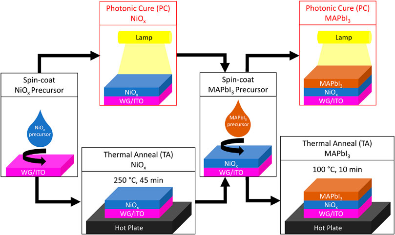
SCHEME 1. Process flow diagram of NiOx and MAPbI3 deposition and annealing steps.
All PC MAPbI3 samples were processed using a single pulse with a lamp voltage of 300 V and a pulse length of 20 ms. This PC processing condition for MAPbI3 was adapted from our previous work on 1 mm glass (Xu et al., 2020), with the lamp voltage reduced for the thinner WG substrates. To compare the PC MAPbI3 conversion on top of TA or PC NiOx HTL, we first conducted XRD to confirm the crystallinity. Figure 1A shows that the underlying NiOx HTL processed by TA or PC has little impact on the crystalline phase of the PC MAPbI3 films. Correspondingly, SEM shows that the PC MAPbI3 films have similar grain size distribution and film morphology (Figures 1B–D).
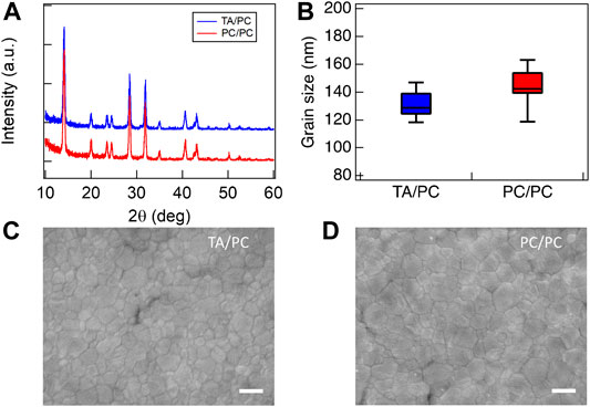
FIGURE 1. (A) XRD patterns of PC MAPbI3 on top of TA and PC NiOx. (B) Statistical analysis based on low magnification SEM images (Supplementary Figure S5). Top-view SEM images of PC MAPbI3 on top of (C) TA NiOx and (D) PC NiOx (scale bar = 200 nm).
Solar Cell Device Performance
Figure 2A shows that PSCs made in the PC/PC configuration exhibit similar champion J-V performance as TA/TA and TA/PC control samples. The PCE values of the champion devices were very similar for all three configurations: 11.5, 12.5, and 11.7%, for TA/TA, TA/PC, and PC/PC, respectively. It is worth noting that the PC/PC devices show less hysteresis than the other two types of devices. Figure 2B shows the average and variation in reverse-scan open-circuit voltage (VOC), JSC, fill factor (FF), and PCE for all three configurations are similar. The NiOx HTLs in the PC/PC devices shown were photonic cured using 500 V lamp voltage, 10 ms pulse length, and 10 pulses at a repetition rate of 0.2 Hz. The inset of Figure 2A shows an image of the flexible WG device. Table 1 contains average reverse-scan PSC device parameters and total NiOx processing time for each photonic curing condition used to process the NiOx HTL.
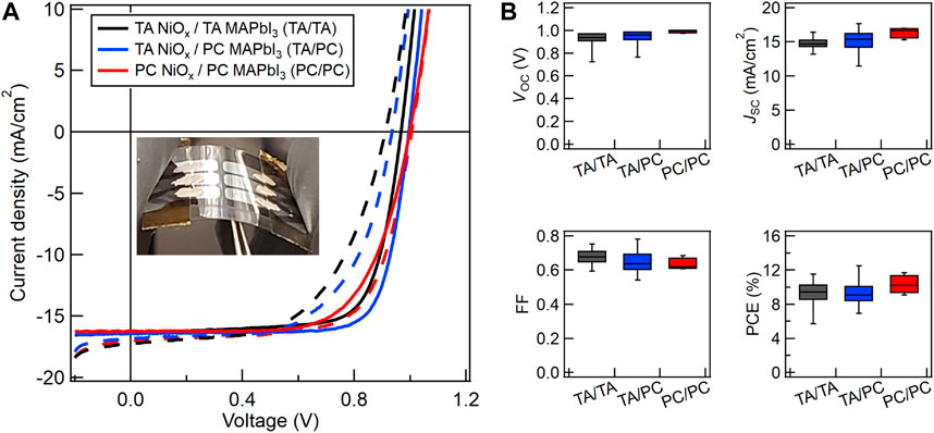
FIGURE 2. (A) Champion reverse (solid) and forward-scan (dashed) device J-V curves for PSCs on WG/ITO fabricated with TA NiOx + TA MAPbI3 (TA/TA, black), TA NiOx + PC MAPbI3 (TA/PC, blue), or PC NiOx + PC MAPbI3 (PC/PC, red). PC NiOx was fabricated at 500 V lamp voltage, 10 ms pulse length, and 10 pulses at 0.2 Hz. The inset is a photograph of a flexible WG PSC device. (B) Box plots of VOC, JSC, FF, and PCE variation measured in reverse-scan for PSCs made with the same conditions listed in (A).
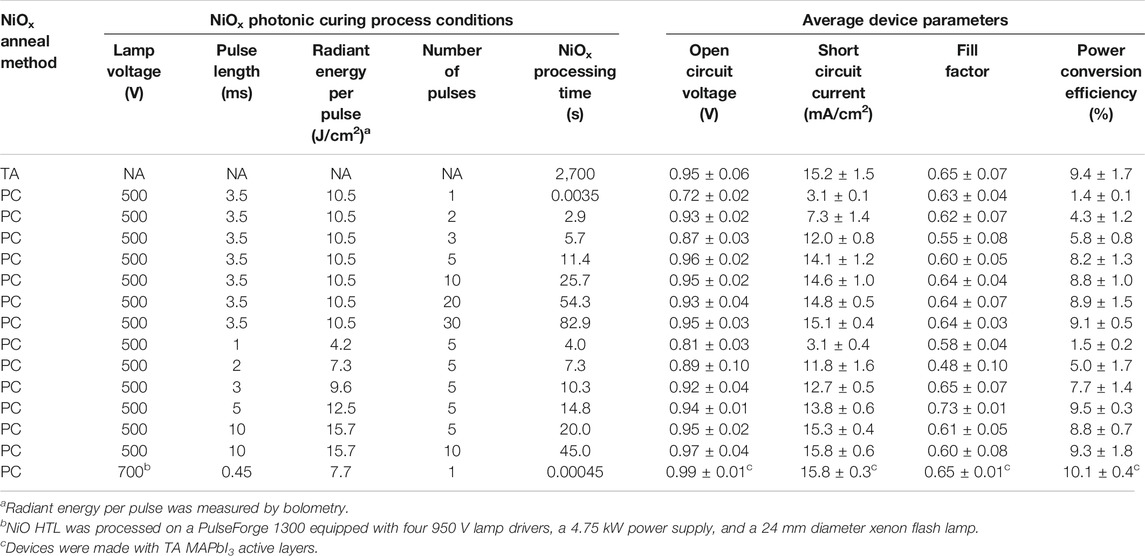
TABLE 1. Average reverse-scan device J-V performance for PSCs made with PC NiOx + PC MAPbI3.
To optimize the process for high-throughput manufacturing, we aim to find the PC processing conditions that can successfully convert NiOx with the shortest time within the PulseForge® Invent’s capability. The maximum lamp voltage of 500 V was selected to maximize the amount of power delivered per pulse. For each pulse condition, the maximum repetition rate allowed by the system was selected to minimize the processing time. The maximum repetition rate depends on the lamp voltage and pulse length, and is limited by how fast the capacitor bank can be recharged by the power supply. At a fixed lamp voltage, longer pulse lengths result in lower repetition rates. More energy is expended within a single pulse for longer pulses because the lamp is on for a longer time; thus, more time is needed to recharge the capacitor banks between pulses. Therefore, with a given tool and a fixed 500 V lamp voltage at the maximum repetition rate, the two independent variables are the pulse length and number of pulses.
At a fixed lamp voltage, the peak sample temperature (Tp) for a single-pulse process increases with pulse length up to a saturation value when the pulse length is longer than a threshold value (t0). For pulses longer than t0, Tp does not increase further with pulse length. Supplementary Figure S6 shows how Tp changes with pulse length at 500 V lamp voltage. For our sample in our tool at the maximum 500 V lamp voltage, t0 equals ∼3 ms. Tp increases with pulse length for pulses <3 ms until it reaches the single-pulse saturation value at ∼ 3 ms. Tp is then equal to the single-pulse saturation value, independent of pulse length, for pulses >3 ms. t0 and the associated single-pulse saturation Tp value depend on the photonic curing tool and parameters used particularly lamp voltage and number of lamp drivers as well as the sample properties and boundary conditions (Xu et al., 2020). Higher lamp voltages will produce higher Tp values for a given pulse length because more power is being delivered to the sample.
We used SimPulse® to calculate the thermal response of the WG/ITO/NiOx-precursor sample under different photonic curing conditions. Figures 3A,B show the simulated thermal response of the sample when processed with a single, 500 V pulse at pulse lengths of 1 ms (<t0) and 5 ms (>t0), respectively. The yellow shaded region indicates the time that the lamp is on. As soon as the lamp turns on, the sample temperature rapidly increases. The lamp intensity is highest when the lamp initially turns on and decreases as the charges in the capacitor bank deplete; therefore, the sample heating rate will decrease throughout the pulse duration. As the sample temperature increases, the cooling rate increases due to convection and conduction of heat away from the sample. When the lamp turns off, the heating rate goes to zero and sample cooling takes over, as evidenced by a steep decrease in temperature past the yellow shaded region. While the cooling rate is initially very fast when the sample surface is at high temperature, the rate decreases as the sample temperature decreases resulting in the temperature returning to ambient over a time period on the order of seconds, which is not shown in these plots. For pulse length shorter than t0, the lamp is turned off during the initial rapid increase in sample temperature, reaching the peak temperature Tp right at the time when the lamp is turned off, as seen in Figure 3A. This Tp value (200°C for 1 ms pulse length) is lower than the single-pulse saturation Tp value (234°C) shown in Supplementary Figure S6 because the sample did not have time to absorb enough radiative energy from the lamp. When pulse length is longer than t0, the cooling rate and heating rate balance each other out at t0 and the single-pulse saturation Tp value is attained. While the lamp is still on past t0, the cooling rate becomes greater than the heating rate, resulting in the temperature declining. This is evident from the slow decrease in temperature between 3 and 5 ms in Figure 3B.
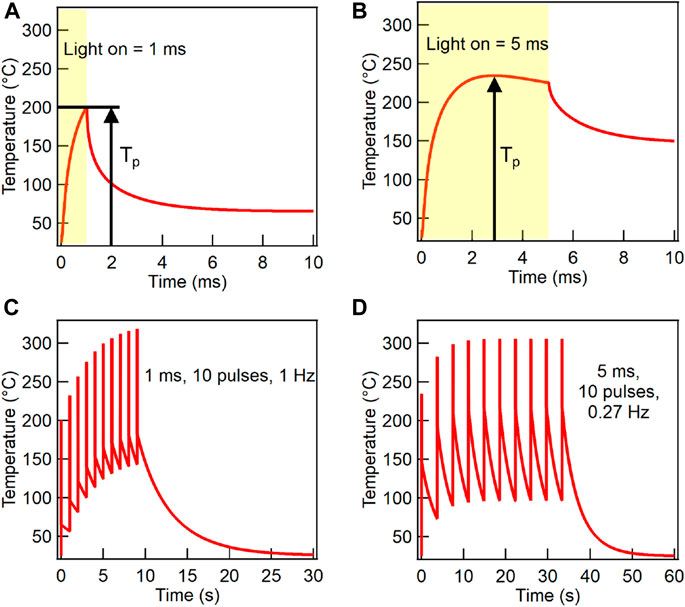
FIGURE 3. SimPulse® generated temperature at the top film surface vs. time of a WG/ITO/NiOx-precursor stack during the photonic curing process for two different pulse lengths and number of pulses at a fixed lamp voltage of 500 V: (A) A single 1 ms pulse. (B) A single 5 ms pulse. (C) Ten 1 ms pulses with a repetition rate of 1 Hz. (D) Ten 5 ms pulses with a repetition rate of 0.27 Hz.
Because our tool is limited to a 500 V capacitor bank, multiple pulses are required to convert the nickel nitrate precursor films to NiOx. Figures 3C,D show the temperature profiles for 10 pulses at 1 ms (1 Hz) and 5 ms (0.27 Hz) pulse lengths, respectively. As previously discussed, the repetition rate is lower for longer pulse length conditions. After the first pulse is finished, and before the sample has time to cool down to ambient temperature, a second pulse is applied. Because the baseline temperature of the sample is now higher than ambient, the second pulse drives Tp to a higher value. As this process is repeated, Tp increases until a multi-pulse saturation value is reached. For a given lamp voltage, multi-pulse saturation Tp is equal to or higher than the single-pulse saturation Tp depending on whether the sample cools down to the ambient temperature in between pulses. The multi-pulse saturation temperature and the number of pulses required to reach it depend on several factors, including pulse length, repetition rate (determined by power supply output), lamp voltage, and number of lamp drivers. For example, Figure 3D shows a multi-pulse saturation Tp of 306°C after four pulses for the 5 ms pulse length condition. In contrast, Tp does not saturate even after 10 pulses for the 1 ms pulse length condition (Figure 3C).
To ensure the maximum possible Tp is achieved, we first chose a pulse length of 3.5 ms and varied the number of pulses to fabricate the NiOx HTL. Figure 4A shows the average (dashed red curve, closed symbols) and champion device (solid red curve, open symbols) reverse-scan PCE results as a function of number of pulses for 3.5 ms pulse length. The PCE values increase with the number of pulses and reach a saturation value of ∼9% above five pulses. Therefore, for fast processing speed while ensuring NiOx is converted, the number of pulses can be reduced to five. Next, we fixed the number of pulses to five and varied the pulse lengths (Figure 4B). A similar trend is observed where PCE values increase significantly at short pulse lengths and saturate above ∼3.5 ms. The black curve and grey shaded area in Figures 4A,B represent the average reverse-scan PCE and one standard deviation, respectively, of devices with TA NiOx HTL, i.e., TA/PC devices, made during the same time frame. Note that all PSCs in Figure 4 are made with PC MAPbI3 active layers. Thus, we demonstrate that NiOx HTLs photonic cured using five 3.5 ms light pulses delivered by 500 V lamp voltage at a repetition rate of 0.35 Hz, translating to 11.4 s of total processing time, produce PSC device performance comparable to NiOx HTLs thermally annealed for 45 min.
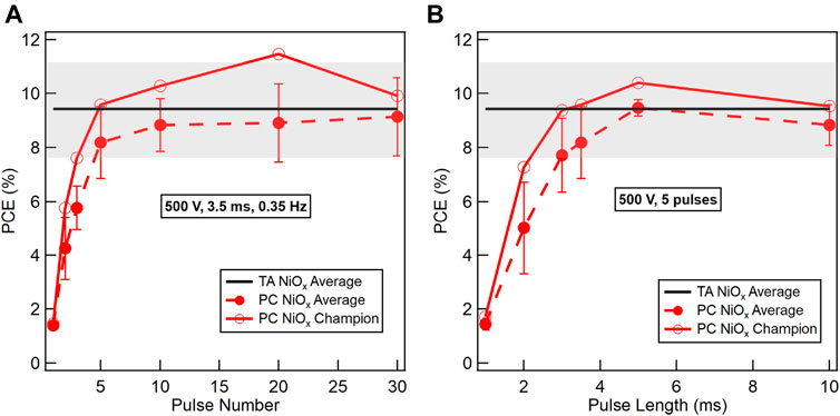
FIGURE 4. Reverse-scan PCE of PSCs on WG/ITO fabricated by different methods. Two parameters are varied in the PC conditions: (A) The number of pulses at fixed pulse conditions of 500 V lamp voltage, 3.5 ms pulse length, and 0.35 Hz repetition rate. (B) The pulse length at fixed pulse conditions of 500 V lamp voltage and five pulses. All PSCs were fabricated with PC MAPbI3 active layers. Average TA NiOx device PCEs are represented by the black line and the standard deviation by the gray area, and the average PC device PCEs are represented by the dashed red curve and closed symbols. The champion PC device PCEs are represented by the solid red curve and open symbols.
To examine the chemical changes in the NiOx film during photonic curing, XPS measurements were performed on NiOx films after photonic curing with 500 V lamp voltage, 3.5 ms pulse length, 0.35 Hz repetition rate, and varying numbers of pulses, as with the devices shown in Figure 4A. The precursor film and thermally annealed film were also measured for comparison. The precursor film has a large N 1s peak at 408 eV due to the nitrate in the precursor solution. The top plot in Figure 5 shows that the area under this peak decreases significantly with an increasing number of photonic curing pulses, and is no longer present after five pulses. The thermally annealed NiO film also shows no N 1s signal. The Ni 2p3/2 measurements and fitted curves are shown in Supplementary Figure S7. The data for each measurement was fitted to seven peaks. The four lower energy peaks are the primary peaks, and the three higher energy peaks are satellite peaks. The energy of the lowest energy peak (peak 1), centered at ∼854.1 eV (not present in the precursor or one pulse films), is attributed to the NiO chemical state (Mansour, 1994b). Peak 2 at ∼855 eV contains contributions from several possible Ni hydroxide species including α and ß-Ni(OH)2, and NiOOH with Ni in the 2+ and 3+ oxidation states (Mansour, 1994a; Mansour and Melendres, 1994; Biesinger et al., 2009). Peak 3 (∼856.5 eV) contains contributions from both the hydroxide species as well as NiO due to multiplet splitting of the primary NiO peak (Mansour, 1994b; Boyd et al., 2020). Peak 4 at highest binding energy (∼858 eV) is attributed to Ni in the 3+ and 4+ oxidation states (Grosvenor et al., 2006). Because only NiO contributes to peak 1 and peak 2 arises from the various hydroxide species with no contributions from NiO, the relative areas of these two peaks, expressed as a percentage of the total area under the four primary peaks, are indicative of chemical transformations from the precursor film to various degree of conversion during photonic curing or after thermal annealing. The results are summarized in the bottom plot in Figure 5. The percent contribution of peak 1 is shown in blue (hashed bars) and that of peak 2 is shown in orange (solid bars). While the sum of the two peaks does not equal 100%, due to contributions from both species in the third and fourth peaks not represented in Figure 5, the percent contributions by two peaks are correlated with the concentration of NiO (blue) and hydroxides (orange) and are independent. Initially, there is no NiO present in the precursor film. After one pulse no NiO has formed (peak 1 remains at 0%), but the contribution of peak 2 to the total primary peak area decreases slightly. During this initial pulse, the nickel nitrate precursor is partially converted to nickel hydroxide, and the total concentration of all hydroxide species increases with their XPS signal shifted from peak 2 to peaks 3 and 4 (Supplementary Figure S7). After two pulses, there is a contribution from peak 1 and a large decrease in the area of peak 2 as the hydroxide species begin to convert to NiO. Additional pulses cause further conversion of hydroxides to NiO, and after 10 pulses the relative contributions from the two peaks are nearly identical to those in the TA sample. The XPS results provide an explanation for the device results in Figure 4A, which show that the PCE for the NiOx HTL processed with five pulses is slightly lower compared to PCE values for NiOx HTLs processed with 10, 20, and 30 pulses. Figure 5 shows that while the N 1s peak is not observed after five pulses, peaks 1 and 2 do not resemble the thermally annealed reference sample until 10 pulses. Therefore, the small difference in PCE values for NiOx HTLs processed with 5 and 10 pulses likely arises from the lower conversion of NiOx at five pulses, as evidenced by the lower peak 1 and higher peak 2 areas.
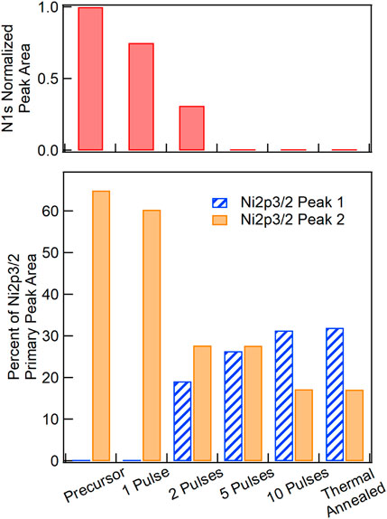
FIGURE 5. XPS N 1s (top) and Ni 2p3/2 (bottom) peak areas for NiOx films photonic cured with varying number of pulses and a NiOx film thermally annealed for reference. N 1s peak areas are normalized to that of the precursor sample. Ni 2p3/2 peak 1 (blue, hashed bars) and peak 2 (orange, solid bars) are expressed as a percentage of the total Ni 2p3/2 primary peak area. Peak 1 is attributed to NiO only and peak 2 is attributed to several Ni hydroxide species. Full Ni 2p3/2 spectra are shown in Supplementary Figure S4.
To explore whether the NiOx HTL can be converted in a single pulse, which will dramatically reduce the total processing time, we employed a PulseForge® 1300 with four 950 V lamp drivers, a 4.75 kW power supply, and a 24 mm diameter lamp. The WG/ITO/NiOx samples were held down by two magnetic steel slats and photonic cured directly on the processing stage. Figures 6A,B show champion device J-V curves and average reverse-scan J-V parameters for PSC devices made in the TA/TA and PC700V/TA configurations. The “700V” sample label denotes that the NiOx HTLs were photonic cured with a single pulse at 700V lamp voltage and 450 µs pulse length. The NiOx samples photonic cured in 450 µs give device performance comparable to the NiOx thermally annealed for 45 min at 250°C. Figure 6C shows a six-order-of-magnitude reduction in processing time when the NiOx HTL was photonic cured with a single pulse.
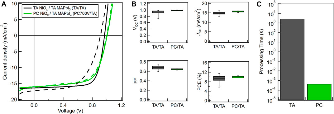
FIGURE 6. (A) Champion forward (dashed) and reverse-scan (solid) device J-V curves for PSCs on WG/ITO fabricated with TA NiOx + TA MAPbI3 (TA/TA, black) or PC NiOx + TA MAPbI3 (PC700V/TA, green) with NiOx photonic cured with a single pulse at 700 V lamp voltage and 450 µs pulse length. (B) Average reverse-scan device VOC, JSC, FF, and PCE for PSCs made with the same conditions listed in (A). (C) Thermal annealing vs. photonic curing processing times (in log scale) for NiOx films made with the same conditions used in (A).
PSC Performance on Flexible vs Rigid Substrates
When transitioning from 1 mm Glass/ITO to flexible WG/ITO substrates, we observed a drop in performance for both champion and average device performance. Upon further examination of the J-V data, there is a ∼13% decrease in JSC when going to the WG/ITO substrate. Figure 7A shows the forward and reverse-scan J-V curves for PSCs made with TA NiOx on the two substrates with the highest JSC value we have measured on each substrate. To understand the discrepancy in JSC, we compared UV-vis transmission spectra, surface roughness, and sheet resistances of both substrates in Figure 7B. The AFM images are shown in Supplementary Figure S8. While the surface roughness and sheet resistance are both higher for WG/ITO compared to 1 mm Glass/ITO, they cannot explain the large JSC discrepancy. Because the NiOx is thermally annealed on a hot plate, a quasi-equilibrium heating process, any performance differences arising from heat transfer or substrate thickness effects during the NiOx annealing are negligible. UV-vis transmission spectra show a significant difference between the two substrates, with WG/ITO having a lower transmission, especially between 300 and 500 nm wavelengths. To determine whether the difference in optical transmission between the substrates is the reason for the decrease in JSC, we determined the ITO optical constants using ellipsometry and then used TMM to calculate the maximum JSC achievable on each substrate (Figure 7C).
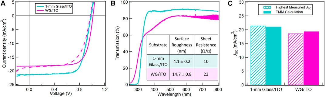
FIGURE 7. (A) Forward (dashed) and reverse-scan (solid) J-V curves for PSCs made with TA NiOx exhibiting the highest measured JSC on either 1 mm Glass/ITO or WG/ITO. (B) UV-vis transmission spectra for 1 mm Glass/ITO and WG/ITO. The inset table shows surface roughness and sheet resistance for both substrates. The sheet resistance for 1 mm Glass/ITO is from vendor data. (C) Highest measured JSC (hashed), i.e., devices in (A), vs. theoretical JSC calculated from TMM (solid). Cyan and magenta represent 1 mm Glass/ITO and WG/ITO, respectively.
Because both WG and 1 mm Glass are optically transparent and can be well fitted with a Cauchy model, the difference in the transmission spectra in Figure 7B must arise from the ITO layers. When fitting the spectroscopic ellipsometry data, the ITO films must be modeled as a graded layer where the optical constants, n and k, vary throughout the thickness of the ITO film. Fits for the ITO film on WG were achieved by modeling the ITO film as five, equally spaced, distinct layers (Supplementary Figure S4A). In contrast, the ITO film on 1 mm Glass only needed two layers in the grading model. The graded models showed good agreement with the measured spectroscopic ellipsometry parameters and optical transmission spectra. The optical constants for the ITO films on each substrate are shown in Supplementary Figures S4B,C. The extinction coefficient for the top-most ITO layer on WG is significantly higher throughout the 300–500 nm wavelength range, which contributes to the lower UV-vis transmission curve for WG/ITO (magenta) in Figure 7B. The n and k for the two layers in 1 mm Glass/ITO are similar, indicating a much more uniform film. The ITO layers on the two substrates are not deposited by the same manufacturer or the same method. The difference in the two materials likely originates from the ITO deposition processes. The WG/ITO was likely deposited using a R2R process where multiple layers of ITO were coated onto the WG sequentially (FraunhoferFEP, 2020).
Finally, we used the optical properties of each substrate to calculate the maximum JSC possible using TMM. The WG/ITO substrate material stack was modeled as 100 µm WG and five 30 nm ITO layers. The 1 mm Glass/ITO substrate material stack was modeled as 1 mm soda lime glass and two 75 nm ITO layers. Both substrate materials stacks were modeled with the same top layers, as described in Simulations. Figure 7C shows an excellent agreement between our highest measured JSC values (hashed bars) and TMM calculations (solid bars) using the models described above and shown in Supplementary Figure S4A. These results show that the optical properties of the ITO film on WG that is commercially available limit the achievable JSC in PSCs. Higher JSC and PCE may be achieved with a different ITO deposition process (Dou et al., 2017), but that is beyond this study.
Discussion
To achieve high-throughput manufacturing of PSCs, alternatives to thermal annealing must be developed. Typically, thermal conversion of metal oxides from sol-gel precursors requires long processing times (minutes to hours), making it incompatible with high-speed R2R manufacturing. R2R processing for our NiOx thermal annealing condition, 250°C for 45 min, and a web speed of 30 m/min would require a least a 1,350 m-long web length within a furnace for processing the NiOx HTL alone. In contrast, photonic curing provides much shorter processing times and lower energy consumption in a smaller physical space than thermal annealing.
We have shown that PSCs made on flexible WG/ITO substrates with photonic cured NiOx HTLs, starting from a sol-gel precursor, and photonic cured MAPbI3 active layers yield an average PCE of ∼10%, with champion devices reaching nearly 12%. These results are in good agreement with thermally annealed NiOx and thermally annealed MAPbI3 control samples on WG/ITO. Thus, we can eliminate all TA steps from our fabrication and achieve a significant reduction in processing time.
For large-area manufacturing, two issues are of particular concern: uniformity and web speed. Xu et al. (2020) have already demonstrated ∼5% variation across 5 inches in the cross-web direction for PC MAPbI3 films. Down-web uniformity using photonic curing for processing is a concern because the light pulses are discrete while the substrate is conveyed at high speed underneath the lamp. To address this issue, stitching must be applied according to Eq. 1:
where f is repetition rate of the light pulses in Hz, s is web speed in ft/min, o is overlap factor, and w is the down-web lamp width in inches (Schroder et al., 2013). For the PulseForge® Invent, the down-web lamp width is 75 mm (3 in). The repetition rate is calculated in SimPulse® considering the specific equipment and pulse conditions used (power supply output, lamp type, number of drivers, lamp voltage, and pulse length). The overlap factor determines the number of pulses received by a point on the sample. An overlap factor of one means that the lamp will only pulse each point on the sample once. Because the light intensity at the edges of the illumination area is lower, it is recommended to use an overlap factor of 1.2 instead of 1. Using an overlap factor of 1.2 will cause subsequent pulses to overlap by 17% and reduce any non-uniformity in the down-web direction.
Using the 700 V single-pulse photonic curing conditions to convert NiOx described above, Eq. 1 yields a web speed of 5.7 m/min using f = 1.5 Hz and o = 1.2. The web speed can be increased by using a larger power supply. For example, increasing the 5 A power supply used in this work to a 45 A power supply, the repetition rate can be increased to process material at a web speed of 13 m/min. Because the web is continuous in R2R processing, the slowest processing step dictates the overall web speed. Performing a similar calculation for the MAPbI3 processing conditions yields a web speed of 18 m/min; hence, the NiOx processing step is the slowest. Faster web speeds can be achieved by machine design and layout considerations. For example, by rotating the 75 mm × 150 mm lamp head by 90°, the processing area can be doubled allowing a web speed of 26 m/min. Placing additional lamps side by side can increase the processing width to meters. Thus, it is feasible to fabricate flexible PSCs using high-throughput photonic curing on both the NiOx HTLs and MAPbI3 active layers, with the potential to scale up to 26 m/min web speeds at arbitrary width. Thus, this work demonstrates the possibility to manufacture perovskite solar modules at a large scale, which will produce lower final product cost due to the economy of scale and reduced energy consumption.
Data Availability Statement
The original contributions presented in the study are included in the article/Supplementary Material, further inquiries can be directed to the corresponding author.
Author Contributions
JH and TD conceived the idea. RP fabricated and measured devices, measured ellipsometry, performed TMM calculations, and wrote the first draft of the manuscript. W.X. participated in device fabrication, determined photonic curing conditions for perovskite on Willow® Glass, and performed four-point van der Pauw, XRD, SEM, TGA, and AFM measurements. TD measured XPS, wrote the corresponding XPS sections of the manuscript, and participated in ellipsometry and photonic curing experiments. TD and KS provided guidance on the design of photonic curing experiments and interpretation of the data. JH supervised the research and contributed to the design of experiments and analysis of results. All authors discussed the data and edited the manuscript.
Funding
RP acknowledges partial support from the National Science Foundation (CBET-1916612). This material is based upon work supported by the U.S. Department of Energy's Office of Energy Efficiency and Renewable Energy (EERE) under the Solar Energy Technologies Office Award Number DE-EE0008544. JH acknowledges support from the Texas Instruments Distinguished Chair in Nanoelectronics.
Disclaimer
This report was prepared as an account of work sponsored by an agency of the United States Government. Neither the United States Government nor any agency thereof, nor any of their employees, makes any warranty, express or implied, or assumes any legal liability or responsibility for the accuracy, completeness, or usefulness of any information, apparatus, product, or process disclosed, or represents that its use would not infringe privately owned rights. Reference herein to any specific commercial product, process, or service by trade name, trademark, manufacturer, or otherwise does not necessarily constitute or imply its endorsement, recommendation, or favoring by the United States Government or any agency thereof. The views and opinions of authors expressed herein do not necessarily state or reflect those of the United States Government or any agency thereof.
Conflict of Interest
Author KS was employed by the company NovaCentrix.
The remaining authors declare that the research was conducted in the absence of any commercial or financial relationships that could be construed as a potential conflict of interest.
Acknowledgments
We thank Energy Materials Corporation for providing the WG/ITO substrates, M. Quevedo for the use of the glovebox and the van de Pauw measurements, R. Wallace for the use of the spectroscopic ellipsometer, and J. Van Derslice for helpful discussion in fitting spectroscopic ellipsometer data for WG/ITO.
Supplementary Material
The Supplementary Material for this article can be found online at: https://www.frontiersin.org/articles/10.3389/fenrg.2021.640960/full#supplementary-material.
References
Abbel, R., Galagan, Y., and Groen, P. (2018). Roll-to-roll fabrication of solution processed electronics. Adv. Eng. Mater. 20, 1701190. doi:10.1002/adem.201701190
Ahn, N., Son, D. Y., Jang, I. H., Kang, S. M., Choi, M., and Park, N. G. (2015). Highly reproducible perovskite solar cells with average efficiency of 18.3% and best efficiency of 19.7% fabricated via lewis base adduct of lead(II) iodide. J. Am. Chem. Soc. 137, 8696–8699. doi:10.1021/jacs.5b04930
Akhavan, V., Schroder, K., and Farnsworth, S. (2017). “Photonic curing enabling high-speed sintering of metal inkjet inks on temperature-sensitive substrates,” in Handbook of industrial inkjet printing: a full system Approach, Editor W. Zapka, (Weinheim, Germany: Wiley-VCH Verlag GmbH & Co. KGaA), 557–566. doi:10.1002/9783527687169.ch32
ASTM International. (2013). ASTM e112-13: standard test methods for determining average grain size. West Conshohocken, PA: American Society for Testing and Materials.
Biesinger, M. C., Payne, B. P., Lau, L. W. M., Gerson, A., and Smart, R. S. C. (2009). X-ray photoelectron spectroscopic chemical state Quantification of mixed nickel metal, oxide and hydroxide systems. Surf. Interf. Anal. 41, 324–332. doi:10.1002/sia.3026
Boyd, C. C., Shallcross, R. C., Moot, T., Kerner, R., Bertoluzzi, L., Onno, A., et al. (2020). Overcoming redox reactions at perovskite-nickel oxide interfaces to boost voltages in perovskite solar cells. Joule 4, 1759–1775. doi:10.1016/j.joule.2020.06.004
Burkhard, G. F., Hoke, E. T., and McGehee, M. D. (2010). Accounting for interference, scattering, and electrode absorption to make accurate internal quantum efficiency measurements in organic and other thin solar cells. Adv. Mater. Weinheim 22, 3293–3297. doi:10.1002/adma.201000883
Das, S., Gu, G., Joshi, P. C., Yang, B., Aytug, T., Rouleau, C. M., et al. (2016). Low thermal budget, photonic-cured compact TiO2 layers for high-efficiency perovskite solar cells. J. Mater. Chem. A. 4, 9685–9690. doi:10.1039/c6ta02105k
Daunis, T. B., Schroder, K. A., and Hsu, J. W. P. (2020). Photonic curing of solution-deposited ZrO2 dielectric on PEN: a path towards high-throughput processing of oxide electronics. Npj Flex. Electron. 4, 7. doi:10.1038/s41528-020-0070-4
Dou, B., Miller, E. M., Christians, J. A., Sanehira, E. M., Klein, T. R., Barnes, F. S., et al. (2017). High-performance flexible perovskite solar cells on ultrathin glass: implications of the TCO. J. Phys. Chem. Lett. 8, 4960–4966. doi:10.1021/acs.jpclett.7b02128
EMC (2020). High speed inline roll-to-roll module production – EMC. Available at: https://enmatcorp.com/high-speed-inline-roll-to-roll-module-production/ (Accessed November 15, 2020).
Feleki, B., Bex, G., Andriessen, R., Galagan, Y., and Di Giacomo, F. (2017). Rapid and low temperature processing of mesoporous TiO2 for perovskite solar cells on flexible and rigid substrates. Mater. Today Commun. 13, 232–240. doi:10.1016/j.mtcomm.2017.09.007
FraunhoferFEP, (2020). Flexible glass - fraunhofer FEP. Available at: https://www.fep.fraunhofer.de/en/highlights/flexibles-glas.html (Accessed November 18, 2020).
Ghahremani, A. H., Martin, B., Gupta, A., Bahadur, J., Ankireddy, K., and Druffel, T. (2020). Rapid fabrication of perovskite solar cells through intense pulse light annealing of SnO2 and triple cation perovskite thin films. Mater. & Des. 185, 108237. doi:10.1016/j.matdes.2019.108237
Grosvenor, A. P., Biesinger, M. C., Smart, R. S. C., and McIntyre, N. S. (2006). New interpretations of XPS spectra of nickel metal and oxides. Surf. Sci. 600, 1771–1779. doi:10.1016/j.susc.2006.01.041
Jena, A. K., Kulkarni, A., and Miyasaka, T. (2019). Halide perovskite photovoltaics: background, status, and future prospects. Chem. Rev. 119, 3036–3103. doi:10.1021/acs.chemrev.8b00539
Lavery, B. W., Kumari, S., Konermann, H., Draper, G. L., Spurgeon, J., and Druffel, T. (2016). Intense pulsed light sintering of CH3NH3PbI3 solar cells. ACS Appl. Mater. Inter. 8, 8419–8426. doi:10.1021/acsami.5b10166
Li, Z., Klein, T. R., Kim, D. H., Yang, M., Berry, J. J., Van Hest, M. F. A. M., et al. (2018). Scalable fabrication of perovskite solar cells. Nat. Rev. Mater. 3, 1–20. doi:10.1038/natrevmats.2018.17
Liu, Z., Chang, J., Lin, Z., Zhou, L., Yang, Z., Chen, D., et al. (2018). High-performance planar perovskite solar cells using low temperature, solution–combustion-based nickel oxide hole transporting layer with efficiency exceeding 20%. Adv. Energ. Mater. 8, 1–9. doi:10.1002/aenm.201703432
Luo, S., Zhang, S., Bourgeois, B. B., Riggs, B. C., Schroder, K. A., Zhang, Y., et al. (2017). Instantaneous photoinitiated synthesis and rapid pulsed photothermal treatment of three-dimensional nanostructured TiO2 thin films through pulsed light irradiation. J. Mater. Res. 32, 1701–1709. doi:10.1557/jmr.2017.139
Mansour, A. N. (1994b). Characterization of NiO by XPS. Surf. Sci. Spectra 3, 231–238. doi:10.1116/1.1247751
Mansour, A. N. (1994a). Characterization of β‐Ni(OH)2 by XPS . Surf. Sci. Spectra 3, 239–246. doi:10.1116/1.1247752
Mansour, A. N., and Melendres, C. A. (1994). Characterization of α‐Ni(OH)2 by XPS . Surf. Sci. Spectra 3, 255–262. doi:10.1116/1.1247754
Muydinov, R., Seeger, S., Vinoth Kumar, S. H. B., Klimm, C., Kraehnert, R., Wagner, M. R., et al. (2018). Crystallisation behaviour of CH3NH3PbI3 films: the benefits of sub-second flash lamp annealing. Thin Solid Films 653, 204–214. doi:10.1016/j.tsf.2018.03.050
NovaCentrix, (2020). Photonic curing FAQ | NovaCentrix. Available at: https://www.novacentrix.com/FAQ (Accessed November 18, 2020).
NREL (2019). Best research-cell efficiency chart. Available at: https://www.nrel.gov/pv/cell-efficiency.html (Accessed May 27, 2020).
Rubin, M.. (1985). Optical properties of soda lime silica glasses. Solar Energ. Mater. 12, 275–288. doi:10.1016/0165-1633(85)90052-8
Søndergaard, R. R., Hösel, M., and Krebs, F. C. (2013). Roll-to-roll fabrication of large area functional organic materials. J. Polym. Sci. B Polym. Phys. 51, 16–34. doi:10.1002/polb.23192
Schroder, K. A., Martin, K. M., Jackson, D. K., and McCool, S. C. (2013). US86746B12. Method and apparatus for curing thin films on low-temperature substrates at high speeds.
Schroder, K. A., McCool, S. C., and Furlan, W. F. (2006). Broadcast photonic curing of metallic nanopartiele films. 2006 NSTI nanotechnol. Conf. Trade show - NSTI nanotech 2006 tech. Proc. 3. Available at: www.nsti.org (Accessed November 18, 2020).
Schroder, K. A. (2011). Mechanisms of photonic curingTM: processing high temperature films on low temperature substrates. Tech. Proc. 2011 NSTI Nanotechnol. Conf. Expo. NSTI-Nanotech 2, 220–223.
Shin, S. S., Lee, S. J., and Seok, S. I. (2019). Metal oxide charge transport layers for efficient and stable perovskite solar cells. Adv. Funct. Mater. 29, 1900455–1900530. doi:10.1002/adfm.201900455
Sun, Y., Chen, W., Wu, Y., He, Z., Zhang, S., and Chen, S. (2019). A low-temperature-annealed and UV-ozone-enhanced combustion derived nickel oxide hole injection layer for flexible quantum dot light-emitting diodes. Nanoscale 11, 1021–1028. doi:10.1039/c8nr08976k
Tetzner, K., Schroder, K. A., and Bock, K. (2014). Photonic curing of sol-gel derived HfO2 dielectrics for organic field-effect transistors. Ceramics Int. 40, 15753–15761. doi:10.1016/j.ceramint.2014.07.099
Troughton, J., Carnie, M. J., Davies, M. L., Charbonneau, C., Jewell, E. H., Worsley, D. A., et al. (2016). Photonic flash-annealing of lead halide perovskite solar cells in 1 ms. J. Mater. Chem. A. 4, 3471–3476. doi:10.1039/c5ta09431c
Wang, K., Shi, Y., Gao, L., Chi, R., Shi, K., Guo, B., et al. (2017). W(Nb)O x -based efficient flexible perovskite solar cells: from material optimization to working principle. Nano Energy 31, 424–431. doi:10.1016/j.nanoen.2016.11.054
Xu, W., Daunis, T. B., Piper, R. T., and Hsu, J. W. P. (2020). Effects of photonic curing processing conditions on MAPbI3 film properties and solar cell performance. ACS Appl. Energ. Mater. 3, 8636–8645. doi:10.1021/acsaem.0c01243
Yang, B., Dyck, O., Poplawsky, J., Keum, J., Puretzky, A., Das, S., et al. (2015). Perovskite solar cells with near 100% internal quantum efficiency based on large single crystalline grains and vertical bulk heterojunctions. J. Am. Chem. Soc. 137, 9210–9213. doi:10.1021/jacs.5b03144
Yin, X., Chen, P., Que, M., Xing, Y., Que, W., Niu, C., et al. (2016). Highly efficient flexible perovskite solar cells using solution-derived NiOx hole contacts. ACS Nano 10, 3630–3636. doi:10.1021/acsnano.5b08135
Zhang, H., Cheng, J., Li, D., Lin, F., Mao, J., Liang, C., et al. (2017). Toward all room-temperature, solution-processed, high-performance planar perovskite solar cells: a new scheme of pyridine-promoted perovskite formation. Adv. Mater. Weinheim 29, 1604695. doi:10.1002/adma.201604695
Keywords: intense pulsed light, perovskite solar cell (PSC), nickel oxide, roll- to-roll (R2R) manufacturing, high throughout, photonic curing, hole transport layer (HTL)
Citation: Piper RT, Daunis TB, Xu W, Schroder KA and Hsu JWP (2021) Photonic Curing of Nickel Oxide Transport Layer and Perovskite Active Layer for Flexible Perovskite Solar Cells: A Path Towards High-Throughput Manufacturing. Front. Energy Res. 9:640960. doi: 10.3389/fenrg.2021.640960
Received: 12 December 2020; Accepted: 12 February 2021;
Published: 26 March 2021.
Edited by:
William J. Scheideler, Dartmouth College, United StatesReviewed by:
Yulia Galagan, National Taiwan University, TaiwanNick Rolston, Stanford University, United States
Copyright © 2021 Piper, Daunis, Xu, Schroder and Hsu. This is an open-access article distributed under the terms of the Creative Commons Attribution License (CC BY). The use, distribution or reproduction in other forums is permitted, provided the original author(s) and the copyright owner(s) are credited and that the original publication in this journal is cited, in accordance with accepted academic practice. No use, distribution or reproduction is permitted which does not comply with these terms.
*Correspondence: Julia W. P. Hsu, andoc3VAdXRkYWxsYXMuZWR1