 Vinod Kumar Kanike
 Saravanakumar Raju
- School of Electrical Engineering, Vellore Institute of Technology, Vellore, India
Pulse width modulation (PWM) methods are used to control the switching sequence operations of conventional multilevel inverters (MLIs) and reduced switch multilevel inverters (RSMLIs). Many researchers proposed various RSMLIs with their switching sequence operation and PWM control techniques. However, the switching operations of RSMLIs are not similar to conventional MLIs, which are a major problem of switch control. Logical equations are proposed for the operation of RSMLIs with the multi-carrier PWM methods like alternative phase opposition disposition (APOD), phase opposition disposition (POD), and phase disposition (PD). To operate the individual switch in symmetrical and asymmetrical RSMLI, logical operators are used to produce required pulse sequence from the sequence of PWM method and their analysis is not present in previous works. The proposed methodology can be applied to PV systems for efficient operation. The proposed methodology and binary representation of PWM method are analyzed on various RSMLIs for seven-level output voltage to operate each individual switch. Control of individual switching sequence and the operation of RSMLIs are simulated using MATLAB/Simulink. THD comparison is presented for RSMLI, DCL MLI, and SCSD MLI with various PWM methods.
Introduction
Reducing the switch count for the design of multilevel inverters (MLIs) has an area of research in MLIs and focused to the study on reduced switch multilevel inverters (RSMLIs) (Vemuganti et al., 2018). Single DC voltage source is used to neutral point clamped MLI, active neutral point clamped MLI, flying capacitor MLI, and modular cascaded MLI. Multiple DC voltage sources are used for cascaded H bridge MLI, diode clamped MLI, and hybrid MLIs. Based on the multiple DC sources voltage ratio, MLIs are classified as symmetrical and asymmetrical (Ali and Kannan, 2015; Prabaharan and Palanisamy, 2017). RSMLIs are also designed by symmetric and asymmetric voltage sources with and without H bridge circuits. Mode of operation for RSMLI is the complex task and is presented as switching sequence table (Kumar and Kumar, 2019a). RSMLIs are proposed to achieve cost minimization, optimal voltage stress, reduced power losses, switching frequency operations, and less harmonic distortions. Operation of these conventional MLIs is performed with the support of gating signals (pulses) to the power switches of the respective inverter design (Chen et al., 2019).
Various modulation methods are used to operate the switches of symmetrical and asymmetrical RSMLIs. Among these, sinusoidal pulse width modulation (PWM), space vector PWM methods, and selective harmonic elimination PWM are most suitable to achieve good efficiency, less switching losses, and less harmonic distortion values (Sudhakar Babu et al., 2015; Kumar and Kumar, 2018). Generation of gating signals is achieved by various pulse modulation techniques with fundamental switching frequency and high switching frequency. There are one or two gating signals per cycle for the switching operation with low switching frequency (50–100 Hz), whereas high switching frequency (2–20 kHz) has multiple gating signals per cycle (Dong et al., 2016; Orfi Yegane and Sarvi, 2018). Multiple high switching frequency is suitable for the operation of RSMLIs with SPWM technique; this will result in the multi-carrier SPWM technique. With respect to the parameter variation of modulation signal, unipolar PWM, level-shifted PWM, and phase-shifted PWM schemes are implemented in the SPWM technique. Similarly, alternative phase opposition disposition (APOD), phase opposition disposition (POD), and phase disposition (PD) are presented with the parameter variation of carrier signal (Carrara et al., 1992; Holtz, 1992; Colak et al., 2011; Vemuganti et al., 2018).
Sequences of switching operation of various RSMLIs are presented in many research works with one of the modulation methods. However, obtaining the required pulse sequence for individual switch in RSMLI is a critical part of the presented works. Obtained pulse sequence from the traditional modulation method is not exactly matching with the required pulse sequence of RSMLI switching operation. Analyzing the proper logical operator for the generation of required pulse sequence is the complex task for the RSMLI operation. Using the logical operations, the working module of various RSMLIs are not properly explained by the researchers in their research works (Krishna and Vadhera, 2013; Umashankar et al., 2013; Gnana Prakash et al., 2014; Uthirasamy et al., 2015). By observing the limitations of the abovementioned works, in this article, the authors proposed the switching operation of RSMLI with the required generation of pulse sequence with unique methodology. In addition, detailed analysis and comparative analysis are also presented to show the superiority of the proposed technique. For better understanding pulse sequence generated by the proposed methodology, other PWM techniques are presented in tabular form.
Wide research studies on various renewable energy sources like photovoltaic and wind energy generation system are presented with various improved parameters. Power electronic converters are used for the integration of various renewable energy sources called hybrid structures. Control aspects of the various power converters are performed to obtain the required system parameters like improved efficiency for PV system and demand side with economical conditions (Dorahaki, 2015; Narendiran and Sahoo, 2017; Dorahaki et al., 2019). Efficiency and economical conditions motivate the authors to propose the control of reduced switch count MLI with simulation analysis. Various controlled methodologies are used for the control of RSMLIs, which are complex. A simple methodology is proposed in the present work with basic logic operators for the pulse sequence operation. A comparative study of various reduced switch count MLIs is presented with switch count (S), diodes (D), capacitors (C), output voltage level, PWM techniques, and methodology applied for the switching operation and is given in Table 1.
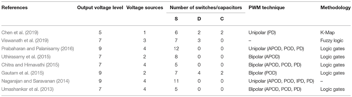
Table 1. Comparison of various reduced switch MLIs.
The organization of the article is as follows: Various RSMLIs of seven-level output voltage is presented in section Reduced Switch Multilevel Inverter (Seven Level). Selection of multi-carriers and various carrier based modulation techniques are given in section Carrier-Based Modulation Technique. Implementation of proposed methodology is discussed in section Implementation of Proposed Methodology. THD values with respect to various modulation index values and results of RSMLIs are presented in section Results and THD Comparison. The proposed methodology for the switching sequence operation of RSMLIs concludes in the final section.
Reduced Switch Multilevel Inverter (Seven Level)
Multistep output voltage of the traditional inverter is obtained with the proper arrangement of power semiconductor switches. Power semiconductor switches in the design of the traditional MLIs are directly operated and controlled with the pulse sequence obtained from multi-carrier PWM methods. These MLIs do not require any intermediate circuit to convert the obtained sequence of pulse to the required pulse sequence. In traditional MLIs, usage of power semiconductor switches, number of DC sources, and linear and non-linear elements are given in Table 2 (Kumar and Kumar, 2019a,b), where L is the level of MLI. Because of the greater number of electrical and electronic components, various parameters like power losses, total harmonic distortion (THD), efficiency, etc., are affecting the traditional MLI designs. To overcome these drawbacks from traditional MLIs, RSMLIs are introduced by many researchers. For the proposed analysis work on PWM, some of the recent RSMLIs are considered from the research work and compared with the performance parameters of the different systems. Intermediate switching circuitry is required for the operation of considered RSMLIs.
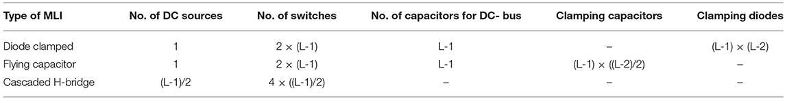
Table 2. Required number of components for traditional MLIs.
Umashankar et al. (2013) proposed a seven-level symmetric RSMLI design with five controllable semiconductor switches and 4 DC voltage sources (VDC). This RSMLI is presented without H bridge and analyzed for the less THD values with resistive load. Chitra and Himavathi (2015) considered the proposed symmetric RSMLI by Umashankar et al. (2013) for the application of induction motor drive. Structure of the seven-level symmetric RSMLI is shown in Figure 1A and the switching sequence for the operation is given in Table A1.
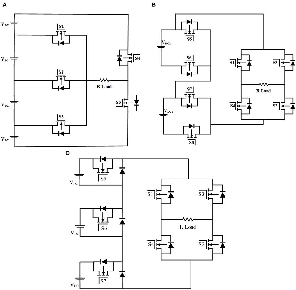
Figure 1. Various seven-level MLIs. (A) Reduced switch MLI. (B) DC link MLI. (C) SCSD MLI.
Uthirasamy et al. (2015) proposed a DC link Cascaded (DCLMLI) seven-level asymmetric RSMLI with H bridge design. Eight controllable switches and 2 DC voltage sources (VDC1, VDC2) are used for the structure of the proposed module. THD result analysis with application to uninterrupted power supply system is done in their research work. Structure of asymmetric RSMLI and the switching sequence are shown in Figure 1B and Table A2.
Viswanath et al. (2019) proposed a symmetric cascaded switched diode (SCSD) seven-level RSMLI with H bridge design. Seven controllable and three uncontrolled switches with three DC voltage sources (VDC) are used for the design of proposed module. Combination of DC voltage source, controllable switch, and uncontrolled switch gives an elementary unit for the operation of the proposed RSMLI. Structural design and switching sequence table are shown in Figure 1C and Table A3. Switching sequence control of the proposed RSMLI is done with a fuzzy controller. THD analysis is presented in the results discussion for various levels.
In these proposed symmetric and asymmetric RSMLI, logical operators are used for individual switch for operating the switch with required switching sequence. Proper pulse conversion analysis is not presented based on carrier modulation techniques in their proposed research. Proper modulation techniques with analysis of logical operators are proposed in the present work.
Carrier-Based Modulation Technique
Various modulation techniques are reviewed for RSMLIs and conclusions with “per-carrier cycle” carrier-based PWM method (Hamman and van der Merwe, 1988; Carrara et al., 1992). Implementation of the carrier-based PWM technique exists in two methods. The direct digital technique has a pre-calculated inverter state, time length of each carrier, and modulation cycle employing space vector theory (Hava et al., 1999; Gopalakrishnan and Narayanan, 2014). The indirect technique works with carrier triangle intersection technique. Reference modulation wave with a low frequency is compared with high-frequency triangular carrier wave and the intersection results in the pulse switching sequence (Dong et al., 2016; Kumar and Kumar, 2018).
In the operation of MLIs, carrier triangular intersection technique is easy to implement with modulation wave comparison strategy. Bipolar sinusoidal wave, unipolar sinusoidal wave, and saw tooth wave are preferable for the modulation wave (Vemuganti et al., 2018). Single triangular carrier wave is suitable for two-level and three-level traditional MLIs. In case of five levels and more than five levels, multi-carrier triangular waves are used for the generation of levels (McGrath and Holmes, 2002). For the analysis of switching sequence in the considered RSMLIs, bipolar sinusoidal (SPWM) wave and unipolar sinusoidal (USPWM) is used as modulation signal. Based on position of multi-carrier waves, phase shift (PS) and level shift (LS) PWM techniques are proposed. Multi-carrier technique is used with three disposition carrier wave implemented as follows (Nagarajan and Saravanan, 2014; Prasad et al., 2017; Chen et al., 2019).
Alternative Phase Opposition Disposition
The arrangement of all triangular carrier waves alternatively in opposition with displacement of 180° to phase is called alternative phase opposition disposition (APOD). All carrier waves are compared with the low-frequency modulation bipolar sinusoidal wave or unipolar sinusoidal wave with preferred amplitude and frequency measured based on the level of MLI. Representation of APOD PWM technique is presented in Figures B1, B2.
Phase Opposition Disposition
Selection of all in-phase carrier waves considered for above zero reference value and all in-phase carrier waves but opposite with displacement of 180° to below zero reference value is called phase opposition disposition (POD). Only bipolar sinusoidal modulation wave is possible in the POD PWM technique. The USPWM method is not possible for the POD PWM technique due to no below zero reference value in unipolar modulation wave. Representation of POD PWM technique is presented in Figure B3.
Phase Disposition
All the triangular carrier waves on above and below zero reference value are in-phase. This modulation technique is called phase disposition (PD). Bipolar and unipolar sinusoidal modulation wave is suitable for the operation of PD PWM technique. Figures B4, B5 show representation of PD PWM technique.
Selection of number of multi-carrier waves for the operation of RSMLI in intersection technique is proposed with proper methodology and shown in Figure 2. Selection of number of carrier signals (C), amplitude of each carrier wave, amplitude of modulation wave (Am) are to be defined based on the level of output voltage. With the proper analysis of the proposed algorithm, generation of gating signals are obtained with the comparison of amplitudes of modulation wave and carrier wave given in Equations (1) and (2).
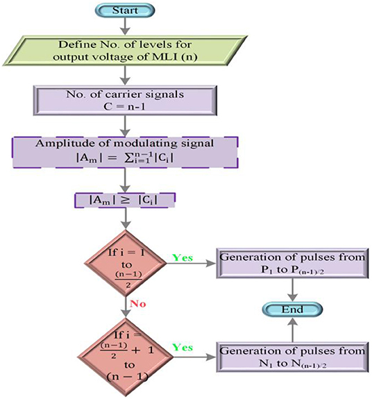
Figure 2. Flowchart for calculation of number of carrier waves and generation of pulses.
In most of the bipolar PWM methods, n−1 carrier signals are used for the “n” level output voltage of RSMLI. (n−1)/2 carrier waves are used for the unipolar PWM methods (Huang et al., 2018). The switching sequence operation of seven-level symmetric RSMLI and asymmetric DCL MLI is performed by bipolar multi-carrier PWM method. SCSD MLI switching sequence operation is done with the unipolar multi-carrier PWM method. Calculation for number of divisions per cycle and time interval of each division is given in Equations (5) and (6). For seven-level output voltage of MLI, total time of one cycle is to be distributed for one cycle as shown in Figure 3.
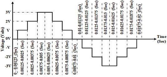
Figure 3. Time distribution of one cycle for seven-level MLI.
To present the clear analysis of switching sequence operation for individual MLI, a binary representation switching sequence is presented in this research work. Binary representation of bipolar SPWM and unipolar SPWM methods is shown in Tables B1, B2.
Implementation of Proposed Methodology
Switching sequences of individual switch in various RSMLI with the binary representation sequence of PWM method are compared to generate the required pulse sequence. Representation of switching sequence is in the form of “0's” and “1's”, and it is easy to analyze the logical equations for the intermediate circuit. If a generated pulse sequence exactly matches any of the individual switching sequence of RSMLI, then the matched sequence is directly used for the operation of proper switch. If pulse sequence does not match any switching sequence, then an intermediate circuit is to be designed with the use of logic gates. Depending on the “ON” and “OFF” condition of a switch in one cycle, the use of logic gates is decided. If a switch is ON and OFF for more times per cycle, then a greater number of logic gates are used for the intermediate circuit. With the observation of irregular ON and OFF condition of a switch, some logical equations are analyzed and presented for individual switch, which do not have direct control from generated pulse sequence of the PWM method. A Karnaugh map is used for the analysis of logical equations (Vemuganti et al., 2018; Chen et al., 2019) for individual switch for five-level RSMLI. Application of K map is complex for the system with more than four variables. For seven-level RSMLI, a minimum of six pulse sequence variables are available.
To compare the sequence of each switch, the generated pulse sequence unique algorithm is proposed in this research work. All the considered RSMLI are of seven levels; six pulse sequences are obtained from the comparison and intersection methods of PWM. Initially, pulse sequences are defined in the comparison operation of the proposed methodology. Pulse sequences obtained from the carrier waves in PWM methods that are above the zero reference wave are considered as binary sequence of positive half cycle. Representation of the positive half cycle pulse sequence variables are P1, P2, and P3. Pulse sequences from carrier waves that are below the zero reference wave are considered as negative half cycle binary sequence. N1, N2, and N3 are the negative half cycle pulse sequence variables. Each switch sequence is divided into two halves, positive half switch sequence (SP) and the negative half switch sequence (SN). Each switch positive half sequence (Sp) is individually compared with single-variable pulse sequence of positive half pulse sequences (P1, P2, and P3). Evaluating analysis of each variable along with its logical NOT operator variables is clearly presented in the flowchart representation as shown in Figure 4A. Similar to comparison of positive half switching sequence and pulse sequence, negative half cycle switching sequence (SN) is compared individually with the single variable of negative half pulse sequences (N1, N2, and N3) and logical NOT operator variables. Zero reference wave variable is represented as PN0. Flowchart representation of the proposed negative half cycle comparison is shown in Figure 4B. If the switching sequence does not match any of individual pulse sequences, then the logical combination of two variables is considered.
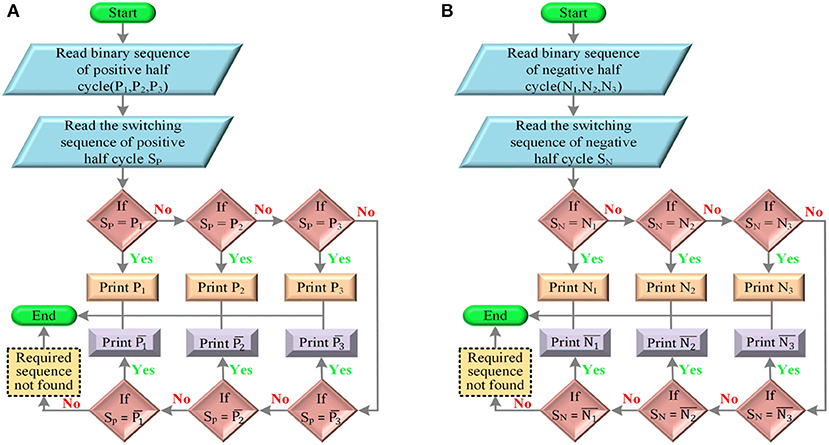
Figure 4. Flowchart for selecting the single-variable pulse sequence. (A) Positive switching sequence. (B) Negative switching sequence.
In combinational two-pulse sequence variable logical operator comparison of switching sequence, positive half switching sequence and negative half switching sequence are individually performed. Various logical operators like AND (•), OR (+), NOR (), NAND , EXOR (⊕), and EXNOR (⊙) are used for the comparative analysis of two variables. Selection of required positive half pulse sequence with two variables for the positive switching sequence is shown in Figure 5A. Similarly, negative half cycle switching sequence comparison with two pulse variables is shown in Figure 5B. From the obtained pulse sequence of positive and negative half pulse variables, the final required switching sequence can be analyzed with the logical operator as shown in Figure 6. Resultants of each switch switching sequence (S#) of various RSMLI are presented as logical expression for the successful operation to generate seven-level output voltage where # is the switch number like S1, S2, S3, etc., in various RSMLIs. Analysis of individual switch in RSMLI, DCL MLI, and SCSD MLI is performed for the logical expression of each switch. Random selections of switching sequence selection operation are presented in tabular analysis.
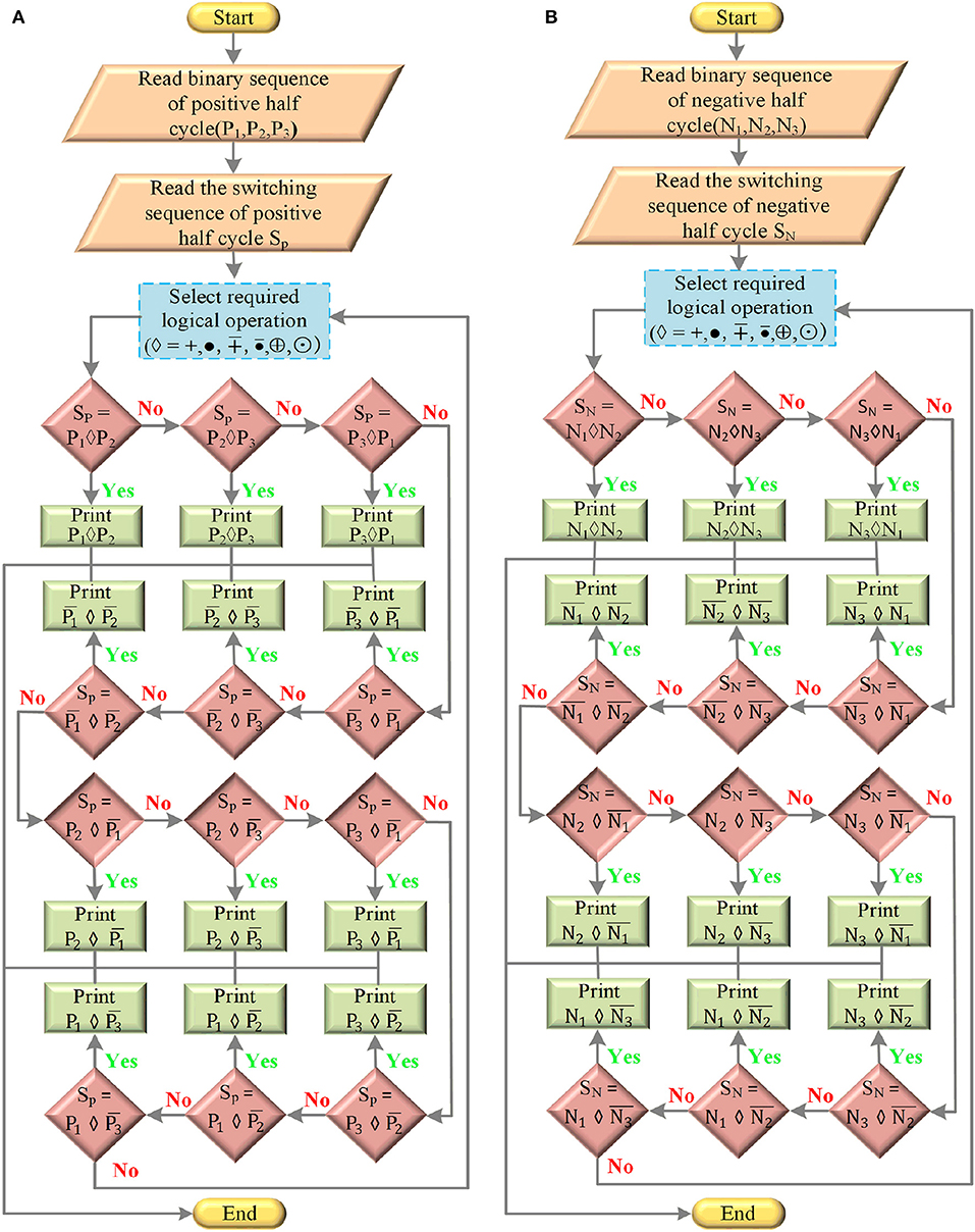
Figure 5. Flowchart for selecting the two-variable pulse sequence. (A) Positive switching sequence. (B) Negative switching sequence.
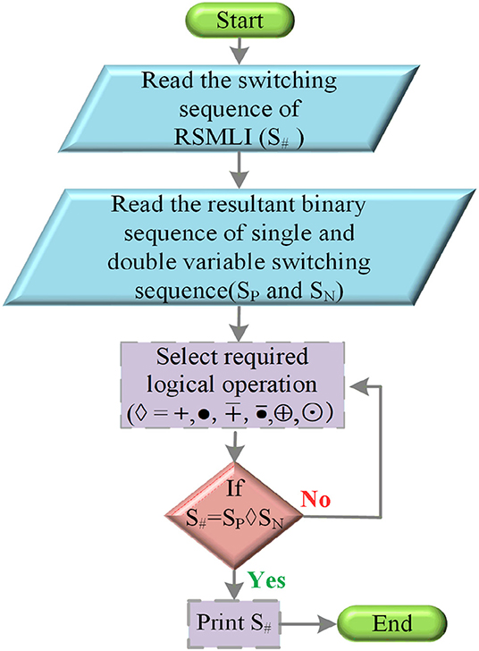
Figure 6. Flowchart for selecting the required logical operation for switching sequence.
Results and THD Comparison
The proposed topology is analyzed for three different RSMLIs and the theoretical analysis of switching sequence logical equations is obtained. To verify the proposed theoretical analysis, MATLAB/Simulink is used for simulation process. Simulation parameters of the three MLIs are given in Table 3. Analysis of proposed methodology to the application of RSMLI, DCL MLI, and SCSD MLI is explained in the below subsections. THD comparison for the obtained output voltage and output current for resistive load of three MLIs with considered modulation techniques are presented.
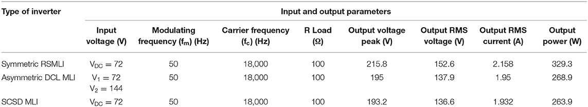
Table 3. Parameters of various RSMLIs.
To generate the modulation wave by the modulation technique, sinusoidal wave is selected for bipolar modulation technique as shown in Figures B1, B3, B4. Absolute sine wave is selected for unipolar modulation technique as shown in Figures B2, B5 with an amplitude of 3 V and a frequency of 50 Hz. Multi-carrier waves are required for the operation of the multi-carrier PWM method as shown in Figures B1–B5. Each carrier wave of multi-carrier PWM is generated with a repeating sequence of the simulink library. Time value parameters of the repeating sequence for carrier waves P1, P2, P3, N1, N2, and N3 are given as [0 0.5/18,000 1/18,000], where 18,000 is the selected switching frequency of the proposed methodology. With respect to the time values of carrier waves, the output amplitude values are selected as [0 1 0] for P1, [2 1 2] for P2, [2 3 2] for P3, [0 −1 0] for N1, [−2 −1 −2] for N2, and [−2 −3 −2] for N3 in the modulation technique of APOD bipolar PWM method as shown in Figure B1; [0 1 0] for P1, [1 2 1] for P2, [2 3 2] for P3, [0 −1 0] for N1, [−1 −2 −1] for N2, and [−2 −3 −2] for N3 in the modulation technique of bipolar POD PWM modulation as shown in Figure B3; [0 1 0] for P1, [1 2 1] for P2, [2 3 2] for P3, [−1 0 −1] for N1, [−2 −1 −2] for N2, and [−3 −2 −3] for N3 in bipolar PD PWM modulation technique as shown in Figure B4; [0 1 0] for P1, [2 1 2] for P2, and [2 3 2] for P3 in unipolar APOD PWM modulation as shown in Figure B2; [0 1 0] for P1, [1 2 1] for P2, and [2 3 2] for P3 in unipolar PD PWM modulation as shown in Figure B5. Greater than relational operator is used in between modulation and carrier wave to obtain required pulse waveforms to switch ON and OFF semiconductor devices in MLIs. Obtained pulse sequences are presented as binary representation in Tables B1, B2. With analysis of proposed methodology between binary representation of pulse sequence and the switching sequence of each switch, the required logical equation for switching sequence is presented in subsections.
Analysis of Proposed Methodology for RSMLI Switching Sequence Logical Equation
An MLI with less number of switches without H bridge is shown in Figure 1A. Five MOSFETs are used for the design and simulation of the RSMLI. Among five switches, three switches are operated for the level generation of output voltage and two are used for the positive half cycle and negative half cycle of output voltage. Four symmetrical voltage sources (VDC) are used for the seven-step MLI output voltage. Each voltage is fixed with a DC voltage of 72 V. Resistive load of 100 Ω is used for the observation of output voltage and current. To operate the switches in the required switching sequence as shown in Table A1, the proposed methodology is applied for the generated pulse sequence of PWM techniques. Focusing on the switching sequence of switch S2, analysis of the proposed methodology is used to obtain logical equation to convert the generated pulse sequence into switching sequence for switch ON and OFF conditions.
The switching sequence of switch S2 is considered as two parts, one is positive half cycle Sp and the other is negative half cycle SN. Bipolar PWM technique is used for the operation of switches in RSMLI. Binary representation of bipolar PWM technique shown in Table B2 is considered for the logical comparative analysis of the proposed methodology. Initially, SP sequence is compared with each binary representation sequence of P1, P2, P3, , , and as shown in Figure 4A. Similarly, SN is compared with each binary representation sequence of N1, N2, N3, , , and as shown in Figure 4B. The pulse sequence matches any of the single-carrier wave pulse sequence; next, focus on the two carrier wave pulse sequence with the combination of logical operators. SP is compared with the combination logical operations of two binary pulse sequence representations as shown in Figure 5A. Logical combination of matches with SP. Similarly, SN is compared with the logical combination of two binary pulse sequence representations as shown in Figure 5B. Logical combination of matches with SN. Total switching sequence of switch S2 is compared with the combination of logical operators of obtained SP and SN as shown in Figure 6. Total binary representation and logical comparison of each stage of switch S2 is given in Table C1. Final logical equation required for the switch S2 operation is obtained and given in Equation (7). With the similar application of proposed methodology, required final logical equations for the switch S1, S3 are presented in Equation (7). Switching sequence of switches S4 and S5 is operated with the pulse sequence of zero reference wave and is given in Equation (7). The resultant pulse sequence of RSMLI obtained with the analysis and the logical equations of each switch is shown in Figure 7.
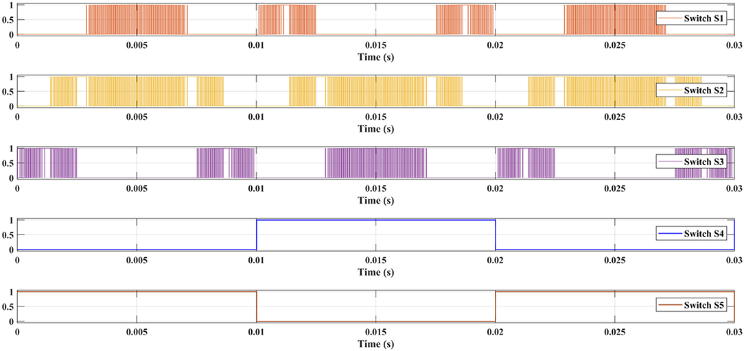
Figure 7. Pulse sequence of RSMLI.
Analysis of Proposed Methodology for DCL MLI Switching Sequence Logical Equation
Asymmetric DC link MLI is simulated with eight MOSFETs as shown in Figure 1B. Four switches are used for the level generation of output voltage and the remaining four switches are used for H bridge to form positive half and negative half cycles. Different voltage sources VDC1 with 72 V and VDC2 with 144 V are used along with a resistive load of 100 Ω. Proposed methodology is applied for the switching sequence of DCL MLI shown in Table A2. Switching sequence operation of switch S6 is presented with analysis of the proposed methodology.
Switching sequences of the switch S1 and S2 of H bridge are operated with zero reference wave pulse sequence PN0. S3 and S4 are operated with pulse sequence of . Similar to RSMLI, Sp and SN are considered and compared with the binary sequence representation of bipolar PWM technique. SP is partially matched with the two pulse sequence logical combination of “P1 ⊕ P2.” Obtained partial match of SP is compared with the single pulse sequence P3 and finds the match of SP results to the logical combination of “(P1 ⊕ P2) ⊕ P3.” SN is partially matched with logical combination of two pulse sequences as “N1 ⊕ N2.” Obtained partial match of SN is logically compared with single pulse sequence N3 and obtained an equivalent as “(N1 ⊕ N2) ⊕ N3.” Overall switching sequence of switch S6 is obtained with the logical combination of the SP and SN as shown in Equation (8). Total binary representation and logical comparisons of each stage of switch S6 are given in Table C2. Switching sequence logical equation for switches S5, S7, and S8 are given in Equation (8) with the analysis of the proposed methodology. The resultant pulse sequence of DCL MLI obtained with the analysis and the logical equations of each switch are shown in Figure 8.
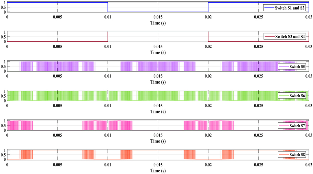
Figure 8. Pulse sequence of DCL MLI.
Analysis of Proposed Methodology for SCSD MLI Switching Sequence Logical Equation
Symmetric Cascaded Switch Diode MLI is simulated with seven MOSFETs and three diodes. Four MOSFETs are used for the H bridge, and three MOSFETs and three diodes are used for the level build process of the SCSD MLI as shown in Figure 1C. Three symmetric voltage sources (VDC) each of 72 V are used for the generation of seven-level output voltage across a resistive load of 100 Ω. Switching sequence of the SCSD MLI is shown in Table A3. Switching sequence of operation of the SCSD MLI is performed with the unipolar PWM technique.
Binary pulse sequence representation of each carrier wave in unipolar PWM technique is presented in Table B1. Switching sequence operation of SCSD MLI is simple as compared with DCL MLI and RSMLI. S1 and S2 switch sequence are matching with the pulse sequence of P0. Switches S3 and S4 sequences are matching with the zero reference wave pulse representation P0. Switches S5, S6, and S7 are directly operated with pulse sequences P1, P2, and P3 as shown in Eq. 9. Binary representation of switching sequence operation of switch S7 is given in Table C3. The resultant pulse sequence of SCSD MLI obtained with the analysis and the logical equations of each switch are shown in Figure 9.
Figure 9. Pulse sequence of DCL MLI.
THD Comparison of MLIs by Proposed Methodology With APOD, POD, and PD Modulation Techniques
By applying the logical equations to the respective switches of RSMLIs, proper seven-level output voltage can be obtained. Input parameters of considered RSMLIs are given in Table 3 with resultant output voltage, RMS output voltage, RMS current, and output power. THD analysis of seven-level output voltage of symmetric RSMLI without H bridge, SCSD RSMLI with bridge, and asymmetric DCL MLI is presented. The obtained THD values of RSMLIs are within the standards. Comparative studies of obtained THD values are given for APOD, POD, and PD PWM techniques with respect to various modulation index values. Voltage THD analysis of APOD, POD, and PD PWM techniques is given in Table 4.
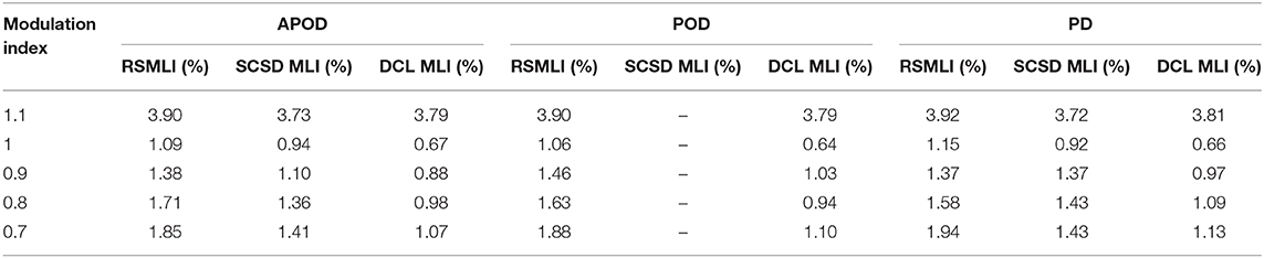
Table 4. Voltage THD comparison of RSMLIs with PWM techniques.
The obtained seven-level output voltage waveform and the FFT analysis of symmetric RSMLI voltage with various PWM methods are shown in Figure D1 with a modulation index of 0.9. Similarly, the obtained seven-level output voltage waveform and FFT analysis of asymmetric DCL MLI and SCSD MLI are shown in Figures D2, D3. Comparative THD analysis is presented for over-modulation index and under-modulation index values in the comparative tables. With the proposed methodology, a lower THD value is obtained with the modulation index value of “1.” Among the three MLIs, DCL MLI is performing well with less THD value of 0.67% by APOD PWM, 0.64% by POD PWM, and 0.66% by PD PWM with a modulation index value of “1.”
Conclusion
This paper presents a new analysis of switching sequence operation for various symmetric and asymmetric RSMLIs with logical operators. A comparative study and observation between various published research articles is presented, and the proposed methodology provides simple analysis and better performance parameters than the previous analysis, by analyzing the pulse sequences of bipolar PWM and unipolar PWM techniques as binary representation and comparing each switching sequence of RSMLI with it. A step-by-step analysis is clearly presented with the calculation of number of carrier waves and modulation techniques. Operational analysis of individual switch is properly presented with the flowchart representations for considered RSMLI, DCL MLI, and SCSD MLI. The resultant logical equation of each switch for various RSMLIs is obtained with the application of the proposed method. Comparative analysis of voltage and current THD values is given without deviating the standards of MLI. The proposed method is suitable for generation of gating signals of various RSMLIs with different PWM methods and can be operated as switch sequence order.
Data Availability Statement
The raw data supporting the conclusions of this article will be made available by the authors, without undue reservation, to any qualified researcher.
Author Contributions
VK contributed for analysis of the switching sequence of RSMLIs and wrote the first draft of the manuscript. SR is the corresponding author and takes primary responsibility for communication with the journal and editorial office during the submission process, throughout peer review and during publication. All authors contributed to manuscript revision, read and approved the submitted version.
Conflict of Interest
The authors declare that the research was conducted in the absence of any commercial or financial relationships that could be construed as a potential conflict of interest.
Supplementary Material
The Supplementary Material for this article can be found online at: https://www.frontiersin.org/articles/10.3389/fenrg.2019.00164/full#supplementary-material
References
Ali, J. S. M., and Kannan, R. (2015). A new symmetric cascaded multilevel inverter topology using single and double source unit. J. Power Electr. 15, 951–963. doi: 10.6113/JPE.2015.15.4.951
Carrara, G., Gardella, S., Marchesoni, M., Salutari, R., and Sciutto, G. (1992). A new multilevel PWM method: a theoretical analysis. IEEE Trans. Power Electron. 7, 497–505. doi: 10.1109/63.145137
Chen, J., Wang, C., and Li, J. (2019). Single-phase step-up five-level inverter with phase-shifted pulse width modulation. J. Power Electron. 19, 134–145. doi: 10.6113/JPE.2019.19.1.134
Chitra, A., and Himavathi, S. (2015). Reduced switch multilevel inverter for performance enhancement of induction motor drive with intelligent rotor resistance estimator. IET Power Electron. 8, 2444–2453. doi: 10.1049/iet-pel.2014.0648
Colak, I., Kabalci, E., and Bayindir, R. (2011). Review of multilevel voltage source inverter topologies and control schemes. Energy Convers. Manage. 52, 1114–1128. doi: 10.1016/j.enconman.2010.09.006
Dong, X., Yu, X., Yuan, Z., Xia, Y., and Li, Y. (2016). An improved SPWM strategy to reduce switching in cascaded multilevel inverters. J. Power Electron. 16, 490–497. doi: 10.6113/JPE.2016.16.2.490
Dorahaki, S. (2015). Evaluating the radiation and temperature effect on photovoltaic systems. Bull. Electr. Eng. Informatics 4, 1–6. doi: 10.11591/eei.v4i1.305
Dorahaki, S., Rashidinejad, M., Mollahassani-pour, M., and Bakhshai, A. (2019). An efficient hybrid structure to solve economic-environmental energy scheduling integrated with demand side management programs. Electr. Eng. 101, 1249–1260. doi: 10.1007/s00202-019-00866-x
Gautam, S. P., Kumar, L., and Gupta, S. (2015). Hybrid topology of symmetrical multilevel inverter using less number of devices. IET Power Electron. 8, 2125–2135. doi: 10.1049/iet-pel.2015.0037
Gnana Prakash, M., Balamurugan, M., and Umashankar, S. (2014). A new multilevel inverter with reduced number of switches. Int. J. Power Electron. Drive System 5, 63–70. doi: 10.11591/ijpeds.v5i1.6089
Gopalakrishnan, K. S., and Narayanan, G. (2014). Space vector based modulation scheme for reducing capacitor RMS current in three-level diode-clamped inverter. Electric Power Syst. Res. 117, 1–13. doi: 10.1016/j.epsr.2014.06.025
Hamman, J., and van der Merwe, F. S. (1988). Voltage harmonics generated by voltage-fed inverters using PWM natural sampling. IEEE Trans. Power Electron. 3, 297–302. doi: 10.1109/63.17947
Hava, A. M., Kerkman, R. J., and Lipo, T. A. (1999). Simple analytical and graphical methods for carrier-based PWM-VSI drives. IEEE Trans. Power Electron. 14, 49–61. doi: 10.1109/63.737592
Holtz, J. (1992). Pulsewidth modulation—a survey. IEEE Trans. Indus. Electron. 39, 410–420. doi: 10.1109/41.161472
Huang, J., Liu, Q., Wang, X., and Li, K. (2018). A carrier-based modulation scheme to reduce the third harmonic component of common-mode voltage in a three-phase inverter under high DC voltage utilization. IEEE Trans. Indus. Electron. 65, 1931–1940. doi: 10.1109/TIE.2017.2745439
Krishna, M. D., and Vadhera, S. (2013). Comparative study of hybrid and cascaded h-bridge multilevel inverters. Int. J. Res. Eng. Technol. 405–10. doi: 10.15623/ijret.2013.0208063
Kumar, K. V., and Kumar, S. R. (2018). Advanced PWM techniques for control of power electronic converters in PV and motor drive systems. Int. J. Pure Appl. Math. 118, 1–21.
Kumar, K. V., and Kumar, S. R. (2019a). Analysis of logic gates for generation of switching sequence in symmetric and asymmetric reduced switch multilevel inverter. IEEE Access 7, 97719–97731. doi: 10.1109/ACCESS.2019.2929836
Kumar, K. V., and Kumar, S. R. (2019b). Switching sequence control of reduced switch count multilevel inverter with multi carrier pulse width modulation. Int. J. Sci. Technol. Res. 8, 3790–3798.
McGrath, B. P., and Holmes, D. G. (2002). Multicarrier PWM strategies for multilevel inverters. IEEE Trans. Indus. Electron. 49, 858–867. doi: 10.1109/TIE.2002.801073
Nagarajan, R., and Saravanan, M. (2014). Performance analysis of a novel reduced switch cascaded multilevel inverter. J. Power Electron. 14, 48–60. doi: 10.6113/JPE.2014.14.1.48
Narendiran, S., and Sahoo, S. K. (2017). A single phase reduced device count multilevel inverter topology using MCPWM for renewable energy systems. Energy Procedia 117, 1–8. doi: 10.1016/j.egypro.2017.05.128
Orfi Yegane, M. S., and Sarvi, M. (2018). An improved harmonic injection PWM-frequency modulated triangular carrier method with multiobjective optimizations for inverters. Electric Power Syst. Res. 160, 372–380. doi: 10.1016/j.epsr.2018.03.011
Prabaharan, N., and Palanisamy, K. (2016). Comparative analysis of symmetric and asymmetric reduced switch MLI topologies using unipolar pulse width modulation strategies. IET Power Electron. 9, 2808–2823. doi: 10.1049/iet-pel.2016.0283
Prabaharan, N., and Palanisamy, K. (2017). A comprehensive review on reduced switch multilevel inverter topologies, modulation techniques and applications. Renew. Sustain. Energy Rev. 76, 1248–1282. doi: 10.1016/j.rser.2017.03.121
Prasad, G. D., Jegathesan, V., and Rama Rao, P. V. V. (2017). Hybrid multilevel DC link inverter with reduced power electronic switches. Energy Procedia 117, 626–634. doi: 10.1016/j.egypro.2017.05.162
Sudhakar Babu, T., Priya, K., Maheswaran, D., Sathish Kumar, K., and Rajasekar, N. (2015). Selective voltage harmonic elimination in PWM inverter using bacterial foraging algorithm. Swarm Evolut. Comput. 20, 74–81. doi: 10.1016/j.swevo.2014.11.002
Umashankar, S., Sreedevi, T. S., Nithya, V. G., and Vijayakumar, D. (2013). A new 7-level symmetric multilevel inverter with minimum number of switches. ISRN Electron. 2013:9. doi: 10.1155/2013/476876
Uthirasamy, R., Ragupathy, U. S., and Kumar, V. (2015). Structure of boost DC-link cascaded multilevel inverter for uninterrupted power supply applications. IET Power Electron. 8, 2085–2096. doi: 10.1049/iet-pel.2014.0746
Vemuganti, H. P., Sreenivasarao, D., Siva Kumar, G., and Sai Spandana, A. (2018). Reduced carrier PWM scheme with unified logical expressions for reduced switch count multilevel inverters. IET Power Electron. 11, 912–921. doi: 10.1049/iet-pel.2017.0586
Keywords: pulse width modulation, multilevel inverter, reduced switch multilevel inverter, switching sequence, logic gates, total harmonic distortion
Citation: Kanike VK and Raju S (2020) Analysis of Switching Sequence Operation for Reduced Switch Multilevel Inverter With Various Pulse Width Modulation Methods. Front. Energy Res. 7:164. doi: 10.3389/fenrg.2019.00164
Received: 29 November 2019; Accepted: 23 December 2019;
Published: 28 January 2020.
Edited by:
Sam Sichilalu, University of Zambia, ZambiaReviewed by:
Marif Daula Siddique, University of Malaya, MalaysiaSobhan Dorahaki, Shahid Bahonar University of Kerman, Iran
Copyright © 2020 Kanike and Raju. This is an open-access article distributed under the terms of the Creative Commons Attribution License (CC BY). The use, distribution or reproduction in other forums is permitted, provided the original author(s) and the copyright owner(s) are credited and that the original publication in this journal is cited, in accordance with accepted academic practice. No use, distribution or reproduction is permitted which does not comply with these terms.
*Correspondence: Saravanakumar Raju, cnNhcmF2YW5ha3VtYXJAdml0LmFjLmlu