 Khaled Humood
 Yihan Pan
 Shiwei Wang
 Alexander Serb
 Themis Prodromakis
- The Centre for Electronics Frontiers, Institute for Integrated Micro and Nano Systems, School of Engineering, University of Edinburgh, Edinburgh, United Kingdom
Recently, there has been notable progress in the advancement of RRAM-based Compute-In-Memory (CIM) architectures, showing promise in accelerating neural networks with remarkable energy efficiency and parallelism. However, challenges persist in fully integrating large-scale networks onto a chip, particularly when the weights of a layer exceed the capacity of the RRAM crossbar. In such cases, weights are distributed across smaller RRAM crossbars and aggregated using tree adders and shifters in digital flow, leading to increased system complexity and energy consumption of hardware accelerators. In this work, we introduce a novel energy-efficient analog domain aggregator system designed for RRAM-based CIM systems. The proposed circuit has been verified and tested using Virtuoso Cadence circuit tools in 180 nm CMOS technology with post-layout simulations and analysis. Compared with the digital adder tree approach, the proposed analog aggregator offers improvements in three key areas: it can handle an arbitrary number of inputs not just powers of 2, achieves lower error through better rounding and improves power efficiency (2.15
1 Introduction
The deployment of neural networks (NNs) in machine learning (ML) applications, including computer vision, speech recognition, and natural language processing, has grown exponentially over the past few decades (Hertel et al., 2015; Graves et al., 2013; Bahdanau et al., 2015; Humood et al., 2023). To address the intensive Multiply-Accumulate (MAC) operations required by these applications, emerging circuit architectures such as Compute-In-Memory (CIM) modules have been developed (Yu et al., 2021). Resistive Random Access Memory (RRAM)-based neural network (NN) accelerators (Musisi-Nkambwe et al., 2021; Mittal, 2019; Yao et al., 2020; Marinella et al., 2018; Cai et al., 2019; Bayat et al., 2018; Sahay et al., 2020; Liu et al., 2020; Mochida et al., 2018; Shafiee et al., 2016; Xue et al., 2020; Prezioso et al., 2018; Ankit et al., 2017; Wang et al., 2015; Narayanan et al., 2017; Hung et al., 2021; Tang et al., 2017; Ming et al., 2017; Chen et al., 2019; Su et al., 2017; Wang et al., 2024) have attracted considerable attention due to their utilization of Ohm’s law for multiplication and Kirchhoff’s law for accumulation. By leveraging an RRAM array, these engines can execute parallel in-memory MAC operations, offering substantially enhanced speed and energy efficiency compared to von Neumann computing approaches (Amirsoleimani et al., 2020; Mittal, 2019).
However, despite recent advances in RRAM-based accelerators, there remain several challenges at the system level that need to be addressed in order to effectively implement large-scale NNs, such as AlexNet (Krizhevsky et al., 2017), VGG-16 (Simonyan and Zisserman, 2015), and ResNet (He et al., 2016) on chip. A notable challenge arises when the necessary fan-in within an NN exceeds the capacity of the RRAM crossbar, limiting hardware implementability of large-scale networks (the “aggregation problem”). Simply increasing the size of the RRAM crossbar is not an efficient solution due to constraints related to write/read errors (Yuan et al., 2019), sneak path currents (Humood et al., 2019), and latency (Xia et al., 2018), which tend to worsen with larger array sizes.
Instead, the ISAAC architecture reported in (Shafiee et al., 2016) distributes the weights of large NNs across multiple RRAM arrays to execute partial sum product computation quickly and in parallel (Huo et al., 2022). Subsequently, the outputs from each array on the same column are aggregated/accumulated using adder trees and shifters in the digital domain before being transmitted to the next layer or output registers. Several other architectures have also adopted similar adder tree- and shifter-based approaches, (Yuan et al., 2019; Wang et al., 2021; Xia et al., 2018; Zhang et al., 2019; Chi et al., 2016; Nag et al., 2018; Yao et al., 2020; Wang et al., 2023). Other research efforts have implemented aggregation on FPGAs (Liu et al., 2020; Hung et al., 2021; 2023; Huo et al., 2022), however, this limits the concept of having a full system on chip.
However, the aforementioned studies do not address the performance and implementation of the aggregation system, hence, the practical overhead of accumulating inputs from different crossbars at the system level remains unknown. Additionally, the digital approach using adder trees and shifters can only accumulate outputs from
In this work, we present a novel analog-domain aggregator circuit for RRAM-based accelerators. The proposed circuit is designed to accumulate the digital outputs of N number of sub-arrays within the hardware NN accelerators via charge redistribution/sharing techniques. First, the digital output of each array on the same column is converted from the digital domain to the analog domain through C-2C DAC ladders. Subsequently, the analog outputs of the C-2C ladders are accumulated and shared across a single line. Finally, the aggregated analog signal is converted back to the digital domain using a SAR ADC to be processed for the next NN layer or to the output registers. Furthermore, considering that most NNs generate signed outputs, positive and negative sub-array outputs are individually accumulated and subsequently subtracted from each other during the aggregation process. Figure 1 shows the proposed approach along with other approaches in the literature for “aggregators” used in RRAM-based NN accelerators.
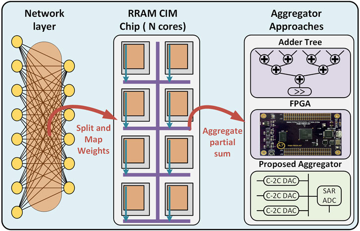
Figure 1. Mapping a large-scale neural network on multi-core RRAM CIM chip. To the right, we illustrate the proposed approach to aggregate partial sums (green outline) along with Adder Tree (Yuan et al., 2019; Wang et al., 2021; Xia et al., 2018; Zhang et al., 2019; Chi et al., 2016; Nag et al., 2018; Yao et al., 2020; Wang et al., 2023) and FPGA (Liu et al., 2020; Hung et al., 2021; 2023; Huo et al., 2022) approaches.
The proposed aggregator is validated via Cadence Virtuoso in a commercially available 180 nm CMOS technology. Post-layout simulation and analysis have been performed to evaluate the circuit’s performance and characteristics. To validate the performance of the proposed system, we also implemented and simulated the adder tree and shifter system utilized in ISAAC (Shafiee et al., 2016) using digital Register Transfer Level (RTL) methodology on Application Specific Integrated Circuits (ASIC) design flow, providing a direct comparison vs. a fully digital approach. Results demonstrate improved flexibility, precision and power performance of the proposed analog aggregator. The demonstrated aggregator version is capable of accumulating outputs from up to 8 different arrays, which is sufficient to accommodate the majority of large RRAM-based NN accelerators such as ISAAC (4 arrays per bank) (Shafiee et al., 2016) and PRIME (8 arrays per bank) (Chi et al., 2016). However, expanding the number of digital outputs that the proposed aggregator can accumulate is easily achieved by increasing the number of C-2C DAC ladders. To the best of our knowledge, we are the first to successfully demonstrate the design of an analog domain aggregator specifically tailored for CIM architectures.
The remainder of this paper is organized as follows: Section 2 provides an overview of the proposed aggregator architecture. Section 3 describes the methodology of the charge-sharing operation and analog sharing mechanism and the transition of the signal from input to output along with design constraints and design parameters. Simulation results and performance evaluation are provided in Section 4, followed by conclusions in Section 5.
2 System overview and methodology
The proposed aggregator schematic and layout are shown in Figures 2A, B, respectively. This section discusses the mode of operation and circuit design, including the exploration of design parameters and system specifications.
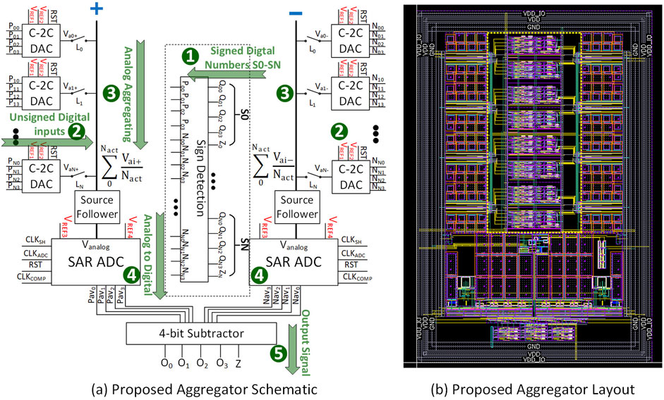
Figure 2. Proposed aggregator architecture. (A) Schematic view. See text for description of signal flow steps (numbers in green). (B) Layout view (
2.1 Mode of operation and charge sharing
The numbers and arrows in Figure 2A denote the signal flow. Given that the outputs of a neural network layer can vary in sign, the outputs of an RRAM-based accelerator are represented as a signed digital number (S). Step 1: 5-bit, signed digital numbers (
This aggregator can accumulate up to 8 digital numbers but expanding to in principle arbitrary numbers of input blocks is easily achieved by increasing the number of C-2C DAC units (not just powers of 2). This results directly from the nature of charge-sharing, where every contributor is implicitly equally weighted, thus enhancing versatility vs. conventional digital aggregation techniques. Each DAC unit is equipped with a switch
2.2 System overview
2.2.1 Sign detection
The sign detection block utilized in this study is shown in Figure 3. It receives a 5-bit digital number (
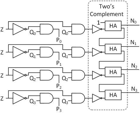
Figure 3. Sign detection circuit used in the proposed Aggregator. HA, Half-Adder.
2.2.2 C-2C DAC
In this work, the digital-to-analog conversion at the input side is performed using a modified version of the textbook C-2C DAC circuit (Singh et al., 1987). A C-2C DAC is a data converter that uses a binary-weighted capacitor network to convert digital inputs into analog voltages. The name “C-2C” refers to its use of unit (C) and double unit (2C) capacitances. Two DAC ladders are employed, one for the positive aggregating side and one for the negative side. Figure 4 displays a single DAC unit from the positive aggregating side, with a corresponding DAC unit implemented on the negative aggregating side. The value of C is minimized to 100 fF to reduce area and power while maintaining good linearity and minimizing the effect of parasitic capacitances. The RST signal resets the analog line to 0 V before the start of the conversion. The positive equivalent numbers are transformed into an analog voltage represented as
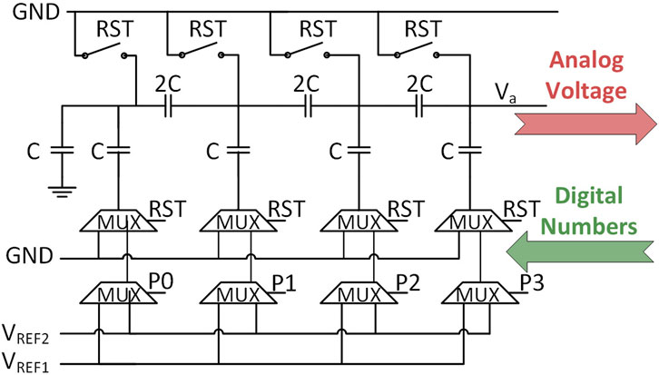
Figure 4. C-2C DAC Unit Used on the Positive Side of the Proposed Aggregator, with an Identical Unit Implemented on the Negative Side. Capacitance Value (C) is 100 fF.
2.2.3 SAR ADC
The SAR-ADC circuit, referenced in (Sharuddin et al., 2016; Alpman et al., 2009) and illustrated in Figure 5, constitutes the largest component within the proposed aggregator. The implemented SAR-ADC consists of 4 main components. First, the sample and hold circuit (S/H), as shown in the inset of Figure 5, is used to sample and hold the analog voltage obtained from the averaging DAC ladders when
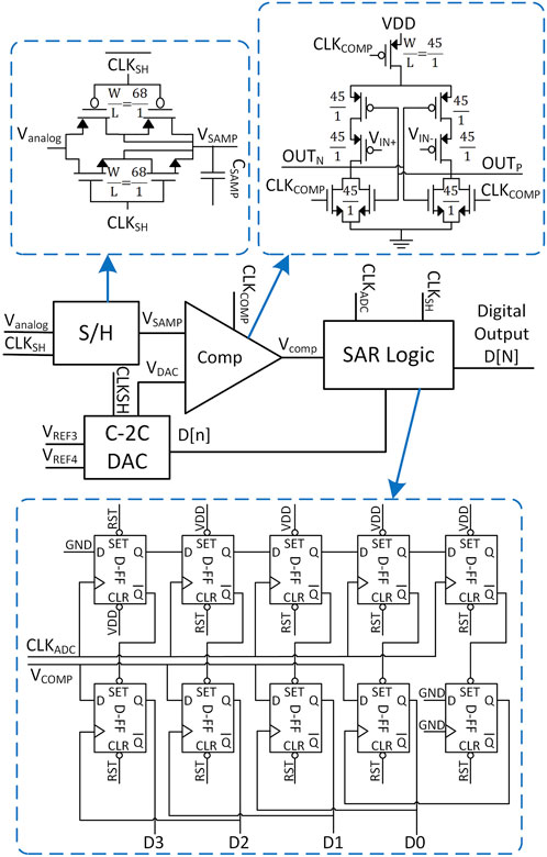
Figure 5. SAR-ADC design utilized in the proposed aggregator. Also shown: schematics of the sample and hold circuit, the comparator, and the SAR logic.
Second, The comparator employed in the implemented SAR-ADC is based on the strong-ARM latch comparator reported in (Almansouri et al., 2017; Kobayashi et al., 1993) due to their low offset, low power consumption, and high input impedance. The comparator is needed to compare the analog sampled value with the DAC output. In order to operate at a low common-mode voltage, a PMOS-input latch comparator is used in this work. The comparator design, along with the width-to-length ratio of the transistors, is shown in the inset of Figure 5. Transistors were sized to minimize the offset, as evidenced by post-layout Monte Carlo simulations demonstrating an offset of less than 5 mV at a common-mode voltage of 0.1 V.
Third, The SAR logic shown in the inset of Figure 5 is implemented using two shift registers composed of chains of standard D-Flip Flops (D-FFs). The shift register at the top serves as a sequencer and operates synchronously with the internal clock. Meanwhile, the bottom register stores the conversion value. The final component of the SAR ADC is the C-2C DAC unit, as described earlier in Section 2.2.2 and depicted in Figure 4. However, the value of C in this C-2C DAC is set to 720 fF to minimize kickback noise from the strong-ARM latch comparator.
2.2.4 4-bit subtractor
This is used to subtract the negative aggregated output from the positive aggregated output, here a standard 4-bit subtractor unit. Its output represents the final digital result of the accumulation process.
2.3 Design parameters
In the proposed aggregator, there are four design parameters, namely,
Figure 6 provides a graphical representation of the balancing process, illustrating the signal range transition from input to output. As the averaging DAC ladder is connected to an NMOS-based source follower before going to SAR ADC block,
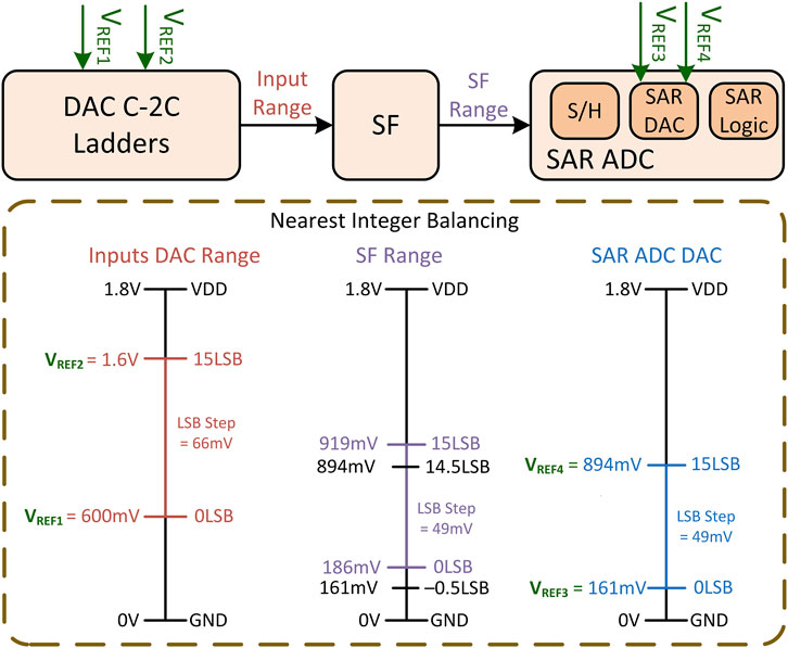
Figure 6. Aggregator
3 Results
The proposed aggregator circuit has been validated in Cadence via post-layout simulations at 180 nm commercial CMOS and under a 1.8 V power supply.
3.1 Post layout transient simulation
Figure 7 presents a SPICE post-layout simulation of the proposed circuit using a randomized set of 8-signed digital inputs (
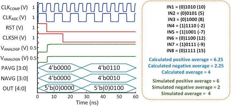
Figure 7. Example of post-layout simulation of the proposed aggregator system using a randomized set of 8-signed digital inputs.
3.2 Corner and temp analysis
Table 1 presents a summary of the process corner and temperature analysis across three different process corners (nmos-pmos) and five temperatures (ranging from −55°C to 125°C). The analysis is based on the simulation of three randomized digital input combinations. Table 1 shows the LSB deviation between the simulated output and expected output (expected - simulated) for each corner and case. A deviation of 0 LSB indicates a correct conversion, highlighted in green in the table. Red-highlighted cells indicate incorrect conversions, along with the extent to which the simulated output deviates from the expected output. Overall, the system demonstrates excellent performance, passing most corners and only failing in extreme corners with a deviation of only
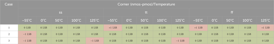
Table 1. Process corner and temperature analysis for different input combinations (Case 1 - Case 3). Table entries: deviation between simulated output and expected output (expected - simulated) in units of LSB.
3.3 Monte Carlo analysis
Monte Carlo analysis and simulations were carried out on the proposed aggregator circuit to examine the influence of transistor mismatch. Figure 8 presents histograms of the aggregated outputs under four randomized sets of digital inputs. The random inputs were chosen to correspond to exact aggregation results of 6, 6.25, 6.5 and 6.75 (decimal), i.e., in 0.25LSB increments (Case 1 - Case 4). Hence, the correct nearest-integer-rounded results would be 6, 6, 7, and 7, respectively. We ran the test 200 times and recorded the results of the aggregation. Results in Figure 8 show the vast majority of trials returning the correct answer (0 LSB error), with Case 3 (exact answer = 6.5, rounded answer = 7) showing the biggest incidence of imprecisions with 6% of total trials resulting in code 6 instead of 7 (Figure 8C). We note that this is a borderline case and as such the absolute error vs. the exact answer is 0.5 LSBs in for both code 6 and 7. Another observation is that the worst error appears in Case 1, where 0.5% of trials result in 1 full LSB difference from the exact answer.
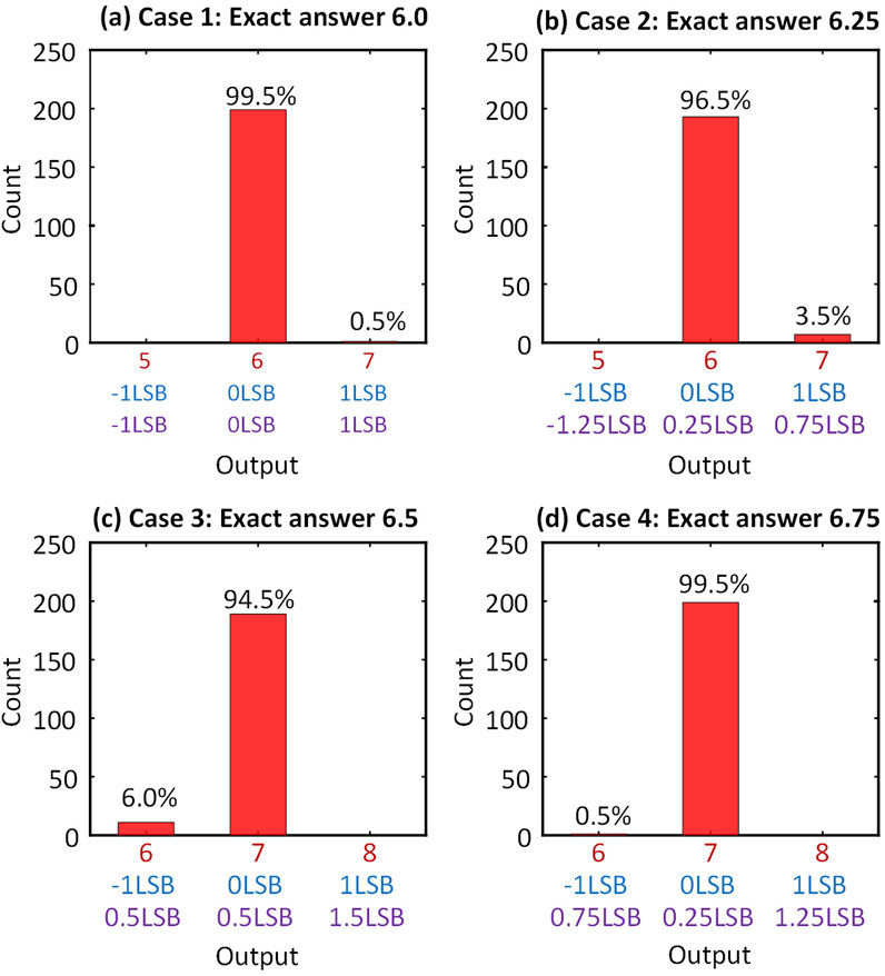
Figure 8. (A-D) Monte Carlo post-layout simulation of the proposed aggregator system using a randomized set of 8-signed digital inputs. X-axis: Top row (red): Rounded output code, i.e., final output of aggregator. Middle row (blue): Deviation from expected output code. Bottom row (purple): Difference of aggregator output code from exact answer. Percentage of each count is shown above each bar.
3.4 Power and area breakdown
Table 2 presents the average power consumption and area breakdown of each component in the proposed aggregator. The metrics in Table 2 are based on post-layout extracted simulation under a random set of digital inputs. The average power consumption was measured while operating at a

Table 2. Proposed Aggregator area and power breakdown.
3.5 Performance comparison with digital approach
Table 3 presents a comparison of performance and specifications between the proposed analog aggregator and the digital adder tree aggregator proposed in (Shafiee et al., 2016; Yuan et al., 2019; Wang et al., 2021; Xia et al., 2018; Zhang et al., 2019; Chi et al., 2016; Nag et al., 2018; Yao et al., 2020). However, the aforementioned studies do not provide details about how a circuit block with the function of digital aggregator might be built or how it might perform. Hence, the digital aggregator has been implemented using an RTL digital flow implementation using the same CMOS technology node, input/output resolution, and number of aggregated inputs of the proposed aggregator. The digital ASIC flow applies standard cells provided by the foundry. Its output loading is set to 50 fF, the same as the analog flow implementation for comparison.
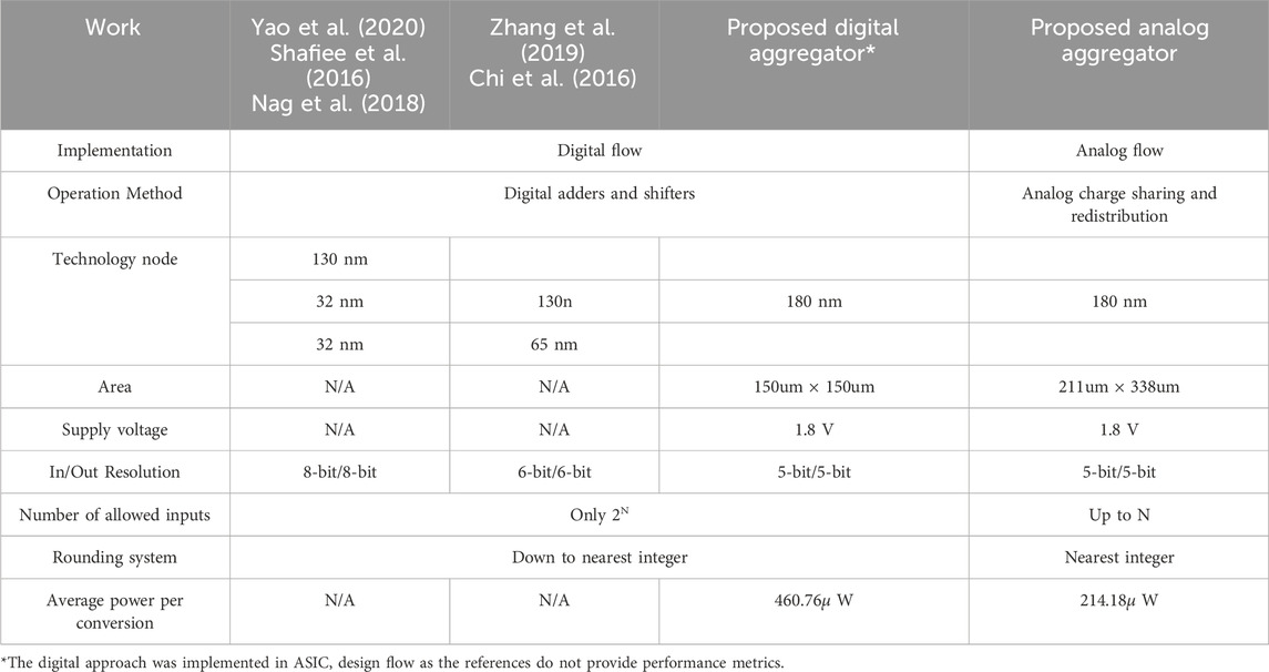
Table 3. Performance comparison and specification summary between the digital and analog implementations of the Aggregator system.
The proposed analog aggregator offers three key advantages over its digital counterpart. Firstly, it can accumulate a higher number of inputs (arbitrary up to N), whereas the digital aggregator is limited to power of 2 inputs due to the limitations of shift operations used to average the sum of inputs. Secondly, the analog aggregator is designed to round the final sum to the nearest integer, reducing the error to 0.5 LSB, while the digital approach rounds down, resulting in “natural” errors up to 1 LSB. Finally, the analog aggregator system demonstrates an improvement of approximately 2.15
4 Conclusion
In this work, we presented a novel energy-efficient analog domain aggregator circuit designed for RRAM-based neural network accelerators. An Aggregator system is needed when the weights of a neural network layer exceed the capacity of the RRAM crossbar. The proposed aggregator is designed to accumulate the digital outputs of the subarrays within the hardware NN accelerators via charge distribution and sharing techniques in analog flow. We implemented and verified the proposed circuit using Cadence circuit tools. The functionality and performance of the system were evaluated through post-layout simulations using a commercially available 180 nm CMOS technology and compared with the digital approach used in the state-of-the-art. The proposed system offers a more flexible design, higher precision (at 5 bits), and improved power consumption compared to the digital approach. While the proposed aggregator design aims to enhance the performance of pipelining in RRAM-based accelerators, the design itself neither incorporates RRAM technology nor is directly influenced by RRAM devices, as the system’s inputs and outputs are in digital format. In fact, the aggregator can be adapted for use with any compute-in-memory technology, such as SRAM-based or DRAM-based CIM.
Data availability statement
The original contributions presented in the study are included in the article/supplementary material, further inquiries can be directed to the corresponding author.
Author contributions
KH: Conceptualization, Investigation, Methodology, Software, Visualization, Writing–original draft, Writing–review and editing. YP: Software, Validation, Writing–review and editing. SW: Supervision, Writing–review and editing. AS: Investigation, Methodology, Supervision, Writing–review and editing. TP: Funding acquisition, Supervision, Writing–review and editing.
Funding
The author(s) declare that financial support was received for the research, authorship, and/or publication of this article. This work was supported by the Engineering and Physical Sciences Research Council (EPSRC) Programme Grant EP/R024642/2 “Functional Oxide Reconfigurable Technologies (FORTE)” and the RAEng Chair in Emerging Technologies (CiET1819/2/93).
Acknowledgments
The authors would like to thank Shady Agwa and Grahame Reynolds for their valuable discussion and support.
Conflict of interest
The authors declare that the research was conducted in the absence of any commercial or financial relationships that could be construed as a potential conflict of interest.
Generative AI statement
The author(s) declare that no Generative AI was used in the creation of this manuscript.
Publisher’s note
All claims expressed in this article are solely those of the authors and do not necessarily represent those of their affiliated organizations, or those of the publisher, the editors and the reviewers. Any product that may be evaluated in this article, or claim that may be made by its manufacturer, is not guaranteed or endorsed by the publisher.
References
Almansouri, A., Alturki, A., Alshehri, A., Al-Attar, T., and Fariborzi, H. (2017). Improved strongarm latch comparator: design, analysis and performance evaluation. 2017 13th Conf. Ph.D. Res. Microelectron. Electron. (PRIME), 89–92. doi:10.1109/PRIME.2017.7974114
Alpman, E., Lakdawala, H., Carley, L. R., and Soumyanath, K. (2009). A 1.1v 50mw 2.5gs/s 7b time-interleaved c-2c sar adc in 45nm lp digital cmos. 2009 IEEE Int. Solid-State Circuits Conf. - Dig. Tech. Pap., 76–77,77a. doi:10.1109/ISSCC.2009.4977315
Amirsoleimani, A., Alibart, F., Yon, V., Xu, J., Pazhouhandeh, M. R., Ecoffey, S., et al. (2020). In-memory vector-matrix multiplication in monolithic complementary metal–oxide–semiconductor-memristor integrated circuits: design choices, challenges, and perspectives. Adv. Intell. Syst. 2, 2000115. doi:10.1002/aisy.202000115
Ankit, A., Sengupta, A., Panda, P., and Roy, K. (2017). “Resparc: a reconfigurable and energy-efficient architecture with memristive crossbars for deep spiking neural networks,” in 2017 54th ACM/EDAC/IEEE Design Automation Conference (DAC), Austin, TX, USA, 1–6.
Bayat, F. M., Prezioso, M., Chakrabarti, B., Nili, H., Kataeva, I., and Strukov, D. (2018). Implementation of multilayer perceptron network with highly uniform passive memristive crossbar circuits. Nat. Commun. 9, 2331. doi:10.1038/s41467-018-04482-4
Cai, F., Correll, J. M., Lee, S. H., Lim, Y., Bothra, V., Zhang, Z., et al. (2019). A fully integrated reprogrammable memristor–cmos system for efficient multiply–accumulate operations. Nat. Electron. 2, 290–299. doi:10.1038/s41928-019-0270-x
Chen, W.-H., Dou, C., Li, K.-X., Lin, W.-Y., Li, P.-Y., Huang, J.-H., et al. (2019). Cmos-integrated memristive non-volatile computing-in-memory for ai edge processors. Nat. Electron. 2, 420–428. doi:10.1038/s41928-019-0288-0
Chi, P., Li, S., Xu, C., Zhang, T., Zhao, J., Liu, Y., et al. (2016). Prime: a novel processing-in-memory architecture for neural network computation in reram-based main memory. 2016 ACM/IEEE 43rd Annu. Int. Symposium Comput. Archit. (ISCA), 27–39. doi:10.1109/ISCA.2016.13
[Dataset] Bahdanau, D., Cho, K., and Bengio, Y. (2015). Neural machine translation by jointly learning to align and translate. arXiv. doi:10.48550/arXiv.1409.0473
[Dataset] Wang, Y., Tang, T., Xia, L., Li, B., Gu, P., Yang, H., et al. (2015). Energy efficient rram spiking neural network for real time classification. Comput. Sci. Eng. doi:10.1145/2742060.2743756
Graves, A., Mohamed, A.-R., and Hinton, G. (2013). Speech recognition with deep recurrent neural networks. IEEE Int. Conf. Acoust. Speech Signal Process., 6645–6649. doi:10.1109/icassp.2013.6638947
He, K., Zhang, X., Ren, S., and Sun, J. (2016). Deep residual learning for image recognition. Proc. IEEE Conf. Comput. Vis. Pattern Recognit. (CVPR). doi:10.1109/CVPR.2016.90
Hertel, L., Barth, E., Käster, T., and Martinetz, T. (2015). Deep convolutional neural networks as generic feature extractors. 2015 Int. Jt. Conf. Neural Netw. (IJCNN), 1–4. doi:10.1109/ijcnn.2015.7280683
Humood, K., Hadi, S. A., Mohammad, B., Jaoude, M. A., Alazzam, A., and Alhawari, M. (2019). High-density reram crossbar with selector device for sneak path reduction. 2019 31st Int. Conf. Microelectron. (ICM), 244–248. doi:10.1109/ICM48031.2019.9021944
Humood, K., Serb, A., Wang, S., and Prodromakis, T. (2023). Quicknn: Python toolbox for training and optimizing ann for hardware implementation. 2023 IEEE 66th Int. Midwest Symposium Circuits Syst. (MWSCAS), 531–535. doi:10.1109/MWSCAS57524.2023.10405963
Hung, J.-M., Wen, T.-H., Huang, Y.-H., Huang, S.-P., Chang, F.-C., Su, C.-I., et al. (2023). 8-b precision 8-mb reram compute-in-memory macro using direct-current-free time-domain readout scheme for ai edge devices. IEEE J. Solid-State Circuits 58, 303–315. doi:10.1109/JSSC.2022.3200515
Hung, J.-M., Xue, C.-X., Kao, H.-Y., Huang, Y.-H., Chang, F.-C., Huang, S.-P., et al. (2021). A four-megabit compute-in-memory macro with eight-bit precision based on cmos and resistive random-access memory for ai edge devices. Nat. Electron. 4, 921–930. doi:10.1038/s41928-021-00676-9
Huo, Q., Yang, Y., Wang, Y., Lei, D., Fu, X., Ren, Q., et al. (2022). A computing-in-memory macro based on three-dimensional resistive random-access memory. Nat. Electron. 5, 469–477. doi:10.1038/s41928-022-00795-x
Kobayashi, T., Nogami, K., Shirotori, T., and Fujimoto, Y. (1993). A current-controlled latch sense amplifier and a static power-saving input buffer for low-power architecture. IEEE J. Solid-State Circuits 28, 523–527. doi:10.1109/4.210039
Krizhevsky, A., Sutskever, I., and Hinton, G. E. (2017). Imagenet classification with deep convolutional neural networks. Commun. ACM 60, 84–90. doi:10.1145/3065386
Liu, Q., Gao, B., Yao, P., Wu, D., Chen, J., Pang, Y., et al. (2020). 33.2 a fully integrated analog reram based 78.4tops/w compute-in-memory chip with fully parallel mac computing. 2020 IEEE Int. Solid- State Circuits Conf. - (ISSCC), 500–502. doi:10.1109/ISSCC19947.2020.9062953
Marinella, M. J., Agarwal, S., Hsia, A., Richter, I., Jacobs-Gedrim, R., Niroula, J., et al. (2018). Multiscale co-design analysis of energy, latency, area, and accuracy of a reram analog neural training accelerator. IEEE J. Emerg. Sel. Top. Circuits Syst. 8, 86–101. doi:10.1109/jetcas.2018.2796379
Ming, C., Lixue, X., Zhenhua, Z., Yi, C., Yuan, X., Yu, W., et al. (2017). Time: a training-in-memory architecture for memristor-based deep neural networks. 2017 54th ACM/EDAC/IEEE Des. Autom. Conf. (DAC), 1–6. doi:10.1145/3061639.3062326
Mittal, S. (2019). A survey of reram-based architectures for processing-in-memory and neural networks. Mach. Learn. Knowl. Extr. 1, 75–114. doi:10.3390/make1010005
Mochida, R., Kouno, K., Hayata, Y., Nakayama, M., Ono, T., Suwa, H., et al. (2018). A 4m synapses integrated analog reram based 66.5 tops/w neural-network processor with cell current controlled writing and flexible network architecture. 2018 IEEE Symposium VLSI Technol., 175–176. doi:10.1109/vlsit.2018.8510676
Musisi-Nkambwe, M., Afshari, S., Barnaby, H., Kozicki, M., and Sanchez Esqueda, I. (2021). The viability of analog-based accelerators for neuromorphic computing: a survey. Neuromorphic Comput. Eng. 1, 012001. doi:10.1088/2634-4386/ac0242
Nag, A., Balasubramonian, R., Srikumar, V., Walker, R., Shafiee, A., Strachan, J. P., et al. (2018). Newton: gravitating towards the physical limits of crossbar acceleration. IEEE Micro 38, 41–49. doi:10.1109/MM.2018.053631140
Narayanan, S., Shafiee, A., and Balasubramonian, R. (2017). Inxs: bridging the throughput and energy gap for spiking neural networks. 2017 Int. Jt. Conf. Neural Netw. (IJCNN), 2451–2459. doi:10.1109/IJCNN.2017.7966154
Prezioso, M., Mahmoodi, M. R., Bayat, F. M., Nili, H., Kim, H., Vincent, A., et al. (2018). Spike-timing-dependent plasticity learning of coincidence detection with passively integrated memristive circuits. Nat. Commun. 9, 5311. doi:10.1038/s41467-018-07757-y
Sahay, S., Bavandpour, M., Mahmoodi, M. R., and Strukov, D. (2020). Energy-efficient moderate precision time-domain mixed-signal vector-by-matrix multiplier exploiting 1t-1r arrays. IEEE J. Explor. Solid-State Comput. Devices Circuits 6, 18–26. doi:10.1109/JXCDC.2020.2981048
Shafiee, A., Nag, A., Muralimanohar, N., Balasubramonian, R., Strachan, J. P., Hu, M., et al. (2016). Isaac: a convolutional neural network accelerator with in-situ analog arithmetic in crossbars. 2016 ACM/IEEE 43rd Annu. Int. Symposium Comput. Archit. (ISCA), 14–26. doi:10.1109/ISCA.2016.12
Sharuddin, I., Lee, L., and Yusof, Z. (2016). Analysis design of area efficient segmentation digital to analog converter for ultra-low power successive approximation analog to digital converter. Microelectron. J. 52, 80–90. doi:10.1016/j.mejo.2016.03.008
Simonyan, K., and Zisserman, A. (2015). Very deep convolutional networks for large-scale image recognition. Int. Conf. Learn. Represent. doi:10.48550/arXiv.1409.1556
Singh, S., Prabhakar, A., and Bhattcharyya, A. (1987). C-2c ladder-based d/a converters for pcm codecs. IEEE J. Solid-State Circuits 22, 1197–1200. doi:10.1109/JSSC.1987.1052874
Su, F., Chen, W. H., Xia, L., Lo, C. P., Tang, T., Wang, Z., et al. (2017). A 462gops/j rram-based nonvolatile intelligent processor for energy harvesting ioe system featuring nonvolatile logics and processing-in-memory. 2017 Symposium VLSI Technol., T260–T261. doi:10.23919/VLSIT.2017.7998149
Tang, S., Yin, S., Zheng, S., Ouyang, P., Tu, F., Yao, L., et al. (2017). Aepe: an area and power efficient rram crossbar-based accelerator for deep cnns. 2017 IEEE 6th Non-Volatile Mem. Syst. Appl. Symposium (NVMSA), 1–6. doi:10.1109/NVMSA.2017.8064475
Wang, C., Feng, D., Hu, Y., Tong, W., and Liu, J. (2024). “Stagger: enabling all-in-one subarray sensing for efficient module-level processing in open-bitline reram,” in Proceedings of the 61st ACM/IEEE Design Automation Conference (New York, NY, USA: Association for Computing Machinery).
Wang, C., Feng, D., Tong, W., and Liu, J. (2023). Corcpum: efficient processing using cross-point memory via cooperative row-column access pipelining and adaptive timing optimization in subarrays. 2023 60th ACM/IEEE Des. Autom. Conf. (DAC), 1–6. doi:10.1109/DAC56929.2023.10247700
Wang, F., Luo, G.-J., Sun, G.-Y., Wang, Y.-H., Niu, D.-M., and Zheng, H.-Z. (2021). Area efficient pattern representation of binary neural networks on rram. J. Comput. Sci. Technol. 36, 1155–1166. doi:10.1007/s11390-021-0906-y
Xia, L., Li, B., Tang, T., Gu, P., Chen, P.-Y., Yu, S., et al. (2018). Mnsim: simulation platform for memristor-based neuromorphic computing system. IEEE Trans. Computer-Aided Des. Integr. Circuits Syst. 37, 1–1022. doi:10.1109/TCAD.2017.2729466
Xue, C., Huang, T., Liu, J., Chang, T., Kao, H., Wang, J., et al. (2020). 15.4 a 22nm 2mb reram compute-in-memory macro with 121-28tops/w for multibit mac computing for tiny ai edge devices. 2020 IEEE Int. Solid-State Circuits Conf. - (ISSCC), 244–246. doi:10.1109/ISSCC19947.2020.9063078
Yao, P., Wu, H., Gao, B., Tang, J., Zhang, Q., Zhang, W., et al. (2020). Fully hardware-implemented memristor convolutional neural network. Nature 577, 641–646. doi:10.1038/s41586-020-1942-4
Yu, S., Jiang, H., Huang, S., Peng, X., and Lu, A. (2021). Compute-in-memory chips for deep learning: recent trends and prospects. IEEE Circuits Syst. Mag. 21, 31–56. doi:10.1109/MCAS.2021.3092533
Yuan, G., Ma, X., Ding, C., Lin, S., Zhang, T., Jalali, Z. S., et al. (2019). An ultra-efficient memristor-based dnn framework with structured weight pruning and quantization using admm. 2019 IEEE/ACM Int. Symposium Low Power Electron. Des. (ISLPED), 1–6. doi:10.1109/ISLPED.2019.8824944
Keywords: in-memory-computing, ANN, accelerators, analog-computing, aggregator, accumulator
Citation: Humood K, Pan Y, Wang S, Serb A and Prodromakis T (2025) Energy-efficient analog-domain aggregator circuit for RRAM-based neural network accelerators. Front. Electron. 6:1513127. doi: 10.3389/felec.2025.1513127
Received: 17 October 2024; Accepted: 16 January 2025;
Published: 04 February 2025.
Edited by:
Kyeong-Sik Min, Kookmin University, Republic of KoreaReviewed by:
Esteban Garzón, University of Calabria, ItalyChengning Wang, Huazhong University of Science and Technology, China
Copyright © 2025 Humood, Pan, Wang, Serb and Prodromakis. This is an open-access article distributed under the terms of the Creative Commons Attribution License (CC BY). The use, distribution or reproduction in other forums is permitted, provided the original author(s) and the copyright owner(s) are credited and that the original publication in this journal is cited, in accordance with accepted academic practice. No use, distribution or reproduction is permitted which does not comply with these terms.
*Correspondence: Khaled Humood, ay5tLm0uaHVtb29kQHNtcy5lZC5hYy51aw==