 Chenchen Li
 Kaiyuan Wang1
 Yuan Mao
- 1Department of Electrical Engineering, The Hong Kong Polytechnic University, Kowloon, Hong Kong SAR, China
- 2Department of Electrical Engineering, The Zhejiang University of Technology, Hangzhou, Zhejiang, China
This paper presents a general circuit and control design method for wireless power transfer (WPT) systems in DC microgrids to achieve optimal power transfer efficiency, while maintain accurate output voltage regulation. An auxiliary inductor is added at the transmitter resonator to form a current sink to ensure zero voltage switching (ZVS) of the primary-side full-bridge inverter with even extreme-light load conditions. Besides, an adaptive proportional-integral (PI) controller is adopted to track the output voltage references by regulating the phase shift angle of the phase shift control for the full-bridge inverter. The coefficients of the adaptive proportional-integral controller are determined by the inductor of the auxiliary inductor. Both simulation and experimental results have validated the effectiveness of the proposed circuit and control design in achieving optimal efficiency and output voltage regulation for wireless power transfer systems in DC microgrids with source and load variations.
1 Introduction
With the emergence of energy crisis and environmental pollution problems, electric vehicles (EVs) are regarded as one of the essential methods to alleviate environ-mental concerns. The rapid growth of EVs pushes higher requirements of more reliable charging methods. Wireless power transfer (WPT), as one of the promising alternatives of traditional wired charging, can address the issues of easy broken power cables and electric shocks at harsh environments for EVs (Covic and Boys, 2013; Rim and Chris, 2017). DC microgrids, due to higher efficiencies, easier integrations of electric devices, and simpler control over AC counter-parts, are gaining increasing attentions in recent years (Dragičević et al., 2016; Yang et al., 2018; Yang et al., 2019a; Deng et al., 2020; Qian et al., 2020; Yang et al., 2021). Future WPT-based EV charging infrastructures have great potential to be integrated into DC microgrids. An imaginary diagram of WPT-based EV charging in DC microgrids is shown in Figure 1. When WPT is adopted in high-power applications, large amplitudes of primary-side voltages and currents can lead to significant power loss on the driving circuits. Therefore, it is crucial to design coils, circuits, and control of WPT systems to achieve optimal efficiencies, while still maintain accurate output regulations.

FIGURE 1. An imaginary diagram of WPT-based EV charging in DC microgrids.
A typical WPT system for EV charging in DC microgrids comprises 1) a full-bridge inverter at the front end to convert DC voltage to high-frequency AC volt-age, 2) a coupled resonator with compensated circuits at both transmitter and receiver sides, 3) a diode-bridge rectifier and a filter capacitor, and 4) a battery load, which can be modelled as a pure resistor (Yang et al., 2017; Yang et al., 2019b; Yang, 2020). The efficiency of the WPT system is mainly determined by the conduction loss on the equivalent series resistors (ESRs) of the resonators and switching loss on the full-bridge inverters. Thereinto, the conduction loss on the ESRs can be reduced by using high-quality resonator coils, while the switching loss on the inverters can be minimized by achieving zero voltage switching (ZVS).
There are four switches in the primary side circuit of the WPT system, and all of them have parasitic capacitor and internal resistor. When the switch tube is turned on, its voltage cannot instantly drop to 0, and its current cannot immediately rise to a stable value. Both voltage and current changes take a certain amount of time, and there will be an overlap between the voltage and current, resulting in conduction losses. The same happens when the switch is turned off. They are called hard-switching problems. Under the same circuit settings, the switch always produces the same loss in each switching period, and the loss is proportional to the switching frequency. The switching loss caused by hard-switching limits the increase of the frequency of the inverter, thereby also limiting the miniaturization and weight reduction of the inverter. To reduce the size and weight of the inverter, it is necessary to increase the frequency (Li, 2015). Therefore, soft-switching technology was born to solve the con-duction loss problem caused by high frequency.
In WPT systems, transformer or a coupled coil can transfer energy from the primary side to the secondary side of the circuit through the magnetic field. The coils are compensated with different circuits to achieve the maximum transfer efficiency at the resonant frequency. There are four most common compensation circuits in WPT system, namely: Series-Series (S-S), Series-Parallel (S-P), Parallel-Parallel (P-P), Parallel-Series (P-S) (Deng, 2015; M. A. Roslan et al., 2021). Soft-switching technology mainly uses the capacitor and inductor in the circuit to adjust the topology in order to avoid current and voltage overlapping as much as possible.
The development of soft-switching technology since the 1970s is shown in the Table 1 (Tang, 2012).
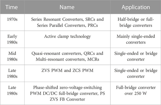
TABLE 1. Development history of soft-switching technology.
In the early 1970s, soft-switching technology mainly used series or parallel resonance technology. The DC converter is also called a resonant converter. The resonant converter has three modes of operation defined by the switching frequency. f is the working frequency and fr is the resonant frequency. When f < 1/2fr, the resonator is in the current discontinuous working mode, and the switch tube works under the condition of ZCS. When 1/2fr < f < fr, the resonant tank is capacitive. Therefore, the current leads the voltage when the switch is turned off, and the overlap area becomes smaller. However, the current-voltage overlap area becomes more significant when the switch is turned on as hard-switching. When fr < f, the resonant circuit is inductive, and the switch tube is turned on with ZVS, but the hard-switching happens when turning off. Series or parallel resonance technology is used in some communication switching power supplies, and the switching frequency ranges from 180 to 450 kHz.
The active clamp ZVS technology proposed later is mainly used in single-ended converters (Wan and Liu, 2000). The references proposed an active clamp ZVS PWM converter design for satellite power supply. Such converters can be implemented with single-ended forward and fly back circuits and their combinations. Taking the active clamp single-ended fly back converter as an example, this converter adds a clamping capacitor and a MOSFET as a clamping switch on the basis of the PWM single-ended fly back circuit. The circuit also utilizes the resonance in the circuit. The parasitic capacitor of the MOSFET and the inductor in the transformer or coupling inductor resonate, so that the main switch can be turned on at zero voltage.
Based on S-P resonance technology, quasi-resonant conversion technology and multi-resonance conversion technology became popular in the next decade. Initially, it is to realize the soft-switching of the converter composed of a single tube. Still, the push-pull converter, the half-bridge converter, and the full-bridge converter can also participate in the quasi-resonant converter and the multi-resonant converter. The difference between the quasi-resonant converter and the series-parallel resonance technology proposed in the 1970s is that it adds a resonant inductor and a resonant capacitor to the DC converter in the resonant converter. This resonant inductor and resonant capacitor re-constitute a resonant tank. According to the different combinations of series and parallel of inductor and capacitor in the resonant tank, the switch tube can realize ZVS or ZCS (Lee, 1988). The resonant tank of a multi-resonant converter is different from that of a quasi-resonant converter. The resonant tank of the multi-resonant converter is composed of the general resonant tank, the leakage inductor of the transformer and the parasitic capacitor in the circuit (Tabisz and Lee, 1989). According to the working principle of multi-resonant converter and quasi-resonant converter, it can be seen that they also use frequency modulation. This is also a disadvantage because it is challenging to design the output filter for the system using frequency modulation. Therefore, quasi-resonant converters and multi-resonant converters are generally used in low power, low voltage and strict requirements on volume and weight.
Since the early resonant circuits all required frequency modulation control, which brought great difficulty to the design of the filter, the converter based on constant frequency control was proposed in the later period. This kind of converter is also called the ZVS PWM converter. The ZVS PWM converter adds an auxiliary switch tube to the quasi-resonant converter in the circuit structure. It controls the resonant tank by controlling the conduction of the auxiliary switch tube. In the ZVS PWM converter, the resonant tank does not always participate in the resonance as previous but only works in resonance at the moment when the switch tube is switching (Ruan, 2003). Therefore, the working time of the resonant tank occupies only a small part of the switching period.
Full-bridge converters are generally used in medium and high-power occasions such as electric vehicle charging. Especially the Primary-side Phase Shifted (PPS) Full-Bridge (FB) DC-DC converter is widely used (Narimani and Moschopoulos, 2013; Yadav and Narasamma, 2014; Safaee et al., 2015; Chen et al., 2015; Chen et al., 2014; Sun et al., 2014). It adopts the phase-shift control method, uses the circuit’s own parameters to resonate to achieve soft-switching, and maintains the PWM technology’s characteristics of adjustable duty cycle based on constant frequency (Li et al., 2017). This method was used in this study. More importantly, the changing trends of auxiliary circuits for static charging and dynamic charging of electric vehicles are presented. In this way, in different charging environments of electric vehicles, the circuit can be operated in a high-efficiency environment by switching the auxiliary circuit. The specific details and experiments are presented in the following.
2 Analysis and control of wireless power transmission systems
The main circuit of the wireless charging system used in this paper is shown in Figure 2. The full-bridge inverter consists of a DC source and four MOSFETs which are Q1 to Q4. D1 to D4 is the intrinsic diodes of Q1 to Q4 and C1 to C4 is the corresponding capacitor. The resonant tank circuit adopts S-S compensation circuit. Lp and Ls are represented the inductors on the primary and secondary side coils, respectively and M is the mutual inductor. Cp and Cs are the compensated capacitor. Meanwhile ip and is denotes the currents of primary and secondary circuit, respectively. DR1 to DR4 represent the four diodes in full-bridge rectifier. Cf is the filter capacitor and RLd is the load resistor in secondary circuit.
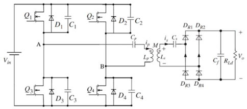
FIGURE 2. Topology of two-stage WPT system.
The wireless charging system uses the phase-shifted full-bridge control mode. Q1 and Q3 are called leading legs, and Q2 and Q4 are called lagging legs. Figure 3 shows a possible switching signal waveform for MOSFETs.
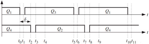
FIGURE 3. Example signal waveform of MOSFETs.
A stable output voltage is essential for wireless charging systems. The control loop can generates two sine waves with the phase difference and converts the sine waves into square waves with the same frequency through the comparator. These square waves are the input conduction signals for MOSFETs. Thus, a wireless charging system loop with controllable output voltage is obtained.
However, when the system is at the light load condition, the switching tube will have apparent conduction loss due to the large phase shift, which is called hard switching. The following article will analyze in detail the process of hard-switching in the WPT system. The different switching modes for the WPT system is shown in Figure 4.
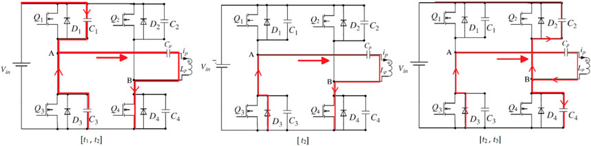
FIGURE 4. Equivalent circuits of different switching modes in hard-switching condition.
Some assumptions are made before the analysis: 1) All switching devices are ideal; 2) All capacitors and inductors are ideal regardless of their internal resistor; 3) The intrinsic capacitors of the four MOSFETs are all equal in value.
At t1, Q1 is turned off. The primary current ip begins to charge C1 and discharge C3. When the voltage of C1 increases to Vin and the voltage of C3 decreases to 0, which makes D3 conduct at t1. Then D3 clamping the voltage of C3 at 0. Therefore, Q3 can achieve ZVS. At t2, Q4 is turned off. The primary current ip still does not reach 0, charging C4 and discharging C2. However, when the system is at light load condition, ip is already very small. Therefore, although ip can charge and discharge Q2 and Q4, it cannot complete the charge and discharge process. As a result, Q2 and Q4 cannot achieve ZVS. At t3, Q2 is turned on. ip flows from B to A in reverse.
According to the above analysis, it can be concluded that under the light load condition, the phase shift of the feedback system output is very large. Hence the lagging leg cannot achieve ZVS and result a significant loss while the leading leg will not have such hard-switching problem. Therefore, although the system can realize the controllable output voltage, it needs to solve the conduction loss problem of the lagging leg.
3 Solutions and analysis to improve hard-switching in WPT systems
In Chapter 2, ip drops to 0 before charging and discharging the lagging leg is done. If ip is large enough to finish the charging and discharging, Q2 can achieve ZVS. Hence it is considered to place a current source at point B, as shown in Figure 5A. The current source is to increase the charging current for the lagging leg to complete the charging and discharging process, and it is typically modelled with a large inductor. The circuit topology after replacing the current source with an inductor is shown in Figure 5B and La is the auxiliary inductor.
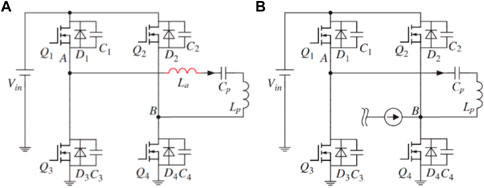
FIGURE 5. Proposed soft-switching circuit. (A) is the topology after adding the current source; (B) is the topology after replacing the current source with an inductor.
The control circuit in the WPT system has not changed. The control circuit still feeds back the load voltage mentioned in Chapter 2 and controls the output voltage by adjusting the phase shift. The auxiliary inductor in the full-bridge inverter is only to solve the hard-switching problem. The following article will analyze the working process of the improved circuit. After adding the auxiliary inductor, the signal for the MOSFETs and the waveform of current and voltage between points A and B are shown in Figure 6.
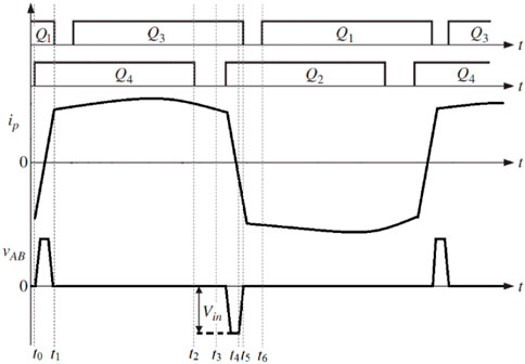
FIGURE 6. Waveforms of MOSFETs control signals, VAB, and ip for the proposed soft-switching circuit.
In order to better analyze this circuit, the following assumptions are made: 1)All switching devices are ideal; 2)All capacitors and inductors are ideal regardless of their internal resistor; 3)The intrinsic capacitors of the MOSFETs are all equal in value.
The current flow diagram at different time periods is shown in the Figure 7.
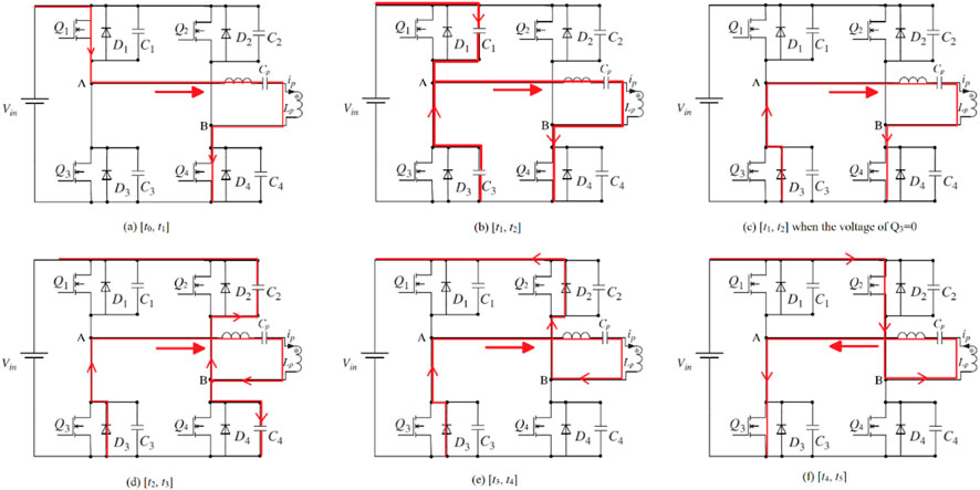
FIGURE 7. Equivalent circuits of different switching modes in soft-switching condition.
1. Mode 0 (t0, t1) (Figure 7A):
2. Mode 1 (t1, t2) (Figures 7B, C):
Both Q1 and Q4 are on. UAB = Vin. The primary current ip goes from point A to point B.
3. Mode 2 (t2, t3) (Figure 7D):
At t1, Q1 is turned off. The primary current ip begins to charge C1 and discharge C3, as shown in Figure 7B. The voltage of the two capacitors will gradually change. When the voltage of C1 increases to Vin and the voltage of C3 decreases to 0, which makes D3 conduct, clamping the voltage of C3 at 0, as shown in Figure 7C. Therefore, if Q3 turn on after that time, it can achieve ZVS.
At t2, Q4 is turned off. The primary current ip charges C4 and discharges C2. Since the primary side of the circuit is now inductive, the time for the current to drop to 0 can be greatly increased, providing additional time for the charging and discharging process. As a result, C2 can successfully end the discharge process until D2 turns on and clamps the voltage of Q2 to 0. This provides a prerequisite for Q2 to realize ZVS conduction.
4. Mode 3 (t3, t4) (Figure 7E):
The charging and discharging process is completed at t3. If Q2 turns on after t3, it can achieve ZVS. After t3, Q2 and Q3 have already turned on. UAB = −Vin. ip goes down linearly to 0 and then begins to increase reversely.
5. Mode 4 (t4, t5) (Figure 7F):
ip still increases during this period. At t6, Q3 is turned off and the circuit operate like Mode 1, which is the beginning of the second switching period. The second half-switching period is similar to the first half period.
As can be seen from Figure 7, the auxiliary inductor can solve the hard-switching problem of the lagging leg. After adding the auxiliary inductor, the current and voltage overlapping area disappear, resulting in almost no conduction loss. Hence, the efficiency is improved compared to the previous one. Moreover, the added inductor does not affect the work of the control loop, so the improved WPT system can realize soft-switching conduction while controlling the output voltage.
In order to simplify the circuit and reduce the EMI brought by the auxiliary inductor, it can be considered making the primary side circuit inductive without auxiliary inductor. Since the operating frequency of the resonant tank is inconvenient to adjust, the resonant capacitor on the primary side can be changed. Increasing the capacitor value can make the primary side circuit inductive rather than resistive at the original resonant frequency. The resonator on the secondary side still works as fully compensated mode at the initial operating frequency, so it remains resistive. This improvement method just replaces the auxiliary inductor by adjusting the circuit parameters to make the circuit inductive. It will not affect the control circuit.
4 Simulation results
Three simulations were performed as follows:
1. First, the experiment observes whether the control circuit can stabilize the system output voltage at the reference value. At the same time, the current and voltage waveform of lagging leg in the circuit is observed to determine whether ZVS can be achieved.
2. Then, according to the increase of the auxiliary inductor, the switch tubes can all work in the conduction state of the soft switch so that the loss of the circuit can be significantly reduced.
3. Finally, when the power supply voltage fluctuates, and the load resistor fluctuates, the system can still output an ideal voltage to ensure the soft-switching working state.
The parameter values of the switch tube are unchanged in the three simulations and they are shown in the Table 2.
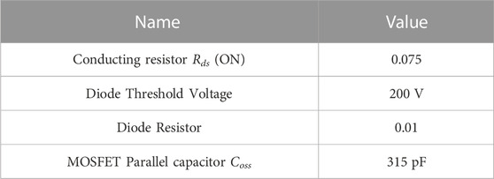
TABLE 2. MOSFET ratings.
4.1 Simulation of WPT systems without auxiliary circuits
The circuit does not contain the auxiliary inductor and the resonator operates at the resonant frequency. The full-bridge inverter works in the phase-shift mode, and the four switches are controlled by the PS modulation. Table 3 shows the values of various parameters in the circuit. Kp and KI are the parameters of the PI controller. Kp represents the proportional control coefficient, and KI represents the integral control coefficient.
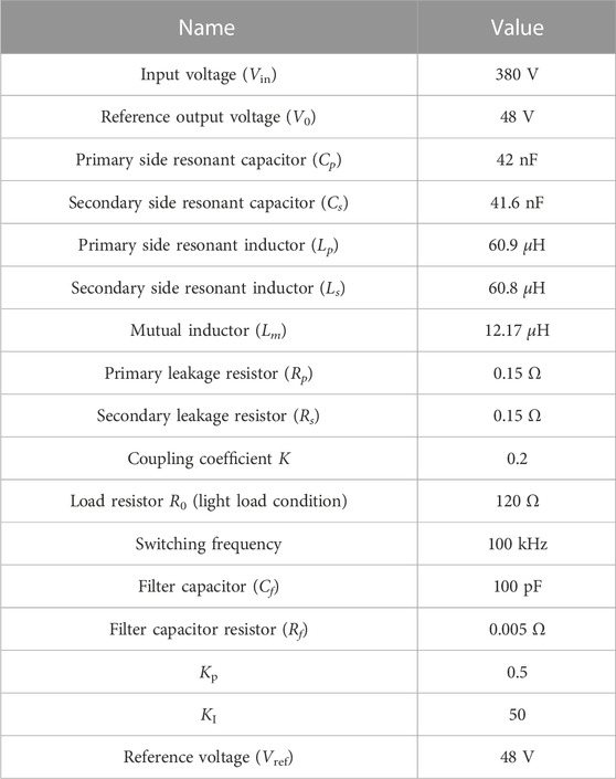
TABLE 3. Key ratings in main circuit.
Under light load conditions, the phase of the control circuit output will reach more than 160°. As shown in Figure 8, the output phase reaches 178.6°. When the circuit reaches a stable state, the output voltage is consistent at 48.13 V which is very similar to the reference voltage.
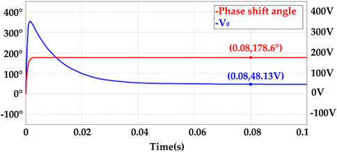
FIGURE 8. The waveform of output voltage and the phase shift angle in WPT system without optimization.
The voltage and current waveforms when the leading leg Q1 is turned on and off are shown in the Figure 9A. It can be seen that when Q1 is turned on, there is no overlap area between voltage and current, indicating that Q1 can realize ZVS conduction and Q1 has no conduction loss. The voltage and current waveform of Q3 is exactly the same as that of Q1, so there is no hard-switching problem in the leading leg in the WPT system. The upper part of Figure 9A is an overview of the waveforms, and the lower part shows the details of the voltage and current waveforms when Q1 conducts. Figure 9B shows the voltage and current relationship of Q2 during operation. It can be seen that when Q2 is turned on, the current increases while the voltage decreases and the two have an overlapping area. The part covered by the dotted line in the black circle in Figure 9B is the conduction loss generated by Q2. Q4 works the same as Q2. The lagging leg cannot achieve soft-switching when turning on, resulting in conduction loss. These losses reduce the overall efficiency of the circuit.
FIGURE 9. Current waveform and voltage waveform. (A) is waveform of Q1 in WPT system without optimization; (B) is waveform of Q2 in WPT system without optimization.
According to the simulation results, it can be concluded that the control circuit in the WPT system can make the circuit output an ideal voltage. But in the full-bridge converter, there is conduction loss in the lagging leg, so the efficiency of the circuit will be decreased.
4.2 Simulation of WPT systems with auxiliary circuits
According to the theory in Chapter 3, an inductor is added to the resonant tank in this simulation. The inductor is 20
Figure 10 shows the output voltage when the system is stable and the phase difference. The simulation time is set to 0.15 s. It can be seen that the system output voltage can quickly reach 48.2 V within 0.15 s. When the system reaches the steady state, the phase difference between the leading leg and the lagging leg is different. But both can output the ideal voltage in time so that the control circuit can work well in the improved system.
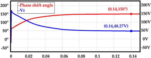
FIGURE 10. The waveform of output voltage and the phase shift angle in the optimized circuit.
Figure 11A shows the current-voltage waveforms of Q1 at turning on stage. Q1 can still achieve soft-switching. The voltage and current waveforms of Q3 are the same as those of Q1. The added auxiliary inductor does not affect the working state of the leading leg. Figure 11B shows the current and voltage waveforms when Q2 is turned on. In the black circle, the current and voltage have no overlapping area. The current of Q2 shows the same trend as Q1. It increases in the negative direction and then rises again. It is because that the discharge current does not decrease to 0 before Q2 turns on. The current direction is opposite to Q2’s voltage direction, which means that Q2 has completed the discharge process before turning on. Therefore, ZVS can be turned on. The conduction process of Q4 is the same as that of Q2. The lagging leg can achieve ZVS conduction with the help of the auxiliary inductor.
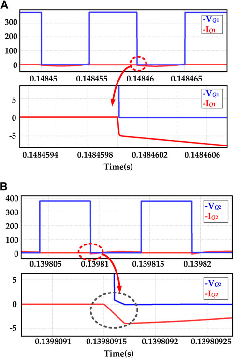
FIGURE 11. Current waveform and voltage waveform. (A) is the waveform of Q1 in the optimized circuit; (B) is the waveform of Q2 in the optimized circuit.
It can be seen from the experimental results of the second experiment that after adding the auxiliary inductor, the voltage of the system is still controllable. At the same time, the lagging leg’s hard-switching problem is solved, the conduction loss of the circuit is greatly reduced, and the overall efficiency is improved.
4.3 Simulation of WPT system with auxiliary inductor in special cases
In order to verify the stability of the system, the input of the DC power supply is fluctuated by 10% and the load resistor will be adjusted at another moment. In the simulation, the load resistor is set to abruptly changed at 0.1 s. The power supply voltage is set to have the maximum voltage fluctuation at 0.2 s in this simulation. The circuit parameters of the circuit are completely consistent with the former simulation, and the parameters of the control circuit also remain unchanged.
According to Figure 12, at 0.1 s, the load suddenly changed from 120 to 20 at 0.1 s. The power supply voltage changed from 380 to 418 V at 0.2 s. The two area inside the black circle are the fluctuation of output voltage, but the output voltage recovered to the reference voltage of 48 V quickly. At the moment of 0.2 s, the power supply voltage fluctuated to the greatest extent, and the output voltage was immediately affected, resulting in a slight fluctuation. But the voltage also recovered to 48.2 V within 0.5 s and then slowly returned to the exact 48 V.
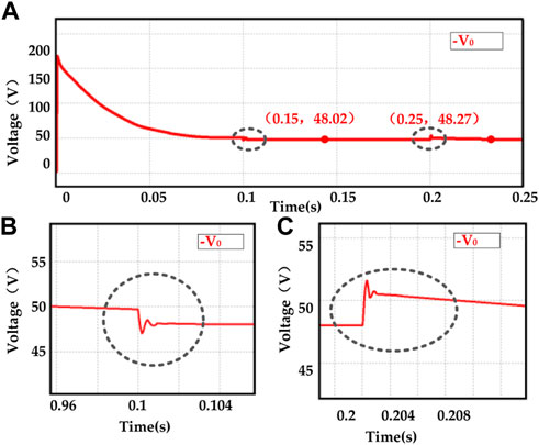
FIGURE 12. The waveform of output voltage. (A) is the overview waveform; (B) is the detail waveform when the resistor changes; (C) is the detail waveform when the input voltage changes.
Figure 13A shows the waveform of the voltage and current of the lagging leg when load changes. Figure 13B shows the waveform of the lagging leg when input voltage changes. Both of the two waveforms are obtained when the system become stable again. After changes, the voltage can always return to the referenced value and there were still no hard-switching issues in the circuit.
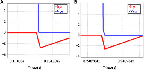
FIGURE 13. (A,B) are the waveform diagram of the current and voltage of Q2 when the output voltage is stable, respectively.
5 Experimental verification
5.1 Experimental setup
In order to verify whether the auxiliary inductor can achieve ZVS, experiments were conducted without auxiliary inductor first. Then an auxiliary inductor was added at the primary side circuit for comparison. Both experiments should satisfy the output voltage is controllable. The current and voltage waveforms of output on the full-bridge inverter side and input on the full-bridge rectifier side are observed with an oscilloscope. The full-bridge inverter adopts the phase-shift control mode. The topology of the experimental setup is shown in Figure 14. As shown in Figure 14, The circuit consists of a DC source, a full-bridge inverter, a resonator, a full-bridge rectifier and a load.
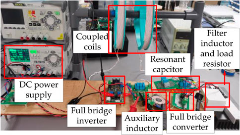
FIGURE 14. Photograph of the experimental setup.
A scale-down setup is used in the experiment. The experimental parameters are shown in the Table 4.
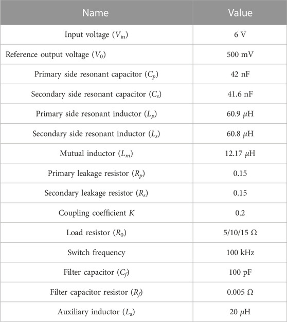
TABLE 4. Ratings in experimental circuit.
5.2 Experiment results
5.2.1 Experiment of MOSFETs to realize soft-switching
Figure 15A shows the system input and output voltage and current waveforms when the load is 10 and 15 without auxiliary circuits. uAB and iAB is the current and voltage of the input side of the resonator. used and ised is the current and voltage of the output side of the resonator.
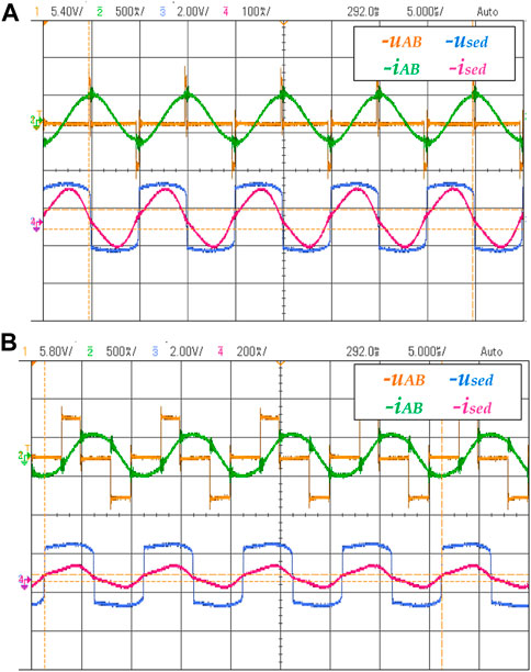
FIGURE 15. (A,B) are the waveform of the current and voltage on the primary and secondary sides of the resonator without and with the auxiliary inductor, respectively.
It can be seen from the waveform of the voltage and the current that the primary side of the circuit is resistive because the resonator was working in a fully compensated state. When the output voltage reaches the reference value of 500 mV, the phase difference is 171°. It can be speculated that the switch tube cannot achieve ZVS. The voltage waveform of the output terminal of the resonator is similar to a rectangular wave. Unlike the voltage waveform of the input side, the waveforms on the output side do not have a large dead zone. The current waveform resembles a sinusoidal waveform.
Figure 15B shows the waveform after adding the auxiliary inductor.
Figure 16 shows that the primary-side output voltage waveform leads the current waveform significantly, indicating that the primary-side loop is inductive. Crucially, it can be seen that when the primary side voltage is reversed, the current has not yet crossed 0 and changed. According to the theory in Chapter 3, due to the charging and discharging process of the lagging leg, the primary side current will not reverse immediately after the voltage becomes reversed, as shown in the Figure 7E. It will linearly decrease to 0 and then reverse. Therefore, it can be concluded that the switch tube of the circuit works in a soft-switching state at this time. The conduction losses of the circuit are significantly reduced.
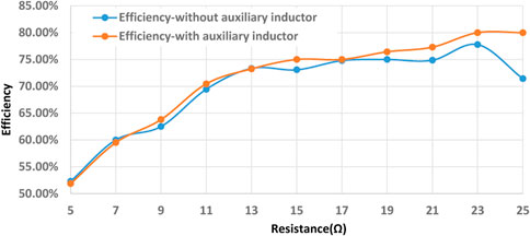
FIGURE 16. The comparison of the inverter efficiency by adding the auxiliary inductor and without using the auxiliary inductor.
According to the experimental data measured in the experiments, it can be seen that the efficiency of the circuit is improved after using the auxiliary inductor. Figure 16 is a graph derived from all the data. Adding auxiliary circuits can improve the working efficiency of the converter under the majority of load conditions. Especially when the load is large, the circuit efficiency improvement is more prominent.
5.2.2 Experiment to achieve ZVS with the maximum power factor (PF) of the circuit
The experiment aims to test the optimal resistor value range of the load when adding different auxiliary inductors. Adding an extra series inductor or decreasing the value of the capacitor on the transmitter side resonator can make the system inductive to help the MOSFETs to achieve soft switching. However, when the auxiliary circuit makes the primary circuit more inductive, it also causes more reactive power and reduces the overall efficiency of the circuit. Therefore, it is necessary to discuss the load range corresponding to different degrees of inductive auxiliary circuits so that the circuit can work at high efficiency. When the MOSFETs in the primary side circuit can realize ZVS, and PF of the circuit is also the largest, the reactive power in the circuit is the least.
During the charging process of an electric vehicle, the resistor of the battery changes over time. Furthermore, when the electric vehicle still moves, the distance between the primary side coil and the secondary side coil is constantly changing, which causes the mutual inductor fluctuations. Therefore, the experiment is carried on to figure out the relationship between the load resistor and mutual inductor range corresponding to different auxiliary circuits. In the experiment, the primary side circuit is inductive by increasing the capacitor of the resonator. In this way, it is only necessary to connect a capacitor parallel with the original circuit to achieve adjustment.
The voltage and current waveforms on the primary side displayed by the oscilloscope are used as a reference to determine whether the MOSFET is at the critical point of hard switching and soft switching. If the current is positive when the voltage jumps from 0 to a positive value, the primary side’s MOSFETs work at hard switching, referring to the theory in Chapter 2. The waveform relationship between voltage and current is shown in Figure 17A. uAB and iAB is the voltage and current waveform of primary side; used and ised is the voltage and current waveform of secondary side. If the current is negative when the voltage jumps from 0 to a positive value, the MOSFETs on the primary side are soft-switching, and the circuit on the primary side generates redundant reactive power. The relationship between the voltage and current waveforms is shown in Figure 17B. When the voltage suddenly changes and the current is 0 simultaneously, the auxiliary circuit makes the MOSFETs achieve soft-switching while the PF of the circuit is the least. The waveform relationship between voltage and current at this time is shown in the Figure 17C.
FIGURE 17. (A) is waveforms of the current and voltage on the primary and secondary sides when the MOSFETs work in hard-switching state; (B) is waveforms of the current and voltage on the primary and secondary sides when the MOSFETs work in soft-switching state with redundant reactive power; (C) is waveforms of the current and voltage on the primary and secondary sides when the auxiliary circuit can just make the MOSFETs achieve soft switching.
First, the distance of the coil is set to 2.6 cm, and the capacitor value of the auxiliary circuit is adjusted at 5, 9, 11, 13, and 14 nF, respectively. Other parameters of the experiment are shown in the Table 5. After each capacitor is connected in parallel, the load resistor value is adjusted continuously to find when the circuit satisfies soft-switching through the oscilloscope. The resistor value will be recorded when the MOSFETs can achieve soft-switching with minor reactive power. From the measured data, Figure 18 can be obtained. Under the condition that the distance between the coils remains the same, increasing the capacitor value of the auxiliary circuit will increase the upper limit of the circuit load resistor. The recorded resistor value is the maximum load that satisfies the soft-switching condition.
TABLE 5. Parameters in experimental circuit.
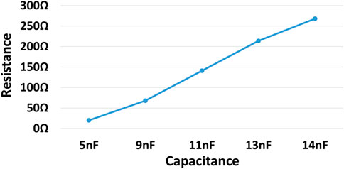
FIGURE 18. The curve of the maximum value of the load resistor, after five groups of auxiliary capacitors are connected in parallel.
The relationship between the coil distances corresponding to different capacitor values will be tested while the load resistor remains unchanged. The load resistor is set to be 40 Ω. The different capacitor values are the same as in the previous experiment. The experiment tested the coil distance to make the MOSFETs achieve soft switching with minor reactive power. Figure 19 is obtained according to the measured data. The left and right values of the table represent the mutual inductor values between the coils at various distances. It can be seen that when the coil distance becomes smaller, a larger capacitor needs to be provided to enable the primary side switch tube to achieve soft switching.
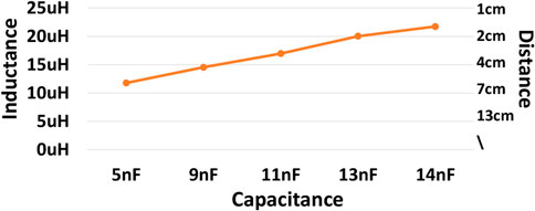
FIGURE 19. The curve of the distance of the coupled coil, after five groups of auxiliary capacitors are connected in parallel.
During static charging, considering that the resistor of the battery will continue to increase, it is necessary to increase the inductor or capacitor of the auxiliary circuit to maintain the soft-switching state of the circuit. During dynamic charging, the mutual inductor will change will the coil misalignment. Electric vehicles can switch capacitors in different gears according to the changing trend of auxiliary capacitors tested in the paper to make the circuit achieve ZVS.
6 Conclusion
This paper proposes an auxiliary method to help the switches in the full-bridge inverter achieve soft-switching in WPT systems. By adding an auxiliary inductor on the primary side of the resonator, the MOSFETs can easily achieve ZVS, thereby reducing the conduction loss. Both simulation and experiments confirm that the increased auxiliary inductor can improve the efficiency of the circuit according to less conduction loss without affecting the operation of the control circuit. Meanwhile, the simulation verifies that the control circuit can still work with the auxiliary inductor even when the power grid fluctuates or the load changes. Finally, the paper simulates the requirements for auxiliary circuits when charging electric vehicles in different scenarios through experiments.
Data availability statement
The original contributions presented in the study are included in the article/supplementary material, further inquiries can be directed to the corresponding author.
Author contributions
CL is responsible for the writing of the methodology, simulation verification, and experiments in the paper. The supervision, review and editing of the papers are mainly carried out by KW and YM. All authors have read and agreed to the published version of the manuscript.
Funding
This research was funded by the Guangdong Basic and Applied Basic Research Foundation 2022A1515010708 and Innovation and Technology Fund ITP/047/21AP.
Conflict of interest
The authors declare that the research was conducted in the absence of any commercial or financial relationships that could be construed as a potential conflict of interest.
Publisher’s note
All claims expressed in this article are solely those of the authors and do not necessarily represent those of their affiliated organizations, or those of the publisher, the editors and the reviewers. Any product that may be evaluated in this article, or claim that may be made by its manufacturer, is not guaranteed or endorsed by the publisher.
References
Chen, Z., Liu, S., and Wang, Y. (2014). A new ZVS full-bridge converter with active-regulating auxiliary current. Trans. China Electrotech. Soc. 29 (4), 1–9. doi:10.1109/ECCE.2012.6342443
Chen, Z., Wang, Y., and Li, M. N. (2015). Wide range zero voltage switching phase-shifted full-bridge converter with low circulation loss. Trans. China Electrotech. Soc. 30 (22), 71–79. doi:10.1109/TPEL.2012.2227280
Covic, G. A., and Boys, J. T. (2013). Inductive power transfer. Proc. IEEE 101 (6), 1276–1289. doi:10.1109/JPROC.2013.2244536
Deng, J. J. (2015). Research on high-efficiency resonant converter of on-board charger for electric vehicle. Degree of Doctor of Philosophy. Xi’an China: Northwestern Polytechnical University.
Deng, J., Mao, Y., and Yang, Y. (2020). Distribution power loss reduction of standalone DC microgrids using adaptive differential evolution-based control for distributed battery systems. Energies 13, 2129. doi:10.3390/en13092129
Dragičević, T., Lu, X., Vasquez, J. C., and Guerrero, J. M. (2016). DC microgrids—Part II: A review of power architectures, applications, and standardization issues. IEEE Trans. Power Electron. 31 (5), 3528–3549. doi:10.1109/TPEL.2015.2464277
Lee, F. C. (1988). High-frequency quasi-resonant converter technologies. Proc. IEEE 76 (4), 377–390. doi:10.1109/5.4424
Li, H. M., Zhang, H. G., and Cui, C. (2017). A review of research on PWM soft-switching DC-DC converters for on-board charging. CES Trans. Electr. Mach. Syst. (CES TEMS) 32 (24), 59–70. doi:10.19595/j.cnki.1000-6753.tces.160709
Li, S. Y. (2015). Design of 75kW phase-shifted full-bridge ZVS DC/DC converter. Master Degree. Harbin China: Harbin Institute of Technology.
Narimani, M., and Moschopoulos, G. (2013). A new DC/DC converter with wide-range ZVS and reduced circulating current. IEEE Trans. Power Electron. 28 (3), 1265–1273. doi:10.1109/TPEL.2012.2207404
Qian, X., Yang, Y., Li, C., and Tan, S. C. (2020). Operating cost reduction of DC microgrids under real-time pricing using adaptive differential evolution algorithm. IEEE Access 8, 169247–169258. doi:10.1109/ACCESS.2020.3024112
Rim, C. T., and Chris, M. (2017). Wireless power transfer for electric vehicles and mobile devices. New York: Wiley.
Roslan, M. A., Nanda, N. N., and Yusoff, S. H. (2021). Series-series and series-parallel compensation topologies for dynamic wireless charging. IIUM Eng. J. 22 (2), 199–209. doi:10.31436/iiumej.v22i2.1660
Ruan, X. B. (2003). Soft-switching technology of DC switching power supply. 2nd ed. Beijing, China: Science Press, 118–134.
Safaee, A., Jain, P. K., and Bakhshai, A. (2015). An adaptive ZVS full-bridge DC-DC converter with reduced conduction losses and frequency variation range. IEEE Trans. Power Electron. 30 (8), 4107–4118. doi:10.1109/TPEL.2014.2357815
Sun, T. C., Guo, C., and Naren, T. (2014). A novel DC-DC ZVS full-bridge converter based on phase shift control. Trans. China Electrotech. Soc. 29 (12), 66–72. doi:10.1109/IAS.2004.1348713
Tabisz, W. A., and Lee, F. C. (1989). “DC analysis and design of zero-voltage-switched multi-resonant converters,” in 20th Annual IEEE Power Electronics Specialists Conference, 243–251.
Tang, X. C. (2012). Research on LLC resonant converter based on digital control. Degree of Master of Engineering. Nanjing China, March: Nanjing University.
Wan, C. A., and Liu, W. G. (2000). Active clamp ZVS-PWM switching converter application. Aerosp. Technol. 01, 21–25.
Yadav, G. N. B., and Narasamma, N. L. (2014). An active soft switched phase-shifted full-bridge DC-DC converter: Analysis, modeling, design, and implementation. IEEE Trans. Power Electron. 29 (9), 4538–4550. doi:10.1109/TPEL.2013.2284780
Yang, Y. (2020). “Development of front-end monitoring of mutual coupling and load conditions in wireless power transfer systems,” in 8th International Conference on Power Electronics Systems and Applications (PESA), 1–5.
Yang, Y., Qin, Y., Tan, S. C., and Hui, S. Y. R. (2019a). Efficient improvement of photovoltaic-battery systems in standalone DC microgrids using a local hierarchical control for the battery system. IEEE Trans. Power Electron. 34 (11), 10796–10807, Nov. doi:10.1109/TPEL.2019.2900147
Yang, Y., Tan, S. C., and Hui, S. Y. R. (2019b). “Communication-free control scheme for Qi-compliant wireless power transfer systems,” in IEEE Energy Conversion Congress and Exposition (ECCE), 4955–4960. doi:10.1109/ECCE.2019.8912496
Yang, Y., Tan, S. C., and Hui, S. Y. R. (2018). Mitigating distribution power loss of DC microgrids with DC electric springs. IEEE Trans. Smart Grid 9 (6), 5897–5906, Nov. doi:10.1109/TSG.2017.2698578
Yang, Y., Tan, S. C., and Hui, S. Y. R. (2021). “State-of-charge balance control of distributed battery systems with distinct state-of-health in DC microgrids,” in IEEE/IAS Industrial and Commercial Power System Asia (I&CPS Asia), 140–144. doi:10.1109/ICPSAsia52756.2021.9621493
Keywords: wireless power transfer (WPT), DC microgrids, optimal efficiency, zero voltage switching (ZVS), output voltage regulation
Citation: Li C, Wang K and Mao Y (2023) Design of a wireless charging system in DC microgrids with accurate output regulation and optimal efficiency. Front. Electron. 4:968549. doi: 10.3389/felec.2023.968549
Received: 14 June 2022; Accepted: 27 February 2023;
Published: 17 March 2023.
Edited by:
Zhengmao Li, Nanyang Technological University, SingaporeReviewed by:
Wenzheng Xu, Beijing Jiaotong University, ChinaAshokkumar Srinivasan, Jawaharlal Nehru Technological University, Hyderabad, India
Copyright © 2023 Li, Wang and Mao. This is an open-access article distributed under the terms of the Creative Commons Attribution License (CC BY). The use, distribution or reproduction in other forums is permitted, provided the original author(s) and the copyright owner(s) are credited and that the original publication in this journal is cited, in accordance with accepted academic practice. No use, distribution or reproduction is permitted which does not comply with these terms.
*Correspondence: Yuan Mao, bWFveXVhbkB6anV0LmVkdS5jbg==